EP0558855A2 - Leiterplattenstapel mit neuen cross-over-Zellen - Google Patents
Leiterplattenstapel mit neuen cross-over-Zellen Download PDFInfo
- Publication number
- EP0558855A2 EP0558855A2 EP92311248A EP92311248A EP0558855A2 EP 0558855 A2 EP0558855 A2 EP 0558855A2 EP 92311248 A EP92311248 A EP 92311248A EP 92311248 A EP92311248 A EP 92311248A EP 0558855 A2 EP0558855 A2 EP 0558855A2
- Authority
- EP
- European Patent Office
- Prior art keywords
- cross
- accordance
- slug
- frame
- substrates
- Prior art date
- Legal status (The legal status is an assumption and is not a legal conclusion. Google has not performed a legal analysis and makes no representation as to the accuracy of the status listed.)
- Withdrawn
Links
Images

Classifications
-
- H—ELECTRICITY
- H01—ELECTRIC ELEMENTS
- H01R—ELECTRICALLY-CONDUCTIVE CONNECTIONS; STRUCTURAL ASSOCIATIONS OF A PLURALITY OF MUTUALLY-INSULATED ELECTRICAL CONNECTING ELEMENTS; COUPLING DEVICES; CURRENT COLLECTORS
- H01R12/00—Structural associations of a plurality of mutually-insulated electrical connecting elements, specially adapted for printed circuits, e.g. printed circuit boards [PCB], flat or ribbon cables, or like generally planar structures, e.g. terminal strips, terminal blocks; Coupling devices specially adapted for printed circuits, flat or ribbon cables, or like generally planar structures; Terminals specially adapted for contact with, or insertion into, printed circuits, flat or ribbon cables, or like generally planar structures
- H01R12/70—Coupling devices
- H01R12/71—Coupling devices for rigid printing circuits or like structures
- H01R12/712—Coupling devices for rigid printing circuits or like structures co-operating with the surface of the printed circuit or with a coupling device exclusively provided on the surface of the printed circuit
- H01R12/714—Coupling devices for rigid printing circuits or like structures co-operating with the surface of the printed circuit or with a coupling device exclusively provided on the surface of the printed circuit with contacts abutting directly the printed circuit; Button contacts therefore provided on the printed circuit
-
- H—ELECTRICITY
- H01—ELECTRIC ELEMENTS
- H01R—ELECTRICALLY-CONDUCTIVE CONNECTIONS; STRUCTURAL ASSOCIATIONS OF A PLURALITY OF MUTUALLY-INSULATED ELECTRICAL CONNECTING ELEMENTS; COUPLING DEVICES; CURRENT COLLECTORS
- H01R13/00—Details of coupling devices of the kinds covered by groups H01R12/70 or H01R24/00 - H01R33/00
- H01R13/02—Contact members
- H01R13/22—Contacts for co-operating by abutting
- H01R13/24—Contacts for co-operating by abutting resilient; resiliently-mounted
- H01R13/2407—Contacts for co-operating by abutting resilient; resiliently-mounted characterized by the resilient means
- H01R13/2414—Contacts for co-operating by abutting resilient; resiliently-mounted characterized by the resilient means conductive elastomers
Definitions
- This invention relates to cross-over connections between circuit boards and particularly to effecting very short, high-density electrical connections in assemblies of such boards without having to use the front or exposed surfaces of the boards.
- Circuit boards embodying complex computer architectures frequently are stacked or paired. Such boards typically mount "chips" which may, for example, be processors or memory stores. Frequently, several chips are mounted in a planar gang on a miltichip module. As the computing and storage capacities of these equipments grow to meet new demands of speed and computing power, there is a need to package the chip boards more effectively and to realize more effective communications paths between adjacent boards.
- the prior art cross-over cables also require substantial wiring lengths of, for example, three inches or more which significantly limits the speeds at which the computer may operate.
- An even further problem of the prior art design relates to crosstalk between crossover paths.
- one object of the invention is to provide a more reliable interconnection between adjacent chip-mounting circuit boards.
- Another object of the invention is to improve the speed of operation of stacked arrays of chip-containing circuit boards.
- a further object of the invention is to facilitate and simplify the assembly of such board arrays.
- a still further object of the invention is to make more reliable use of elastomeric one-directional conductive material to effect board-to-board connections.
- Another object of the invention is to realize a more dense packaging of computer components, particularly processors and memory chips.
- This invention is a highly efficient mechanism for achieving cross-over paths through a structural frame, using elastomeric one-dimensional conductive material.
- two chip-mounting substrates or boards are mounted on opposite sides of a structural frame.
- On the exterior side of each substrate are mounted one or more chips or discrete clusters of chips.
- One or more (usually several) discrete and separate areas on the interior side of each substrate are dedicated for the mounting of arrays of contact pads. These pads connect by various paths through and within the substrate to leads of the chips or chip arrays on the exterior side of the substrate.
- the frame includes interior passages through which either a gaseous or a liquid cooling fluid is conducted.
- the frame is provided with an array of cross-over cell cavities which for example may be substantially square in cross-section.
- Each cavity is aligned with a corresponding cross-over cell pad array on the adjacent substrate.
- Slugs of elastomeric one-directional conductive material are placed in each cavity.
- each cavity is nominally of substantially the same volume as an uncompressed slug.
- each slug may be formed with a somewhat lesser cross-sectional area than the cavity cross-section, but with a somewhat greater height than the thickness of the frame to provide an appropriate initial slug volume.
- Guide means are provided to align each substrate on respective sides of the frame so that the contact pad areas are facing each other and the intervening elastomer slug.
- Means also are provided for holding the two substrates together to compress the elastomeric material a predetermined amount while at the same time fastening the assembly. The elastomeric material thus compressed expands to fill and firmly lodge in its support chamber. The result is an assembly of two (or more) multi-chip module boards with internal cross-over cells which are sealed from contaminant and stabilized in their electrical conductivity by the close control over compressive forces and internal temperature made possible by the invention.
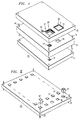
- the invention may be embodied in a assembly such as module assembly 10 which consists of two circuit card substrates 11 and 13 sandwiching a frame 12.
- An array of cross-over cell cavities 16 seen in FIG. 5 are formed through frame 12.
- the cavities 16 are shown uniformly arrayed, but may be placed in any convenient fashion.
- frame 12 with its cavities 16 is to form the cavities out of hollow open-ended square blocks, such as block 9 seen in FIG. 5, which fit into square openings provided in top and bottom plates of the frame 12 (plates not shown).
- the remainder of the interior space between the top and bottom plates may be provided with any desired shape to accommodate cooling fluid which, for example, may enter the assembly at coolant inlet 25 and exit at coolant outlet 26.
- the coolant may be gaseous, such as forced air or alternatively liquid such as ordinary brake fluid.
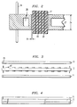
- slugs of elastomeric one-directional conductive material 17 are placed in the cavities 16. If the cavities are square in cross-section as in the instant embodiment, the slugs are substantially square in cross-section also. It is advantageous to shape the slugs so that each has a somewhat lesser cross-sectional area than that of the cavity as suggested by the dimension denoted 8 in FIG. 2. At the same time, the height of each slug 17 is made to be greater that the depth or top-to-bottom dimension of the cavity 16 denoted 24 in FIG. 2. In a preferred embodiment of the invention, the volume of the slugs 17, when compressed in the manner to be described, will approximate the volume of the cavity 16 and preferably will at least equal it.
- the substrates 11 and 13 include alignment holes 15 at each corner, which as seen also in FIGS. 3 and 4, mate with the four alignment pins 14 of frame 12. The alignment achieved is to assure that the cross-over cell pad arrays 18 appearing on the top surface of substrate 11 and the corresponding crossover cell pad arrays shown in dotted lines on the bottom of substrate 13 are in close vertical register.
- FIG. 1 shows an array of chip cavities 19 formed on the surface of substrate 13. Similar cavities (not shown) are formed in the substrate 11, the latter being symmetrically located with respect to the cavities 19 of substrate 11.
- the chip cavities 19 are a conventional way for containing in a frame such as frame 14, a multiplicity of semiconductor integrated circuits such as a multichip module 22.
- the cavities 19 have a conventional bonding ledge 16 inset within the cavity on all four sides of which bonding ledge pads 20 appear.
- Wire bond connections such as wire 7 in FIG. 1 are conventionally effected from the multichip module 7 to the pads 20.
- the pads 20, seen in FIG. 1, are connected by layered routing paths (not shown) within the interior of the substrates 11 and 13 in substantially any pattern or routing that is necessary to achieve the design of the computer architecture.
- the expedient of interior routing is well-known in the art; but while it does not form part of this invention, the invention greatly adds to the utility of the internal routing layers.
- connections from the pads 20 in each of the chip cavities 19 following internal routing eventually make appearances in cross-over cell pad arrays such as arrays 18 disposed on the interior surfaces of substrates 11 and 13.
- the slug 17 contains a series of vertical conductive paths denoted 23.
- Slugs of elastomeric material with vertical or one-directional paths that are usable in this invention may be formed by any of several methods of fabrication. For example, .010 mil thick elastomer sheets with closely spaced gold conductive paths silk-screened on one side thereof may be adherently stacked and slugs of the desired length and cross-section then cut from the stack.
- the cross-section of the vertically conductive paths 23 of the slugs 17 should be substantially less than the spacing between adjacent contact pads of the pad arrays 18 in order to prevent the shorting out of adjacent pads.
- the conductor-to-conductor spacing of the paths 23 should be appropriately dense to assure a maximum of electrically conductive paths between corresponding contact elements of the oppositely disposed cross-over cell pad arrays 18.
- the components of the assembly 10 are positioned as in FIG. 3 and then brought together by sliding the alignment holes 15 of the substrates 11 and 13 onto the alignment pins 14. In the assembled position, shown in FIG. 4, the slugs are compressed to substantially fill the cavities 16 with their compressed volume. For permanent sealing, the assembly may be bonded.
- FIG. 6 graphs roughly the behavior of one elastomeric vertically conductive material that may be used in the present invention.
- Elastomeric connectors may, for example, be realized by starting with an array of metal strips running linearly through a silicone rubber body typically .0005" thick and .002" wide arranged in rows approximately .004", which then are laminated together to form a bulk of directionally conductive material. Silicone formulations have the advantage of flexibility at temperatures below -65 degrees C, yet are tolerant of elevated temperatures up to +175 degrees C. Further, silicones are unaffected by aging and typically do not become sticky, brittle or cracked.
- Silicones show little or no degradation when exposed to ultra-violet radiation, oxygen, ozone or humidity.
- One suitable elastomeric material is available under the tradename "Matrix MOE” from Elastomeric Technologies, Inc. of Hatsboro, PA. Its behavior is depicted in FIG. 6. It is seen that as this material is compressed, its conductivity increases up to a point. An optimum range of maximum conductivity can be identified as a function of the pounds of applied compressive force in pounds per square inch occurring within a certain range. Thereafter, the conductivity decreases.
- FIG. 7 shows the invention being used in a conventional circuit board or card enclosure 29.
- the backplane 30 of the enclosure 29 contains the usual array of pin connectors 32.
- Rails 31 mount one or more (usually many) assemblies 10.
- the female gang connectors 33 which serve in conventional fashion as circuit paths to the outside world for each assembly 10 mate with pin connectors 32.
Landscapes
- Combinations Of Printed Boards (AREA)
- Multi-Conductor Connections (AREA)
- Coupling Device And Connection With Printed Circuit (AREA)
- Mounting Of Printed Circuit Boards And The Like (AREA)
Applications Claiming Priority (2)
| Application Number | Priority Date | Filing Date | Title |
|---|---|---|---|
| US84409992A | 1992-03-02 | 1992-03-02 | |
| US844099 | 1992-03-02 |
Publications (2)
| Publication Number | Publication Date |
|---|---|
| EP0558855A2 true EP0558855A2 (de) | 1993-09-08 |
| EP0558855A3 EP0558855A3 (en) | 1996-05-01 |
Family
ID=25291818
Family Applications (1)
| Application Number | Title | Priority Date | Filing Date |
|---|---|---|---|
| EP92311248A Withdrawn EP0558855A3 (en) | 1992-03-02 | 1992-12-10 | Circuit board stack with novel cross-over cells |
Country Status (2)
| Country | Link |
|---|---|
| EP (1) | EP0558855A3 (de) |
| JP (1) | JP2598212B2 (de) |
Cited By (13)
| Publication number | Priority date | Publication date | Assignee | Title |
|---|---|---|---|---|
| US5657206A (en) * | 1994-06-23 | 1997-08-12 | Cubic Memory, Inc. | Conductive epoxy flip-chip package and method |
| US5661087A (en) * | 1994-06-23 | 1997-08-26 | Cubic Memory, Inc. | Vertical interconnect process for silicon segments |
| US5675397A (en) * | 1994-06-09 | 1997-10-07 | Nec Corporation | Electric connecting structure of display equipment |
| US5698895A (en) * | 1994-06-23 | 1997-12-16 | Cubic Memory, Inc. | Silicon segment programming method and apparatus |
| EP0889678A1 (de) * | 1997-07-04 | 1999-01-07 | Hewlett-Packard Company | Komprimierbares elastomerisches Kontaktelement und mechanischer Zusammenbau mit einem solchen Kontaktelement |
| US5891761A (en) * | 1994-06-23 | 1999-04-06 | Cubic Memory, Inc. | Method for forming vertical interconnect process for silicon segments with thermally conductive epoxy preform |
| US6080596A (en) * | 1994-06-23 | 2000-06-27 | Cubic Memory Inc. | Method for forming vertical interconnect process for silicon segments with dielectric isolation |
| US6124633A (en) * | 1994-06-23 | 2000-09-26 | Cubic Memory | Vertical interconnect process for silicon segments with thermally conductive epoxy preform |
| US6255726B1 (en) | 1994-06-23 | 2001-07-03 | Cubic Memory, Inc. | Vertical interconnect process for silicon segments with dielectric isolation |
| WO2002065588A1 (en) * | 2001-02-09 | 2002-08-22 | Jsr Corporation | Anisotropic conductive connector, its manufacture method and probe member |
| US6486528B1 (en) | 1994-06-23 | 2002-11-26 | Vertical Circuits, Inc. | Silicon segment programming apparatus and three terminal fuse configuration |
| US7286365B2 (en) * | 2002-10-11 | 2007-10-23 | Thales | Electronic substrate for a three-dimensional electronic module |
| CN113178421A (zh) * | 2021-04-08 | 2021-07-27 | 深圳市磐锋精密技术有限公司 | 一种手机集成电路的多芯片封装定位装置及其定位方法 |
Family Cites Families (9)
| Publication number | Priority date | Publication date | Assignee | Title |
|---|---|---|---|---|
| US4209481A (en) * | 1976-04-19 | 1980-06-24 | Toray Industries, Inc. | Process for producing an anisotropically electroconductive sheet |
| JPS54158691A (en) * | 1977-10-21 | 1979-12-14 | Univ Melbourne | Electrical connector |
| FR2538989B1 (fr) * | 1982-12-30 | 1985-10-04 | Thomson Csf | Structure d'assemblage de circuits electroniques complexes, et procede d'amelioration de la fiabilite d'un tel assemblage |
| GB8405598D0 (en) * | 1984-03-02 | 1984-04-04 | Plessey Co Plc | Electrical connectors |
| US4593961A (en) * | 1984-12-20 | 1986-06-10 | Amp Incorporated | Electrical compression connector |
| US4988306A (en) * | 1989-05-16 | 1991-01-29 | Labinal Components And Systems, Inc. | Low-loss electrical interconnects |
| JPH0494072A (ja) * | 1990-08-10 | 1992-03-26 | Matsushita Electric Ind Co Ltd | プリント基板用コネクタ |
| US5030109A (en) * | 1990-08-24 | 1991-07-09 | Amp Incorporated | Area array connector for substrates |
| US5037312A (en) * | 1990-11-15 | 1991-08-06 | Amp Incorporated | Conductive gel area array connector |
-
1992
- 1992-12-10 EP EP92311248A patent/EP0558855A3/en not_active Withdrawn
- 1992-12-28 JP JP4358564A patent/JP2598212B2/ja not_active Expired - Fee Related
Cited By (22)
| Publication number | Priority date | Publication date | Assignee | Title |
|---|---|---|---|---|
| US5675397A (en) * | 1994-06-09 | 1997-10-07 | Nec Corporation | Electric connecting structure of display equipment |
| GB2290159B (en) * | 1994-06-09 | 1998-07-08 | Nec Corp | Electric connecting structure of display equipment |
| US6080596A (en) * | 1994-06-23 | 2000-06-27 | Cubic Memory Inc. | Method for forming vertical interconnect process for silicon segments with dielectric isolation |
| US6255726B1 (en) | 1994-06-23 | 2001-07-03 | Cubic Memory, Inc. | Vertical interconnect process for silicon segments with dielectric isolation |
| US5698895A (en) * | 1994-06-23 | 1997-12-16 | Cubic Memory, Inc. | Silicon segment programming method and apparatus |
| US5661087A (en) * | 1994-06-23 | 1997-08-26 | Cubic Memory, Inc. | Vertical interconnect process for silicon segments |
| US5837566A (en) * | 1994-06-23 | 1998-11-17 | Cubic Memory, Inc. | Vertical interconnect process for silicon segments |
| US5675180A (en) * | 1994-06-23 | 1997-10-07 | Cubic Memory, Inc. | Vertical interconnect process for silicon segments |
| US5891761A (en) * | 1994-06-23 | 1999-04-06 | Cubic Memory, Inc. | Method for forming vertical interconnect process for silicon segments with thermally conductive epoxy preform |
| US5994170A (en) | 1994-06-23 | 1999-11-30 | Cubic Memory, Inc. | Silicon segment programming method |
| US5657206A (en) * | 1994-06-23 | 1997-08-12 | Cubic Memory, Inc. | Conductive epoxy flip-chip package and method |
| US6124633A (en) * | 1994-06-23 | 2000-09-26 | Cubic Memory | Vertical interconnect process for silicon segments with thermally conductive epoxy preform |
| US6486528B1 (en) | 1994-06-23 | 2002-11-26 | Vertical Circuits, Inc. | Silicon segment programming apparatus and three terminal fuse configuration |
| US6188126B1 (en) | 1994-06-23 | 2001-02-13 | Cubic Memory Inc. | Vertical interconnect process for silicon segments |
| EP0889678A1 (de) * | 1997-07-04 | 1999-01-07 | Hewlett-Packard Company | Komprimierbares elastomerisches Kontaktelement und mechanischer Zusammenbau mit einem solchen Kontaktelement |
| US6183272B1 (en) | 1997-07-04 | 2001-02-06 | Hewlett-Packard Company | Compressible elastomeric contact and mechanical assembly therewith |
| WO2002065588A1 (en) * | 2001-02-09 | 2002-08-22 | Jsr Corporation | Anisotropic conductive connector, its manufacture method and probe member |
| US6969622B1 (en) | 2001-02-09 | 2005-11-29 | Jsr Corporation | Anisotropically conductive connector, its manufacture method and probe member |
| US7323712B2 (en) | 2001-02-09 | 2008-01-29 | Jsr Corporation | Anisotropically conductive connector and production process thereof, and probe member |
| US7286365B2 (en) * | 2002-10-11 | 2007-10-23 | Thales | Electronic substrate for a three-dimensional electronic module |
| CN113178421A (zh) * | 2021-04-08 | 2021-07-27 | 深圳市磐锋精密技术有限公司 | 一种手机集成电路的多芯片封装定位装置及其定位方法 |
| CN113178421B (zh) * | 2021-04-08 | 2022-03-29 | 深圳市磐锋精密技术有限公司 | 一种手机集成电路的多芯片封装定位装置及其定位方法 |
Also Published As
| Publication number | Publication date |
|---|---|
| JPH0684570A (ja) | 1994-03-25 |
| EP0558855A3 (en) | 1996-05-01 |
| JP2598212B2 (ja) | 1997-04-09 |
Similar Documents
| Publication | Publication Date | Title |
|---|---|---|
| US5025306A (en) | Assembly of semiconductor chips | |
| US5140405A (en) | Semiconductor assembly utilizing elastomeric single axis conductive interconnect | |
| US4283754A (en) | Cooling system for multiwafer high density circuit | |
| US6014313A (en) | Packaging structure for integrated circuits | |
| US4841355A (en) | Three-dimensional microelectronic package for semiconductor chips | |
| US5208729A (en) | Multi-chip module | |
| US5604377A (en) | Semiconductor chip high density packaging | |
| US5224023A (en) | Foldable electronic assembly module | |
| US3812402A (en) | High density digital systems and their method of fabrication with liquid cooling for semi-conductor circuit chips | |
| EP0558855A2 (de) | Leiterplattenstapel mit neuen cross-over-Zellen | |
| US5007841A (en) | Integrated-circuit chip interconnection system | |
| US3648113A (en) | Electronic assembly having cooling means for stacked modules | |
| EP1264347B1 (de) | Elektronikmodul mit trägermontierten ic-gehäusen in 3d-anordnung | |
| US4581679A (en) | Multi-element circuit construction | |
| US5943213A (en) | Three-dimensional electronic module | |
| CN1685508B (zh) | 具有盖板型载体的电子模块 | |
| US3706010A (en) | Packaging structure having cooling means for a multiplicity of hermetic modules for integrated circuit chips | |
| CN110875555A (zh) | 包括具有气流通道的插座笼的通信系统 | |
| TW202234970A (zh) | 具纜線連接器模組之壓縮組件的電子裝置 | |
| WO1993018547A1 (en) | Three dimensional, multi-chip module | |
| CN1024957C (zh) | 利用冷却器件在电子电路紧凑布局中配置电导管的装置 | |
| US4682268A (en) | Mounting structure for electronic circuit modules | |
| US6540525B1 (en) | High I/O stacked modules for integrated circuits | |
| JPH0357257A (ja) | 高密度半導体メモリモジユール及びその形成方法 | |
| EP0354708A2 (de) | Allgemeine dreidimensionale Packung |
Legal Events
| Date | Code | Title | Description |
|---|---|---|---|
| PUAI | Public reference made under article 153(3) epc to a published international application that has entered the european phase |
Free format text: ORIGINAL CODE: 0009012 |
|
| AK | Designated contracting states |
Kind code of ref document: A2 Designated state(s): DE FR GB NL |
|
| RAP3 | Party data changed (applicant data changed or rights of an application transferred) |
Owner name: AT&T CORP. |
|
| PUAL | Search report despatched |
Free format text: ORIGINAL CODE: 0009013 |
|
| AK | Designated contracting states |
Kind code of ref document: A3 Designated state(s): DE FR GB NL |
|
| 17P | Request for examination filed |
Effective date: 19961018 |
|
| 17Q | First examination report despatched |
Effective date: 19981125 |
|
| 18D | Application deemed to be withdrawn |
Effective date: 19990607 |