EP0557081B1 - Printed circuit board - Google Patents
Printed circuit board Download PDFInfo
- Publication number
- EP0557081B1 EP0557081B1 EP93301168A EP93301168A EP0557081B1 EP 0557081 B1 EP0557081 B1 EP 0557081B1 EP 93301168 A EP93301168 A EP 93301168A EP 93301168 A EP93301168 A EP 93301168A EP 0557081 B1 EP0557081 B1 EP 0557081B1
- Authority
- EP
- European Patent Office
- Prior art keywords
- solder
- printed circuit
- edge
- board
- circuit board
- Prior art date
- Legal status (The legal status is an assumption and is not a legal conclusion. Google has not performed a legal analysis and makes no representation as to the accuracy of the status listed.)
- Expired - Lifetime
Links
Images



Classifications
-
- H—ELECTRICITY
- H05—ELECTRIC TECHNIQUES NOT OTHERWISE PROVIDED FOR
- H05K—PRINTED CIRCUITS; CASINGS OR CONSTRUCTIONAL DETAILS OF ELECTRIC APPARATUS; MANUFACTURE OF ASSEMBLAGES OF ELECTRICAL COMPONENTS
- H05K3/00—Apparatus or processes for manufacturing printed circuits
- H05K3/30—Assembling printed circuits with electric components, e.g. with resistors
- H05K3/32—Assembling printed circuits with electric components, e.g. with resistors electrically connecting electric components or wires to printed circuits
- H05K3/34—Assembling printed circuits with electric components, e.g. with resistors electrically connecting electric components or wires to printed circuits by soldering
-
- H—ELECTRICITY
- H01—ELECTRIC ELEMENTS
- H01R—ELECTRICALLY-CONDUCTIVE CONNECTIONS; STRUCTURAL ASSOCIATIONS OF A PLURALITY OF MUTUALLY-INSULATED ELECTRICAL CONNECTING ELEMENTS; COUPLING DEVICES; CURRENT COLLECTORS
- H01R12/00—Structural associations of a plurality of mutually-insulated electrical connecting elements, specially adapted for printed circuits, e.g. printed circuit boards [PCB], flat or ribbon cables, or like generally planar structures, e.g. terminal strips, terminal blocks; Coupling devices specially adapted for printed circuits, flat or ribbon cables, or like generally planar structures; Terminals specially adapted for contact with, or insertion into, printed circuits, flat or ribbon cables, or like generally planar structures
- H01R12/50—Fixed connections
- H01R12/51—Fixed connections for rigid printed circuits or like structures
- H01R12/55—Fixed connections for rigid printed circuits or like structures characterised by the terminals
- H01R12/57—Fixed connections for rigid printed circuits or like structures characterised by the terminals surface mounting terminals
-
- H—ELECTRICITY
- H05—ELECTRIC TECHNIQUES NOT OTHERWISE PROVIDED FOR
- H05K—PRINTED CIRCUITS; CASINGS OR CONSTRUCTIONAL DETAILS OF ELECTRIC APPARATUS; MANUFACTURE OF ASSEMBLAGES OF ELECTRICAL COMPONENTS
- H05K3/00—Apparatus or processes for manufacturing printed circuits
- H05K3/30—Assembling printed circuits with electric components, e.g. with resistors
- H05K3/32—Assembling printed circuits with electric components, e.g. with resistors electrically connecting electric components or wires to printed circuits
- H05K3/34—Assembling printed circuits with electric components, e.g. with resistors electrically connecting electric components or wires to printed circuits by soldering
- H05K3/3405—Edge mounted components, e.g. terminals
-
- H—ELECTRICITY
- H05—ELECTRIC TECHNIQUES NOT OTHERWISE PROVIDED FOR
- H05K—PRINTED CIRCUITS; CASINGS OR CONSTRUCTIONAL DETAILS OF ELECTRIC APPARATUS; MANUFACTURE OF ASSEMBLAGES OF ELECTRICAL COMPONENTS
- H05K3/00—Apparatus or processes for manufacturing printed circuits
- H05K3/30—Assembling printed circuits with electric components, e.g. with resistors
- H05K3/32—Assembling printed circuits with electric components, e.g. with resistors electrically connecting electric components or wires to printed circuits
- H05K3/34—Assembling printed circuits with electric components, e.g. with resistors electrically connecting electric components or wires to printed circuits by soldering
- H05K3/3452—Solder masks
-
- H—ELECTRICITY
- H01—ELECTRIC ELEMENTS
- H01R—ELECTRICALLY-CONDUCTIVE CONNECTIONS; STRUCTURAL ASSOCIATIONS OF A PLURALITY OF MUTUALLY-INSULATED ELECTRICAL CONNECTING ELEMENTS; COUPLING DEVICES; CURRENT COLLECTORS
- H01R43/00—Apparatus or processes specially adapted for manufacturing, assembling, maintaining, or repairing of line connectors or current collectors or for joining electric conductors
- H01R43/02—Apparatus or processes specially adapted for manufacturing, assembling, maintaining, or repairing of line connectors or current collectors or for joining electric conductors for soldered or welded connections
-
- H—ELECTRICITY
- H05—ELECTRIC TECHNIQUES NOT OTHERWISE PROVIDED FOR
- H05K—PRINTED CIRCUITS; CASINGS OR CONSTRUCTIONAL DETAILS OF ELECTRIC APPARATUS; MANUFACTURE OF ASSEMBLAGES OF ELECTRICAL COMPONENTS
- H05K1/00—Printed circuits
- H05K1/02—Details
- H05K1/11—Printed elements for providing electric connections to or between printed circuits
- H05K1/117—Pads along the edge of rigid circuit boards, e.g. for pluggable connectors
-
- H—ELECTRICITY
- H05—ELECTRIC TECHNIQUES NOT OTHERWISE PROVIDED FOR
- H05K—PRINTED CIRCUITS; CASINGS OR CONSTRUCTIONAL DETAILS OF ELECTRIC APPARATUS; MANUFACTURE OF ASSEMBLAGES OF ELECTRICAL COMPONENTS
- H05K2201/00—Indexing scheme relating to printed circuits covered by H05K1/00
- H05K2201/09—Shape and layout
- H05K2201/09818—Shape or layout details not covered by a single group of H05K2201/09009 - H05K2201/09809
- H05K2201/099—Coating over pads, e.g. solder resist partly over pads
-
- H—ELECTRICITY
- H05—ELECTRIC TECHNIQUES NOT OTHERWISE PROVIDED FOR
- H05K—PRINTED CIRCUITS; CASINGS OR CONSTRUCTIONAL DETAILS OF ELECTRIC APPARATUS; MANUFACTURE OF ASSEMBLAGES OF ELECTRICAL COMPONENTS
- H05K2201/00—Indexing scheme relating to printed circuits covered by H05K1/00
- H05K2201/10—Details of components or other objects attached to or integrated in a printed circuit board
- H05K2201/10007—Types of components
- H05K2201/10189—Non-printed connector
-
- H—ELECTRICITY
- H05—ELECTRIC TECHNIQUES NOT OTHERWISE PROVIDED FOR
- H05K—PRINTED CIRCUITS; CASINGS OR CONSTRUCTIONAL DETAILS OF ELECTRIC APPARATUS; MANUFACTURE OF ASSEMBLAGES OF ELECTRICAL COMPONENTS
- H05K3/00—Apparatus or processes for manufacturing printed circuits
- H05K3/40—Forming printed elements for providing electric connections to or between printed circuits
- H05K3/403—Edge contacts; Windows or holes in the substrate having plural connections on the walls thereof
Definitions
- the present invention relates to a printed circuit board and, in particular, to a connector-mount type printed circuit board.
- the contacts of the connector are each mounted on a solder pad provided over the printed circuit board or the contacts of the connector are each inserted into a corresponding through hole provided in the printed circuit board. That circuit pattern and contacts are soldered for electrical connection.
- Aligning a greater number of contacts accurately with solder pads or through holes prior to a soldering step involves a complex, delicate operation and hence reduces operation efficiency.
- the contacts Upon the soldering of the contacts of the connector to the circuit pattern, the contacts are sometimes liable to be soldered to a location misaligned with the solder pad, or cannot be uniformly joined by a soldering step at all times, because the contact is temporarily not set relative to the solder pad. Further, a bridge is sometimes created across those adjacent contacts due to the deposition of excessive solder, thus short-circuiting the contact involved.
- the present invention provides a printed circuit board for electrically connecting to a connector having a plurality of contacts comprising:
- the solder mark layer has openings facing an edge of the board and corresponding to the solder pads to create exposed portions of the solder pads and the solder mask layer covers all the edge surfaces of the solder pads except for the edge surfaces adjacent the edge of the board and the exposed portions of the solder pads alternate with portions of the solder mask layer, along said one edge of said laminated board.
- the exposed portions of the solder pads may include a plurality of connection land portions intended to be soldered to a corresponding contact or solder tail with the contact placed on the exposed portion of the connection land portion.
- molten solder is dammed up by the inner wall of the solder mask layer interposed between adjacent land portions thus preventing any solder bridge or bridges from being created across the adjacent land portion.
- the inner wall of the solder mask layer defining the exposed areas of the connection land portions serves as a guide for guiding the contacts onto the connection land portions.
- Figs. 1 to 3 show a printed circuit board according to an embodiment of the present invention.
- the printed circuit board 2 comprises a laminated board 4, a printed circuit pattern layer 6 and a solder mask layer 3 which are sequentially stacked in that order.
- a connector (not shown) such as a receptacle connector or a header connector with contacts is connected to the printed circuit board 2.
- the circuit pattern layer 6 is formed of a conductive metal, usually copper, and has solder pads 10 arranged relative to planar connection land portions and a circuit pattern 12.
- the solder pads 10 are arranged along one edge 4a of the surface of the laminated board 4.
- One of four edge surfaces 10a, 10b, 10c and 10d of the respective solder pad 10 is situated adjacent the edge 4a of the laminated board 4.
- the width of each solder pad 10 in an array direction of the soldered pads 10 is about two times or more of a solder tail of a corresponding connector to be connected.
- the surface of the solder pad 10 is tin-plated.
- the solder mask layer 8 is formed of a dry film solder mask made of, for example, an ultraviolet radiation hardening type photopolymer or a solder resist layer.
- the solder mask layer 8 partly covers the surface of the circuit pattern layer 6.
- the solder mask layer 8 has a U-shaped opening in the form of a chamfer or recess 14 at an area of each of the solder pads 10.
- the U-shaped openings 14 serve as guides for guiding contacts of the connector.
- each U-shaped opening 14 is defined by an inner wall 16 of the solder mask layer 8 on the surface of the solder pad 10 and the edge surface 10a which is not covered by each solder mask layer 8.
- the inner wall 16 of the U-shaped opening 14 covers the three edge surfaces 10b to 10d of the associated solder pad 10.
- the inner wall 16 of each U-shaped opening 14 serves as a solder dam for preventing molten solder from flowing from the U-shaped opening 14.
- the surface of the solder pad 10 defining the bottom of the U-shaped opening 14 provides an exposed surface portion 18 not covered with the solder mask layer 8.
- solder mask layer 8 and solder pad exposed portions 18 are alternately arranged, in a stepped relation, along the edge 4a of the laminated board 4.
- connection land portions 18a that is, the areas where parts of the contacts (the solder tails) of the connector are to be soldered to the surface portions 18 of the solder pads 10.
- the connection land portions 18a correspond to the solder pad exposed portions 18 at a surrounded area indicated by the dotted line.
- connection land portions 18a have their edges 18b situated at one of two predetermined distances L from the edge 4a of the laminated board 4.
- connection land portions 18a are all disposed at the same distance L from the edge 4a of the laminated board 4.
- each U-shaped opening 14 the area defined by the distance L serves as a guide area for guiding the solder tail onto the connection land portion 18a.
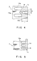
- Figs. 4 and 5 represent the connection land portions 18a and U-shaped openings 14, for a staggered array of tails and to a single non-staggered row of tails respectively.
- a solder paste 20 is printed on the solder pad exposed portions 18 in the U-shaped openings 14 prior to a soldering step.
- the thickness of the solder mask layer 8 is, for example, about 4 mils, the thickness of the solder paste 20 is set to be about 2 to 34 mils.
- Tin-plated solder tails are employed as the solder tails 22 of the contacts of the connector which is to be connected to the connection land portion 18a (see Figs. 4 and 5) of the solder pad 10.
- each solder tail 22 Prior to the soldering step, each solder tail 22 is inserted onto the associated connection land portion 18a in the U-shaped opening 14. That is, the forward end of the solder tail 22 is inserted onto the opening 14 via the edge 4a of the laminated board 4 and hence guided onto the connection land portion 18a along one side edge of the U-shaped opening 14.
- the U-shaped opening 14 serves as a guide area for guiding the solder tail 22 of the connector onto the connection land portion 18a, it is easy to properly orient the solder tail relative to the connection land portion 18a even if the solder tails 22 are arranged as a fine pitch array. Further, any misalignment can be avoided between the solder tail 22 and the connection land portion 18a upon soldering.
- solder tails 22 the connection land portions 18a of the solder pads 10 which are oriented in their position are soldered by, for example, a reflow type automatic soldering apparatus so that they are electrically and mechanically connected to each other.
- solder paste 20 may be coated onto the solder pad exposed portions 18 and, in this case, the solder tails 22 may be soldered to the connection land portion 18a manually.
- molten solder 26 in the respective U-shaped opening 14 is dammed up by the inner wall 16 of the U-shaped opening 14. It is thus possible to prevent leakage of the molten solder into the adjacent U-shaped openings and to prevent the formation of a solder bridge or bridges which might cause a short-circuiting between the adjacent solder tails 22.
- solder pad 10 is not restricted to the ones illustrated and explained above.
Landscapes
- Engineering & Computer Science (AREA)
- Manufacturing & Machinery (AREA)
- Microelectronics & Electronic Packaging (AREA)
- Electric Connection Of Electric Components To Printed Circuits (AREA)
- Multi-Conductor Connections (AREA)
- Coupling Device And Connection With Printed Circuit (AREA)
- Printing Elements For Providing Electric Connections Between Printed Circuits (AREA)
- Non-Metallic Protective Coatings For Printed Circuits (AREA)
Description
- The present invention relates to a printed circuit board and, in particular, to a connector-mount type printed circuit board.
- In a connector-mount printed circuit board the contacts of the connector are each mounted on a solder pad provided over the printed circuit board or the contacts of the connector are each inserted into a corresponding through hole provided in the printed circuit board. That circuit pattern and contacts are soldered for electrical connection.
- Aligning a greater number of contacts accurately with solder pads or through holes prior to a soldering step involves a complex, delicate operation and hence reduces operation efficiency.
- Upon the soldering of the contacts of the connector to the circuit pattern, the contacts are sometimes liable to be soldered to a location misaligned with the solder pad, or cannot be uniformly joined by a soldering step at all times, because the contact is temporarily not set relative to the solder pad. Further, a bridge is sometimes created across those adjacent contacts due to the deposition of excessive solder, thus short-circuiting the contact involved.
- Such a misalignment and short-circuiting occur prominently in those cases, in particular, where the pitch of adjacent contacts is finely set. It is accordingly the object of the present invention to provide a printed circuit board which can readily set contacts in an aligned relation, upon soldering, and ensure a simpler soldering operation for terminal electrical connection without creating any solder bridge or bridges.
- It is known from US-A-4303291 and from JP-A-3241888 (Patent Abstracts of Japan Vol. 16 No. 27) to provide a solder mask layer resistant to solder over a printed circuit pattern layer on a printed circuit board and to remove regions of the solder mask layer to expose solder pads for connection to contacts of a connector.
- As is known from US-A-4303291, the present invention provides a printed circuit board for electrically connecting to a connector having a plurality of contacts comprising:
- a laminated board;
- a conductive printed circuit pattern layer provided over a surface of the laminated board, said circuit pattern layer also defining a plurality of separate solder pads intended for soldering to the contacts and
- a solder mask layer partly covering the circuit pattern layer and the solder pads.
- In contrast to US-A-4303291, and in accordance with the present invention, the solder mark layer has openings facing an edge of the board and corresponding to the solder pads to create exposed portions of the solder pads and the solder mask layer covers all the edge surfaces of the solder pads except for the edge surfaces adjacent the edge of the board and the exposed portions of the solder pads alternate with portions of the solder mask layer, along said one edge of said laminated board.
- The exposed portions of the solder pads may include a plurality of connection land portions intended to be soldered to a corresponding contact or solder tail with the contact placed on the exposed portion of the connection land portion.
- Upon the soldering of the contacts of the connector to the exposed portions of the connection land portions of the solder pads of the printed circuit board, molten solder is dammed up by the inner wall of the solder mask layer interposed between adjacent land portions thus preventing any solder bridge or bridges from being created across the adjacent land portion.
- As the printed circuit board is opened at the one edge, when the contacts are positioned relative to connection land portions prior to the soldering step, the inner wall of the solder mask layer defining the exposed areas of the connection land portions serves as a guide for guiding the contacts onto the connection land portions.
- This invention can be more fully understood from the following detailed description when taken in conjunction with the accompanying drawings, in which
- Fig. 1 is a perspective view showing part of a printed circuit board according to one embodiment of the present invention;
- Fig. 2 is a top view showing the printed circuit board before their mounting together with a connector is performed;
- Fig. 3 is a cross-sectional view as taken along line III - III in Fig. 2;
- Fig. 4 is a top view showing U-shaped openings or recesses and connection land portions for a staggered array of solder tails;
- Fig. 5 is a top view showing U-shaped openings or recesses and connection land portions for a single array of solder tails;
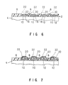
- Fig. 6 is a cross-sectional view showing solder pads and solder tails before a reflow soldering method is carried out;
- Fig. 7 is a cross-sectional view showing the solder pads and solder tails after the reflow soldering method is carried out; and
- Fig. 8 is a cross-sectional view showing a solder pad and solder tail soldered together by a hand soldering operation.
- Figs. 1 to 3 show a printed circuit board according to an embodiment of the present invention.
- The printed
circuit board 2 comprises a laminatedboard 4, a printed circuit pattern layer 6 and a solder mask layer 3 which are sequentially stacked in that order. A connector (not shown) such as a receptacle connector or a header connector with contacts is connected to theprinted circuit board 2. - The circuit pattern layer 6 is formed of a conductive metal, usually copper, and has
solder pads 10 arranged relative to planar connection land portions and acircuit pattern 12. Thesolder pads 10 are arranged along oneedge 4a of the surface of the laminatedboard 4. One of fouredge surfaces 10a, 10b, 10c and 10d of therespective solder pad 10 is situated adjacent theedge 4a of the laminatedboard 4. The width of eachsolder pad 10 in an array direction of thesoldered pads 10 is about two times or more of a solder tail of a corresponding connector to be connected. The surface of thesolder pad 10 is tin-plated. - The
solder mask layer 8 is formed of a dry film solder mask made of, for example, an ultraviolet radiation hardening type photopolymer or a solder resist layer. Thesolder mask layer 8 partly covers the surface of the circuit pattern layer 6. As shown in Fig. 2 in particular, thesolder mask layer 8 has a U-shaped opening in the form of a chamfer or recess 14 at an area of each of thesolder pads 10. The U-shapedopenings 14 serve as guides for guiding contacts of the connector. - The planar configuration of each
U-shaped opening 14 is defined by aninner wall 16 of thesolder mask layer 8 on the surface of thesolder pad 10 and theedge surface 10a which is not covered by eachsolder mask layer 8. Theinner wall 16 of the U-shaped opening 14 covers the three edge surfaces 10b to 10d of the associatedsolder pad 10. Theinner wall 16 of each U-shaped opening 14 serves as a solder dam for preventing molten solder from flowing from the U-shaped opening 14. - The surface of the
solder pad 10 defining the bottom of the U-shapedopening 14 provides an exposedsurface portion 18 not covered with thesolder mask layer 8. - As shown in Fig. 3, the
solder mask layer 8 and solder pad exposedportions 18 are alternately arranged, in a stepped relation, along theedge 4a of the laminatedboard 4. - Figs. 4 and 5 show alternative dispositions for the
connection land portions 18a, that is, the areas where parts of the contacts (the solder tails) of the connector are to be soldered to thesurface portions 18 of thesolder pads 10. Theconnection land portions 18a correspond to the solder pad exposedportions 18 at a surrounded area indicated by the dotted line. - In Fig. 4 the
connection land portions 18a have theiredges 18b situated at one of two predetermined distances L from theedge 4a of the laminatedboard 4. In Fig. 5, theconnection land portions 18a are all disposed at the same distance L from theedge 4a of the laminatedboard 4. - In each U-shaped
opening 14, the area defined by the distance L serves as a guide area for guiding the solder tail onto theconnection land portion 18a. - The detailed configuration of the
U-shaped openings 14, the distance L of the guide areas, the array ofconnection land portions 18a, etc., are determined depending upon the configuration and array of the solder tails of the connector. Thus Figs. 4 and 5 represent theconnection land portions 18a andU-shaped openings 14, for a staggered array of tails and to a single non-staggered row of tails respectively. - Mounting the connector on the printed circuit board constructed as set out above will be explained below in more detail.
- As shown in Fig. 6 a
solder paste 20 is printed on the solder pad exposedportions 18 in the U-shapedopenings 14 prior to a soldering step. Given that the thickness of thesolder mask layer 8 is, for example, about 4 mils, the thickness of thesolder paste 20 is set to be about 2 to 34 mils. - Tin-plated solder tails are employed as the
solder tails 22 of the contacts of the connector which is to be connected to theconnection land portion 18a (see Figs. 4 and 5) of thesolder pad 10. Prior to the soldering step, eachsolder tail 22 is inserted onto the associatedconnection land portion 18a in the U-shaped opening 14. That is, the forward end of thesolder tail 22 is inserted onto theopening 14 via theedge 4a of the laminatedboard 4 and hence guided onto theconnection land portion 18a along one side edge of the U-shaped opening 14. - Since the U-shaped
opening 14 serves as a guide area for guiding thesolder tail 22 of the connector onto theconnection land portion 18a, it is easy to properly orient the solder tail relative to theconnection land portion 18a even if thesolder tails 22 are arranged as a fine pitch array. Further, any misalignment can be avoided between thesolder tail 22 and theconnection land portion 18a upon soldering. - As shown in Fig. 7, the
solder tails 22 theconnection land portions 18a of thesolder pads 10 which are oriented in their position are soldered by, for example, a reflow type automatic soldering apparatus so that they are electrically and mechanically connected to each other. - Alternatively, as shown in Fig. 8, the
solder paste 20 may be coated onto the solder pad exposedportions 18 and, in this case, thesolder tails 22 may be soldered to theconnection land portion 18a manually. - In any case, molten solder 26 in the respective U-shaped opening 14 is dammed up by the
inner wall 16 of the U-shaped opening 14. It is thus possible to prevent leakage of the molten solder into the adjacent U-shaped openings and to prevent the formation of a solder bridge or bridges which might cause a short-circuiting between theadjacent solder tails 22. - Although the present invention has been explained as being one embodiment, it is not restricted to this embodiment. For example, the details of the
solder pad 10, such as its configuration, are not restricted to the ones illustrated and explained above.
Claims (5)
- A printed circuit board (2) for electrically connecting to a connector (24) having a plurality of contacts (22), comprising:a laminated board (4);a conductive printed circuit pattern layer (6,12) provided over a surface of the laminated board (4), said circuit pattern layer also defining a plurality of separate solder pads (10) intended for soldering to the contacts (22) anda solder mask layer (8) partly covering the circuit pattern layer (6) and the solder pads (10);characterised in thatthe solder mask layer (8) has openings (14) facing an edge (4a) of the board (4) and corresponding to the solder pads (10) to create exposed portions (18) of the solder pads (10) and the solder mask layer covers all the edge surfaces (l0b, 10c, l0d) of the solder pads (10) except for the edge surfaces (10a) adjacent the edge (4a) of the board (4) and the exposed portions (18) of the solder pads (10) alternate with portions of the solder mask layer (8), along said one edge (4a) of said laminated board (4).
- A printed circuit board (2) according to claim 1 wherein the exposed portions (18) of the solder pads (10) include a plurality of connection
land portions (18a) each spaced at a pre-determined distance from the edge (4a) of the laminated board (4). - A printed circuit board according to claim 2, wherein the connection land portions (18a) are spaced from the edge (4a) of the board by the same predetermined distance (Figure 5).
- A printed circuit board according to claim 2, wherein the connection land portions (18a) are spaced from the edge (4c) of the board by first and second alternating pre-determined distances (Figure 4).
- A printed circuit board according to any one of claims 1 to 4, wherein the openings (14) in the solder mask layer (8) are U-shaped.
Applications Claiming Priority (2)
| Application Number | Priority Date | Filing Date | Title |
|---|---|---|---|
| JP1992006211U JP2554542Y2 (en) | 1992-02-17 | 1992-02-17 | Printed circuit board |
| JP6211/92U | 1992-02-17 |
Publications (2)
| Publication Number | Publication Date |
|---|---|
| EP0557081A1 EP0557081A1 (en) | 1993-08-25 |
| EP0557081B1 true EP0557081B1 (en) | 1996-04-24 |
Family
ID=11632197
Family Applications (1)
| Application Number | Title | Priority Date | Filing Date |
|---|---|---|---|
| EP93301168A Expired - Lifetime EP0557081B1 (en) | 1992-02-17 | 1993-02-16 | Printed circuit board |
Country Status (5)
| Country | Link |
|---|---|
| US (1) | US5386087A (en) |
| EP (1) | EP0557081B1 (en) |
| JP (1) | JP2554542Y2 (en) |
| KR (1) | KR970005001B1 (en) |
| DE (1) | DE69302296T2 (en) |
Families Citing this family (40)
| Publication number | Priority date | Publication date | Assignee | Title |
|---|---|---|---|---|
| GB2265325A (en) * | 1992-03-18 | 1993-09-29 | Ibm | Solder application to a circuit board |
| JP3147666B2 (en) * | 1994-07-21 | 2001-03-19 | 株式会社村田製作所 | Multilayer electronic component and method of manufacturing the same |
| JP2673098B2 (en) * | 1994-08-03 | 1997-11-05 | インターナショナル・ビジネス・マシーンズ・コーポレイション | Printed wiring board and mounting structure |
| CN1164154C (en) * | 1996-05-31 | 2004-08-25 | 罗姆股份有限公司 | Installation method of terminal on circuit board and circuit board |
| US6803656B2 (en) * | 1997-12-31 | 2004-10-12 | Micron Technology, Inc. | Semiconductor device including combed bond pad opening |
| JPH11220234A (en) * | 1998-01-29 | 1999-08-10 | Smk Corp | Circuit board |
| US6169253B1 (en) | 1998-06-08 | 2001-01-02 | Visteon Global Technologies, Inc. | Solder resist window configurations for solder paste overprinting |
| US6115262A (en) * | 1998-06-08 | 2000-09-05 | Ford Motor Company | Enhanced mounting pads for printed circuit boards |
| US6316736B1 (en) | 1998-06-08 | 2001-11-13 | Visteon Global Technologies, Inc. | Anti-bridging solder ball collection zones |
| DE19836456C1 (en) * | 1998-08-12 | 2000-04-20 | Kostal Leopold Gmbh & Co Kg | Electrical circuit board and method of manufacturing the same |
| US6194667B1 (en) * | 1998-08-19 | 2001-02-27 | International Business Machines Corporation | Receptor pad structure for chip carriers |
| US6078013A (en) * | 1998-10-08 | 2000-06-20 | International Business Machines Corporation | Clover-leaf solder mask opening |
| WO2002071819A1 (en) * | 2001-03-07 | 2002-09-12 | Sony Corporation | Land portion of printed wiring board, method for manufacturing printed wiring board, and printed wiring board mounting method |
| US6583019B2 (en) | 2001-11-19 | 2003-06-24 | Gennum Corporation | Perimeter anchored thick film pad |
| CN1672475B (en) * | 2002-06-27 | 2011-11-23 | Ppg工业俄亥俄公司 | Single or multi-layer printed circuit board with recessed or extended breakaway tabs and method of manufacture thereof |
| JP4060810B2 (en) * | 2004-02-27 | 2008-03-12 | 富士通株式会社 | Recording disk drive device, flexible printed circuit board unit, and flexible printed circuit board |
| JP4709512B2 (en) * | 2004-08-19 | 2011-06-22 | 株式会社東芝 | Electronics |
| JP4734995B2 (en) * | 2005-03-29 | 2011-07-27 | ミツミ電機株式会社 | Land structure, printed wiring board and electronic device |
| US7511228B2 (en) * | 2005-09-14 | 2009-03-31 | Schmartboard, Inc. | Printed circuit board |
| JP2009158892A (en) * | 2007-12-28 | 2009-07-16 | Nec Corp | Multilayer wiring board and method of manufacturing the same |
| US20090260862A1 (en) * | 2008-04-16 | 2009-10-22 | Andrew Yaung | Circuit modification device for printed circuit boards |
| JP5724278B2 (en) * | 2010-09-30 | 2015-05-27 | 大日本印刷株式会社 | Suspension substrate, method for manufacturing suspension substrate, suspension, suspension with element, and hard disk drive |
| US8007291B1 (en) * | 2010-10-15 | 2011-08-30 | International Business Machines Corporation | Implementing differential signal circuit board electrical contact |
| JP6024078B2 (en) * | 2011-08-17 | 2016-11-09 | 大日本印刷株式会社 | Suspension board |
| USD668658S1 (en) * | 2011-11-15 | 2012-10-09 | Connectblue Ab | Module |
| USD668659S1 (en) * | 2011-11-15 | 2012-10-09 | Connectblue Ab | Module |
| USD680545S1 (en) * | 2011-11-15 | 2013-04-23 | Connectblue Ab | Module |
| USD689053S1 (en) * | 2011-11-15 | 2013-09-03 | Connectblue Ab | Module |
| USD680119S1 (en) * | 2011-11-15 | 2013-04-16 | Connectblue Ab | Module |
| USD692896S1 (en) * | 2011-11-15 | 2013-11-05 | Connectblue Ab | Module |
| CN103327728A (en) * | 2012-03-21 | 2013-09-25 | 鸿富锦精密工业(深圳)有限公司 | Printed circuit board |
| DE102013202806B4 (en) * | 2013-01-31 | 2025-07-24 | Rohde & Schwarz GmbH & Co. Kommanditgesellschaft | Circuit on thin substrate for use in waveguides and manufacturing processes |
| JP6152816B2 (en) * | 2014-03-26 | 2017-06-28 | ソニー株式会社 | SEMICONDUCTOR DEVICE, DISPLAY PANEL, DISPLAY DEVICE, ELECTRONIC DEVICE, AND SEMICONDUCTOR DEVICE MANUFACTURING METHOD |
| US9496154B2 (en) | 2014-09-16 | 2016-11-15 | Invensas Corporation | Use of underfill tape in microelectronic components, and microelectronic components with cavities coupled to through-substrate vias |
| CN105828521B (en) * | 2015-01-08 | 2018-10-02 | 上海和辉光电有限公司 | The layout method and printed circuit board of printed circuit board |
| JP6460845B2 (en) * | 2015-03-03 | 2019-01-30 | 日東電工株式会社 | Printed circuit board |
| US10305193B1 (en) * | 2018-02-22 | 2019-05-28 | Raytheon Company | Wide-band high speed communications channel for cryogenic applications |
| US10314162B1 (en) * | 2018-07-13 | 2019-06-04 | Mellanox Technologies, Ltd. | Apparatuses and methods for improved network connections |
| CN112997591B (en) * | 2018-11-08 | 2025-04-01 | 株式会社村田制作所 | Ceramic electronic components |
| US11342697B2 (en) | 2020-06-04 | 2022-05-24 | International Business Machines Corporation | Dual-level pad card edge self-guide and alignment of connector |
Citations (1)
| Publication number | Priority date | Publication date | Assignee | Title |
|---|---|---|---|---|
| US4303291A (en) * | 1980-11-24 | 1981-12-01 | Western Electric Company, Inc. | Method of seating connector terminals on circuit board contact pads |
Family Cites Families (12)
| Publication number | Priority date | Publication date | Assignee | Title |
|---|---|---|---|---|
| JPS5137265U (en) * | 1974-09-11 | 1976-03-19 | ||
| US4132341A (en) * | 1977-01-31 | 1979-01-02 | Zenith Radio Corporation | Hybrid circuit connector assembly |
| US4295183A (en) * | 1979-06-29 | 1981-10-13 | International Business Machines Corporation | Thin film metal package for LSI chips |
| JPS60133656U (en) * | 1984-02-14 | 1985-09-06 | 株式会社東芝 | flexible printed wiring board |
| US4755631A (en) * | 1985-04-11 | 1988-07-05 | International Business Machines Corporation | Apparatus for providing an electrical connection to a metallic pad situated on a brittle dielectric substrate |
| JPS6292679U (en) * | 1985-11-29 | 1987-06-13 | ||
| JPS62184785U (en) * | 1986-05-16 | 1987-11-24 | ||
| JPH0160464U (en) * | 1987-10-09 | 1989-04-17 | ||
| US4893216A (en) * | 1988-08-09 | 1990-01-09 | Northern Telecom Limited | Circuit board and method of soldering |
| US4965702A (en) * | 1989-06-19 | 1990-10-23 | E. I. Du Pont De Nemours And Company | Chip carrier package and method of manufacture |
| JPH0423485A (en) * | 1990-05-18 | 1992-01-27 | Cmk Corp | Printed wiring board and manufacture thereof |
| JPH105096A (en) * | 1996-06-24 | 1998-01-13 | Shinichi Sakamoto | Instrument for preventing mat or quilt from being displaced |
-
1992
- 1992-02-17 JP JP1992006211U patent/JP2554542Y2/en not_active Expired - Fee Related
-
1993
- 1993-02-16 EP EP93301168A patent/EP0557081B1/en not_active Expired - Lifetime
- 1993-02-16 KR KR1019930002119A patent/KR970005001B1/en not_active Expired - Fee Related
- 1993-02-16 US US08/017,921 patent/US5386087A/en not_active Expired - Fee Related
- 1993-02-16 DE DE69302296T patent/DE69302296T2/en not_active Expired - Fee Related
Patent Citations (1)
| Publication number | Priority date | Publication date | Assignee | Title |
|---|---|---|---|---|
| US4303291A (en) * | 1980-11-24 | 1981-12-01 | Western Electric Company, Inc. | Method of seating connector terminals on circuit board contact pads |
Also Published As
| Publication number | Publication date |
|---|---|
| JP2554542Y2 (en) | 1997-11-17 |
| DE69302296D1 (en) | 1996-05-30 |
| DE69302296T2 (en) | 1996-09-12 |
| KR970005001B1 (en) | 1997-04-10 |
| US5386087A (en) | 1995-01-31 |
| KR930019079A (en) | 1993-09-22 |
| JPH0593069U (en) | 1993-12-17 |
| EP0557081A1 (en) | 1993-08-25 |
Similar Documents
| Publication | Publication Date | Title |
|---|---|---|
| US5386087A (en) | Printed circuit board having U-shaped solder mask layer separating respective contacts | |
| EP0516402B1 (en) | Substrate provided with electric lines and its manufacturing method | |
| US6115262A (en) | Enhanced mounting pads for printed circuit boards | |
| US4303291A (en) | Method of seating connector terminals on circuit board contact pads | |
| GB2080629A (en) | Printed circuit boards | |
| EP0696159A1 (en) | Printed wiring board | |
| EP0059337B1 (en) | High density connecting system and method for semi-conductor devices | |
| EP0531126B1 (en) | Pattern structure of a printed circuit board | |
| EP0332747B1 (en) | Tape automated bonding package | |
| JPH0219635B2 (en) | ||
| US5132864A (en) | Printed circuit board | |
| JP3509239B2 (en) | Leadless chip carrier and manufacturing method thereof | |
| JPH0832195A (en) | Connection structure of composite printed board | |
| KR100246360B1 (en) | Microvisie Package | |
| JPS5848492A (en) | Flexible printed wiring board and its solder connection method | |
| JPH0345543B2 (en) | ||
| JP4303833B2 (en) | Multiple chip resistor and manufacturing method thereof | |
| JP3004397B2 (en) | Flexible printed circuit board | |
| JPH07235636A (en) | Semiconductor device and laminated structure thereof | |
| JP2528436B2 (en) | Manufacturing method of circuit board device | |
| JP3416207B2 (en) | Flexible printed circuit board | |
| JP2025074819A (en) | Connectors and Connector Units | |
| JPH0144034B2 (en) | ||
| JP2025081088A (en) | Connectors and Connector Units | |
| CN119401156A (en) | Electrical connector |
Legal Events
| Date | Code | Title | Description |
|---|---|---|---|
| PUAI | Public reference made under article 153(3) epc to a published international application that has entered the european phase |
Free format text: ORIGINAL CODE: 0009012 |
|
| AK | Designated contracting states |
Kind code of ref document: A1 Designated state(s): DE FR GB |
|
| 17P | Request for examination filed |
Effective date: 19930726 |
|
| 16A | New documents despatched to applicant after publication of the search report | ||
| 17Q | First examination report despatched |
Effective date: 19940620 |
|
| RAP1 | Party data changed (applicant data changed or rights of an application transferred) |
Owner name: CONNECTOR SYSTEMS TECHNOLOGY N.V. |
|
| GRAH | Despatch of communication of intention to grant a patent |
Free format text: ORIGINAL CODE: EPIDOS IGRA |
|
| GRAA | (expected) grant |
Free format text: ORIGINAL CODE: 0009210 |
|
| AK | Designated contracting states |
Kind code of ref document: B1 Designated state(s): DE FR GB |
|
| ET | Fr: translation filed | ||
| REF | Corresponds to: |
Ref document number: 69302296 Country of ref document: DE Date of ref document: 19960530 |
|
| PLBE | No opposition filed within time limit |
Free format text: ORIGINAL CODE: 0009261 |
|
| STAA | Information on the status of an ep patent application or granted ep patent |
Free format text: STATUS: NO OPPOSITION FILED WITHIN TIME LIMIT |
|
| 26N | No opposition filed | ||
| REG | Reference to a national code |
Ref country code: GB Ref legal event code: 732E |
|
| REG | Reference to a national code |
Ref country code: FR Ref legal event code: TP |
|
| REG | Reference to a national code |
Ref country code: GB Ref legal event code: IF02 |
|
| PGFP | Annual fee paid to national office [announced via postgrant information from national office to epo] |
Ref country code: GB Payment date: 20030106 Year of fee payment: 11 |
|
| PGFP | Annual fee paid to national office [announced via postgrant information from national office to epo] |
Ref country code: FR Payment date: 20030204 Year of fee payment: 11 |
|
| PGFP | Annual fee paid to national office [announced via postgrant information from national office to epo] |
Ref country code: DE Payment date: 20030228 Year of fee payment: 11 |
|
| PG25 | Lapsed in a contracting state [announced via postgrant information from national office to epo] |
Ref country code: GB Free format text: LAPSE BECAUSE OF NON-PAYMENT OF DUE FEES Effective date: 20040216 |
|
| PG25 | Lapsed in a contracting state [announced via postgrant information from national office to epo] |
Ref country code: DE Free format text: LAPSE BECAUSE OF NON-PAYMENT OF DUE FEES Effective date: 20040901 |
|
| GBPC | Gb: european patent ceased through non-payment of renewal fee |
Effective date: 20040216 |
|
| PG25 | Lapsed in a contracting state [announced via postgrant information from national office to epo] |
Ref country code: FR Free format text: LAPSE BECAUSE OF NON-PAYMENT OF DUE FEES Effective date: 20041029 |
|
| REG | Reference to a national code |
Ref country code: FR Ref legal event code: ST |