EP0556074B1 - Magnetic head driving circuit - Google Patents
Magnetic head driving circuit Download PDFInfo
- Publication number
- EP0556074B1 EP0556074B1 EP93400084A EP93400084A EP0556074B1 EP 0556074 B1 EP0556074 B1 EP 0556074B1 EP 93400084 A EP93400084 A EP 93400084A EP 93400084 A EP93400084 A EP 93400084A EP 0556074 B1 EP0556074 B1 EP 0556074B1
- Authority
- EP
- European Patent Office
- Prior art keywords
- magnetic field
- magnetic head
- driving circuit
- field generating
- fet
- Prior art date
- Legal status (The legal status is an assumption and is not a legal conclusion. Google has not performed a legal analysis and makes no representation as to the accuracy of the status listed.)
- Expired - Lifetime
Links
Images


Classifications
-
- G—PHYSICS
- G11—INFORMATION STORAGE
- G11B—INFORMATION STORAGE BASED ON RELATIVE MOVEMENT BETWEEN RECORD CARRIER AND TRANSDUCER
- G11B11/00—Recording on or reproducing from the same record carrier wherein for these two operations the methods are covered by different main groups of groups G11B3/00 - G11B7/00 or by different subgroups of group G11B9/00; Record carriers therefor
- G11B11/10—Recording on or reproducing from the same record carrier wherein for these two operations the methods are covered by different main groups of groups G11B3/00 - G11B7/00 or by different subgroups of group G11B9/00; Record carriers therefor using recording by magnetic means or other means for magnetisation or demagnetisation of a record carrier, e.g. light induced spin magnetisation; Demagnetisation by thermal or stress means in the presence or not of an orienting magnetic field
- G11B11/105—Recording on or reproducing from the same record carrier wherein for these two operations the methods are covered by different main groups of groups G11B3/00 - G11B7/00 or by different subgroups of group G11B9/00; Record carriers therefor using recording by magnetic means or other means for magnetisation or demagnetisation of a record carrier, e.g. light induced spin magnetisation; Demagnetisation by thermal or stress means in the presence or not of an orienting magnetic field using a beam of light or a magnetic field for recording by change of magnetisation and a beam of light for reproducing, i.e. magneto-optical, e.g. light-induced thermomagnetic recording, spin magnetisation recording, Kerr or Faraday effect reproducing
- G11B11/10502—Recording on or reproducing from the same record carrier wherein for these two operations the methods are covered by different main groups of groups G11B3/00 - G11B7/00 or by different subgroups of group G11B9/00; Record carriers therefor using recording by magnetic means or other means for magnetisation or demagnetisation of a record carrier, e.g. light induced spin magnetisation; Demagnetisation by thermal or stress means in the presence or not of an orienting magnetic field using a beam of light or a magnetic field for recording by change of magnetisation and a beam of light for reproducing, i.e. magneto-optical, e.g. light-induced thermomagnetic recording, spin magnetisation recording, Kerr or Faraday effect reproducing characterised by the transducing operation to be executed
- G11B11/10504—Recording
- G11B11/10508—Recording by modulating only the magnetic field at the transducer
-
- G—PHYSICS
- G11—INFORMATION STORAGE
- G11B—INFORMATION STORAGE BASED ON RELATIVE MOVEMENT BETWEEN RECORD CARRIER AND TRANSDUCER
- G11B11/00—Recording on or reproducing from the same record carrier wherein for these two operations the methods are covered by different main groups of groups G11B3/00 - G11B7/00 or by different subgroups of group G11B9/00; Record carriers therefor
- G11B11/10—Recording on or reproducing from the same record carrier wherein for these two operations the methods are covered by different main groups of groups G11B3/00 - G11B7/00 or by different subgroups of group G11B9/00; Record carriers therefor using recording by magnetic means or other means for magnetisation or demagnetisation of a record carrier, e.g. light induced spin magnetisation; Demagnetisation by thermal or stress means in the presence or not of an orienting magnetic field
- G11B11/105—Recording on or reproducing from the same record carrier wherein for these two operations the methods are covered by different main groups of groups G11B3/00 - G11B7/00 or by different subgroups of group G11B9/00; Record carriers therefor using recording by magnetic means or other means for magnetisation or demagnetisation of a record carrier, e.g. light induced spin magnetisation; Demagnetisation by thermal or stress means in the presence or not of an orienting magnetic field using a beam of light or a magnetic field for recording by change of magnetisation and a beam of light for reproducing, i.e. magneto-optical, e.g. light-induced thermomagnetic recording, spin magnetisation recording, Kerr or Faraday effect reproducing
- G11B11/10532—Heads
- G11B11/10534—Heads for recording by magnetising, demagnetising or transfer of magnetisation, by radiation, e.g. for thermomagnetic recording
- G11B11/10536—Heads for recording by magnetising, demagnetising or transfer of magnetisation, by radiation, e.g. for thermomagnetic recording using thermic beams, e.g. lasers
Definitions
- This invention relates to a magnetic head device employed in a magneto-optical disc system and a magnetic head driving circuit for driving and controlling the magnetic head device. More particularly, it relates to a magnetic head device employed for recording information signals on a magneto-optical disc and a magnetic head driving circuit for controlling the driving current driving the magnetic head device.
- a disc recording apparatus comprising an optical pickup device for radiating a light beam to a magneto-optical disc and detecting the return light from the magneto-optical disc and a magnetic head device arranged facing the optical pickup device for applying an external magnetic field to the magneto-optical disc, in which the magneto-optical disc is rotationally driven between the optical pickup device and the magnetic head device for recording information signals on the disc.
- recording of information signals on the magneto-optical disc is carried out by radiating a converged light beam from the optical pickup device on a signal recording layer of the magneto-optical disc for heating the recording layer and by applying an external magnetic field by the magnetic head device on the heated portion of the signal recording layer for aligning the direction of magnetization of the heated portion with the direction of the external magnetic field applied by the magnetic head device.
- the magnetic head device employed in the above-described disc recording apparatus comprises a magnetic field generating coil which is supplied with a driving current controlled by a magnetic head driving circuit for generating a magnetic field.
- the magnetic head driving circuit controls the driving current in accordance with information signals to be recorded on the magneto-optical disc for modulating the magnetic field generated by the magnetic field generating coil in accordance with the information signals.
- the magnetic head device is controlled in movement to follow the magneto-optical disc so that it is always spaced apart from the surface of the signal recording layer of the magneto-optical disc at a distance of approximately 100 ⁇ m to 200 ⁇ m.
- This movement is realized by providing a sheet of a uniform thickness on the surface of the signal recording layer and moving the magnetic head device on and in sliding contact with the sheet surface.
- a magnetic head driving circuit 114 comprises a plurality of field effect transistors (FETs) as switching elements, as shown in Fig.1.
- the magnetic head driving circuit 114 is connected to a logic circuit 113 supplied with clock signals and recording signals which are the above-mentioned information signals to be recorded on the signal recording layer 103.
- the magnetic head driving circuit 114 comprises first to sixth FETs 115 to 120 having their gate terminals connected to the logic circuit 113 so as to be turned on and off by the logic circuit 113.
- the first and second FETs 115, 116 are P-channel FETs, while the third to sixth FETs 117 to 120 are N-channel FETs.
- a positive power source +V is connected to drain terminals of the first and second FETs 115, 116.
- the first FET 115 has its source terminal connected to a source terminal of the third FET 117 and also connected to a drain terminal of the fourth FET 117 via a first diode 121.
- the second FET 116 has its source terminal connected to a source terminal of the fifth FET 119 and also connected to a drain terminal of the sixth FET 120 via a second diode 122.
- a magnetic field generating coil L is connected across the source terminal of the first FET 115 and the source terminal of the second FET 116.
- the third and fifth FETs 117, 119 have their drain terminals connected to a negative power source -V, while the fourth and sixth FETs 118, 120 have their drain terminals connected to ground potential.
- the first FET 115 which has been turned on when the recording signal is at a low "L” level
- the second FET 116 which has been turned off when the recording signal is at a low "L” level
- the third FET 117 is turned on during a one-pulse period, based on the clock signals, after the recording signal has gone low.
- the fourth FET 118 is turned on in a pulsed fashion, based on the clock signals, during the period when the recording signal is at the H level, so as to follow up with the third FET 117.
- the first FET 115 which has been turned off when the recording signal is at the high "H” level
- the second FET 116 which has been turned on when the recording signal is at the high "H” level
- the fifth FET 119 is turned on during a one-pulse period, based on the clock signals, after the recording signal has gone low.
- the sixth FET 120 is turned on in a pulsed fashion, based on the clock signals, during the period when the recording signal is at the L level, so as to follow up with the fifth FET 119.
- the voltage V A applied across the magnetic field generating coil L, is changed from +V to -v after the recording signal has gone high and during the time when the third FET 117 is in a turned-on state. Since then, the voltage V A is pulsed in such manner that it is zero and at +V when the fourth FET 118 is in the turned-on state and in the turned-off state, respectively. When the recording signal goes low, the voltage V A is maintained at +V.
- a current I H flowing through the magnetic field generating coil L is maintained at a substantially constant negative value as long as the recording signal is at an H level, and is maintained at a substantially constant positive value as long as the recording signal is at an L level.
- the above-described magnetic head driving circuit can be reduced in size only with difficulty because of the large number of components making up the driving circuit.
- it is necessary to employ a complicated control circuit for controlling the magnetic head driving circuit because of the large number of elements turned on and off in controlled manner.
- the complicated magnetic head driving circuit is employed in the prior art because it has been necessary to increase the magnetic field generated by the magnetic field generating coil L to a sufficiently high level. That is, in view of characteristics of the signal recording layer of the magneto-optical disc, it has been necessary with the prior art driving circuit to apply a sufficiently large magnetic field even if the magnetic head device is spaced apart from the signal recording layer by a distance on the order of 400 ⁇ m.
- a magnetic head driving circuit for driving a magnetic head device adapted for recording information signals on a magneto-optical disc by applying a magnetic field thereto, comprising a pair of switching elements for performing a push-pull operation in accordance with input recording signals, a pair of rectifiers connected in series with each other between said switching elements, a magnetic field generating coil having its one terminal connected to a junction line between said rectifying elements via a coupling capacitor and having its other terminal grounded, said magnetic field generating coil generating a magnetic field by being supplied with a driving current corresponding to said recording signals, and an amplifier capacitor connected in parallel with said magnetic field generating coil in an ac path for amplifying said driving current supplied to said magnetic field generating coil.
- the capacitor for amplifying the driving current connected in parallel with the magnetic field generating coil in an ac path, stores the energy of recording signals, and releases the energy on inversion of the recording signals, for amplifying the driving current supplied to the magnetic field generating coil and augmenting the magnetic field generated by the magnetic field generating coil.
- a magnetic head driving circuit according to claim 1.
- the driving circuit is formed of a novel stacked ceramic thin sheet construction forming both the core of a magnetic head and a driving circuit including a coupling capacitor.
- JP-A-2 235 241 a stacked ceramic thin sheet construction has been used in the past (JP-A-2 235 241) for forming a coil, but not for forming a whole magnetic head and a coupling capacitor.
- the present invention also relates to a magnetic head device employing such a driving circuit.
- Fig. 1 is a circuit diagram showing a constitution of a conventional magnetic head driving circuit.
- Fig.2 is a timing chart for illustrating the relation between recording signals, electrical voltage applied across a magnetic field generating coil and the current flowing through the coil in the magnetic head driving circuit shown in Fig.1.
- Fig.3 is a perspective view showing the constitution of essential parts of a recording apparatus employing the magnetic head device according to the present invention.
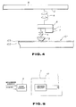
- Fig.4 is an enlarged side view showing an equivalent constitution of the magnetic head device of the present invention.
- Fig.5 is a block circuit diagram of a magnetic head device inclusive of a magnetic head driving circuit according to the present invention.
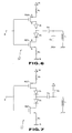
- Fig.6 is a circuit diagram showing a constitution of a magnetic head driving circuit according to the present invention.
- Fig.7 is a circuit diagram showing another constitution of a magnetic head driving circuit according to the present invention.
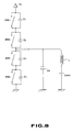
- Fig.8 is a circuit diagram showing an equivalent circuit of a magnetic head driving circuit shown in Fig.6.
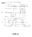
- Fig.9 is a timing chart for illustrating the relation between recording signals, electrical voltage applied across a magnetic field generating coil and the current flowing through the coil in the magnetic head driving circuit shown in Fig.6.
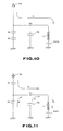
- Fig.10 is a circuit diagram showing an initial state in which the recording signal in the equivalent circuit of Fig.8 is at a low level.
- Fig.11 is a circuit diagram showing the state in which the recording signal in the equivalent circuit of Fig.8 goes high.
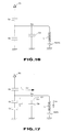
- Fig.12 is a circuit diagram showing the state when the energy of the magnetic field generating coil in the equivalent circuit of Fig.8 is reduced to zero.
- Fig.13 is a circuit diagram showing the state after the energy of the magnetic field generating coil in the equivalent circuit of Fig.8 has been reduced to zero.
- Fig.14 is a circuit diagram showing the state when the energy of the magnetic field generating coil in the equivalent circuit of Fig.8 is at a ground level.
- Fig.15 is a circuit diagram showing the state when the recording signal in the equivalent circuit of Fig.8 is at an L level.
- Fig.16 is a circuit diagram showing the state when, after the recording signal in the equivalent circuit of Fig.8 has gone low, the energy in the magnetic field generating coil is reduced to zero.
- Fig.17 is a circuit diagram showing the state when, after the recording signal in the equivalent circuit of Fig.8 has gone low, the current in a reverse direction starts to flow in the magnetic field generating coil.
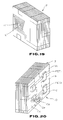
- Fig.19 is an enlarged perspective view showing another example of the constitution of a magnetic head device according to the present invention.
- Fig.20 is an enlarged perspective view, looking from another viewing direction, of the magnetic head device shown in Fig.19.
- Fig.21 is an exploded perspective view showing the constitution of the magnetic head device shown in Fig.19.
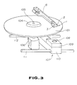
- a magnetic head driving circuit according to the present invention is applied to a recording apparatus in which an optical pickup device 107 and a magnetic head device 1 are arranged with a magneto-optical disc 101 therebetween for recording information signals on the magneto-optical disc 101, as shown in Fig.3.
- the magneto-optical disc 101 comprises a disc substrate 102 and a signal recording layer 103 deposited on the disc substrate 102, as shown in Fig.4.
- the magneto-optical disc 101 is rotationally driven by a spindle motor 106 at a position between the optical pickup device 107 and the magnetic head device 1, while a converged light beam is radiated on the signal recording layer 103 through the light-transmitting disc substrate 102 by the optical pickup device 107, at the same time that an external magnetic field is applied to the signal recording layer 103 by the magnetic head device 1.
- the signal recording layer 103 of the magneto-optical disc 101 is heated in this manner by radiation of the light beam from the optical pickup device 107, while it is supplied with the external magnetic field from the magnetic head device 1, the coercive force of the heated portion is lost and the direction of magnetization of the heated portion is aligned with the direction of the external magnetic field.
- the magneto-optical disc 101 is supported via a chucking unit 104 by a driving shaft 105 of the spindle motor 106.
- the optical pickup device 107 radiating the light beam to the magneto-optical disc, is made up of an optical block 110 and an object lens driving unit 109.
- the optical block 110 has enclosed therein a light source, such as a laser diode, an optical device for guiding the light beam radiated from the light source and a photodetector for receiving the return light beam reflected back from the magneto-optical disc 101.
- the object lens driving unit 109 supports an object lens 108, adapted for converging the light beam from the light source, incident thereon, so that the object lens may be moved in a direction along its optical axis and in a direction normal to the optical axis.
- the object lens driving unit 109 controls the object lens 108 so that the object lens 108 is moved to follow eccentricities or deviations from horizontal of the magneto-optical disc 101 for continuously locating the point of convergence of the light beam by the object lens 108 on the surface of the signal recording layer 103 of the magneto-optical disc 101.
- the optical pickup device 107 is movably supported by a pair of guide shafts 111, 112 for causing the object lens 108 to face the magneto-optical disc 101, supported by a chucking unit 104, across the inner and outer peripheries of the disc 101.
- the magnetic head device 1 adapted for applying the external magnetic field to the magneto-optical disc 101, includes a magnetic field generating coil L, which is fed with a driving current I H controlled by the magnetic head driving circuit, for generating the external magnetic field.
- the magnetic head device 1 is made up of a head support 6 and a circuit part 7 mounted on the head support, as shown in Fig.4.
- the head support 6 is mounted via a compression spring 4 on a distal end 2 of a supporting arm 8 mounted facing the magneto-optical disc 101 for movement between the inner and outer rims of the disc.
- the magnetic head device 1 is pressed against the magneto-optical disc 101 with a predetermined pressure by the compression spring 4.
- a slider 3 is mounted via a damper spring 5 on the head support 6.
- the slider 3 is kept in sliding contact with the surface of the magneto-optical disc 101 on which the signal recording layer 103 is formed.
- the damper spring 5 the magnetic head device 1 is floated by a distance on the order of 100 ⁇ m from the surface of the magneto-optical disk 101 on which the signal recording layer 103 is formed.
- the circuit part 7 is made up of a magnetic head generating coil L and a driving circuit 10 which is a magnetic head driving circuit connected to the coil L, as shown in Fig.5.
- the driving circuit 10 is controlled by a logic circuit 9 supplied with clock signals and recording signals, which are the information signals to be recorded on the magneto-optical disc 101, for controlling the driving current I H in accordance with the recording signals for modulating the external magnetic field in accordance with the recording signals.
- the magnetic head device 1 causes the recording signals to be recorded on the magneto-optical disc 101 in accordance with the so-called magnetic field modulation system.
- the driving circuit 10 has first and second switching elements FET 1 , FET 2 , having their gate terminals connected to an input terminal S supplied with the input recording signals, as shown in Fig.6. These switching elements FET 1 , FET 2 are paired and perform a push-pull operation in accordance with the recording signals. That is, the first and second switching elements FET 1 , FET 2 are field effect transistors, with the first switching element FET 1 being a P-channel FET and the second switching element FET 2 being an N-channel FET. The first switching element FET 1 is turned off and on when the recording signal is at the H and L levels, respectively. Conversely, the second switching element FET 2 is turned on and off when the recording signal is at the H and L levels, respectively.
- a power source V C is connected to a drain terminal of the first switching element FET 1 via a first limiting resistor R 1 ,
- the first switching element FET 1 has its source terminal connected to a drain terminal of the second switching element FET 2 via first and second diodes D 1 , D 2 forming a rectifier.
- the first and second diodes D 1 , D 2 are connected in series with each other, with the direction from the source terminal of the first switching element FET 1 to the drain terminal of the second switching element FET 2 being the forward direction.
- the second switching element FET 2 has its source terminal grounded via a second limiting resistor R 2 .
- the magnetic field generating coil L has one end connected to a junction between the first diode D 1 and the second diode D 2 via a coupling capacitor C C , while having its other end grounded.
- a buffer capacitor C B which is to be a capacitor for amplifying the driving current supplied to the coil L, is connected in parallel with the coil L in an ac path.
- the buffer capacitor C B has one terminal connected to one end of the coil L and had its other terminal grounded.
- the buffer capacitor C B may have one terminal connected to the power source V C and its other terminal connected to one end of the coil L as shown in Fig.7.
- the driving circuit 10 shown in Fig.6 becomes a circuit having first to fourth capacitors C 1 , C 2 , C 3 and C 4 , connected in series with the power source V C , as shown in Fig.8.
- First to fourth switches SW 1 , SW 2 , SW 3 and SW 4 are connected in parallel with the first to fourth capacitors C 1 , C 2 , C 3 and C 4 , respectively.
- the first capacitor C 1 and the first switch SW 1 correspond to the first switching element FET 1 .
- the second capacitor C 2 and the second switch SW 2 correspond to the first diode D 1 .
- the third capacitor C 3 and the third switch SW 3 correspond to the second diode D 2 .
- the fourth capacitor C 4 and the fourth switch SW 4 correspond to the second switching element FET 2 . That is, these first and second switching elements FET 1 , FET 2 may be thought of as having feedback shunt capacitances and being operated as switcnes changed over between the turned-on and turned-off states in accordance with the recording signals.
- first and second switching elements FET 1 , FET 2 are shorted when in the turned-on state, while being operated as feedback capacitances when in the turned-off state.
- the first and second diodes D 1 , D 2 may be thought of as being switching elements switched between the turned-on state and the turned-off state depending on the voltage direction of gradients across capacitor terminals and hence as having parallel capacitances across the capacitor terminals, as in the case of the first and second switching elements FET 1 , FET 2 .
- the magnetic field generating coil L has one terminal connected to a junction line between the second and third capacitors C 2 and C 3 , while having its other terminal connected to an offset voltage source V OFS , which has its anode connected to the magnetic field generating coil L and has its cathode grounded.
- the buffer capacitor C B has its one terminal connected to one terminal of the coil L and has its other terminal grounded.
- the operation of the driving circuit 10 is hereinafter explained by referring to the equivalent circuit shown in Fig. 8.
- the gate terminals of the first and second switching elements FET 1 , FET 2 are at the L level.
- the first switching element FET 1 is turned on to render the first capacitor C 1 inoperative
- the second switching element FET 2 is turned off to render the fourth capacitor C 4 operative, as shown in Fig.10.
- the first diode D 1 is forward biased and hence turned on so that the second capacitor C 2 is rendered inoperative.
- the second diode D 2 is reverse biased and hence turned off so that the third capacitor C 3 is rendered operative.
- the offset power source V OFS of the magnetic field generating coil L is connected alternately to power source V C and to ground via the magnetic field generating coil L.
- the proportions of the connecting time durations is constant at a cycle time width longer than a predetermined cycle time. For example, if the recording signals are modulated by EFM as used in the compact disc, the offset voltage has a switching rate of 10 ⁇ sec and the duty ratio of 1/2, so that the offset voltage is smoothed by the power source and proves to be a constant voltage source V OFS .
- the voltage at a terminal of the magnetic field generating coil L is equal to the voltage of the power source V C , if the sufficiently small threshold voltage is disregarded.
- the voltages of the power source V C and the offset voltage source V OFS are applied to the coil L.
- the driving current I H flows in a negative-going direction through the coil L from one terminal of the coil L towards the offset power source V OFS , as shown by arrow I 1 , with the current quantity being gradually increased in the negative-going direction.
- the energy in the form of the magnetic flux is stored in the magnetic field generating coil L.
- the gate terminals of the first and second switching elements FET 1 , FET 2 are at H level, so that, in the equivalent circuit shown in Fig.8, the first switching element FET 1 is turned off to render the first capacitor C 1 operative, while the second switching element FET 2 is turned on to render the fourth capacitor C 4 inoperative, as shown in Fig.11.
- the states of the first and second capacitors D 1 , D 2 are maintained.
- the coil L tends to cause the current to flow in the same direction as before by the energy stored as the magnetic flux.
- the electrical charges for maintaining the current are supplied to the first and third capacitors C 1 , C 3 and to the buffer capacitor C B , as shown by arrows I 1 , I 2 and I 3 in Fig. 11, so that the voltage V H at one terminal of the magnetic field generating coil L is lowered.
- the driving current I H flowing through the coil L initially flows in the same direction as before, and is subsequently decreased gradually because of energy consumption due to charge migration.
- the voltage V H at one end of the magnetic field generating coil L is decreased to a minimum value V -P , as shown at T 3 in Fig.9.
- the driving current I H is reduced at this time to zero, as shown in Fig.12.
- the maximum energies are stored in the first and third capacitors C 1 , C 3 and in the buffer capacitor C 8 . That is the energy equal to C 1 ⁇ V C (V -P ⁇ is stored in the first capacitor C 1 .
- the energy equal to C B (V -P ) is stored in the buffer capacitor C B .
- C 1 , C 3 and C B are the capacitances of the first and third capacitors C 1 and C 3 and the buffer capacitor C B , respectively.
- the driving current I H is inverted to the positive-going direction, in accordance with a difference in electrical potential between the offset voltage V OFS and the minimum value V -P of the voltage V H at a terminal of the magnetic field generating coil L, as indicated by arrow T 4 in Fig.9. Then, in the equivalent circuit, shown in Fig.8, the first diode D 1 is turned off because the voltage across its terminals is inverted, so that the second capacitor C 2 comes into operation, as shown in Fig.13.
- the current ⁇ i supplied from the second capacitor C 2 , is minute current and hence may be disregarded.
- the gate voltages of the first and second switching elements FET 1 and FET 2 are at L level, so that, in the equivalent circuit, shown in Fig.8, the first switching element FET 1 is turned on to render the first capacitor C 1 inoperative, while the second switching element FET 2 is turned off to render the fourth capacitor C 4 operative, as shown in Fig.15.
- electric charges stored in coil L are transferred to second and fourth capacitors C 2 , C 4 and to buffer capacitor C B , as indicated by arrows I 9 , I 10 and I 11 in Fig.15.
- the driving current I H is flowing in the positive-going direction through the magnetic field generating coil L, as indicated by arrow I 7 in Fig.15, while the voltage V H at one terminal of the magnetic field generating coil L is increased.
- the driving current I H becomes zero, as shown in Figs.16 and 9, while the voltage V H at one terminal of the magnetic field generating coil L reaches a maximum value V P .
- the maximum energies are stored in the second and fourth capacitors C 2 , C 4 and in the buffer capacitor C B . That is, the energy equal to C 2 (V P - V C ) is stored in the second capacitor C 2 , while the energies equal to C 4 V P and C B V P are stored in the fourth capacitor C 4 and buffer capacitor C B , respectively.
- C 2 , C 4 are the capacitances of the second and fourth capacitors C 2 , C 4 , respectively.
- a voltage equal to (V P - V OFS ) is applied across both terminals of the magnetic field generating coil L.
- the effective current I -E I P ⁇ C 2 / (C 2 + C 4 )
- C ⁇ is the sum of the capacitances of the third and fourth capacitors C 3 , C 4 and the buffer capacitor C B and L is the inductance of the magnetic field generating coil L.
- the capacitance C ⁇ is approximately 26 pF. Since the sum of the capacitances C 3 , C 4 is on the order of 10 pF, an optimum value of the capacitance of the buffer capacitor C B is on the order of 16 pF.
- the first and second limiting resistors R 1 , R 2 of the above-mentioned driving circuit 10 limit the time rate of charging to the capacitors C 1 , C 2 , C 3 , C 4 and C B in the equivalent circuit shown in Fig.8 for inhibiting any adverse effects which the errors in characteristics of electronic elements of the driving circuit 10 might have on the characteristics of the driving circuit 10.
- the buffer capacitor C B not only amplifies the driving current I H but also inhibits adverse effects which the errors in characteristics of electronic elements of the driving circuit 10 might have on the characteristics of the driving circuit 10.
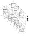
- the magnetic head device according to the present invention is constituted by stacking plural ceramic thin sheets 12, as shown in Figs.19 to 21.
- Each of the ceramic thin sheets 12, making up the substrate 7, has embedded therein a magnetic material constituting the magnetic core 11, a conductor material constituting an interconnection pattern, a spirally-shaped conductor material, constituting the magnetic field generating coil L, a conductor material 16 constituting the coupling capacitor C C and a dielectric material 17, as shown in Fig.21.
- Each ceramic thin sheet 12 also has through-holes 13, 14, 15 for providing connection between the spirally-shaped conductor materials constituting the magnetic field generating coil L.
- the ceramic thin sheets 12 are stacked and sintered together to form a pillar-shaped magnetic core part 11, the magnetic field generating coil L wound around the core part 11, the coupling capacitor C C and the interconnection pattern, as shown in Figs.19 and 20.
- the magnetic field generating coil L is constituted by the spirally-shaped conductor materials connected via through-holes 13, 14, 15.
- the coupling capacitor C C has a conductor sheet integrated to the conductor material 16 which is to be an electrode part at one end, a dielectric member 17 and a conductor sheet integrated to the conductor material 16 as the electrode part at the other end. That is, the electrode parts of the coupling capacitor C C are comb-shaped with the comb teeth being alternately engaged with one another via the dielectric material 17.
- the interconnection pattern is constituted by the conductor materials facing the outer lateral sides of the substrate 7 formed by the thin ceramic sheets 12 for providing connection between the magnetic field generating coil L and the coupling capacitor C C while providing predetermined pattern of the power source pattern V C , input terminal pattern S or the grounding pattern G.
- the first and second switching elements FET 1 , FET 2 , first and second diodes D 1 , D 2 and buffer capacitor C B , formed as chip components, are mounted on the substrate 7, constituted by plural ceramic thin sheets 12, as shown in Fig.20. These chip components are soldered on the interconnection pattern formed on the substrate 7.
- the first and second switching elements FET 1 , FET 2 , first and second diodes D 1 , D 2 , buffer capacitor C B , magnetic field generating coil L and the coupling capacitor C C make up the driving circuit 10 having the circuit configuration shown in Fig.6 via the interconnection pattern. That is, the power source V C is connected to the power source pattern V C via a jumper wire, not shown.
- the recording signals are inputted to the power source pattern S via a jumper wire, not shown.
- the grounding pattern G is grounded via a jumper wire, not shown.
- the magnetic head device having the substrate 7 constituted by plural ceramic thin sheets 12 stacked together to form the driving circuit 10 is attached to the head support 6 in the recording apparatus so as to be used as external magnetic field application means for applying the external magnetic field to the magneto-optical disc 101.
- the capacitor for amplifying the driving current connected in parallel to the magnetic field generating coil in an ac path stores the energy of the recording signals to release the energy at the time of inversion of the recording signals. The result is that, with the present magnetic head driving circuit, the driving current supplied to the magnetic field generating coil is amplified by the capacitor for augmenting the magnetic field generated by the magnetic field generating coil.
- the magnetic core carrying the magnetic field generating coil and the part of the driving circuit for supplying the driving current corresponding to the recording signals to the magnetic field generating coil are both supported in or on the same substrate. Consequently, with the recording apparatus making use of the magnetic head device, there is no necessity of providing the magnetic head driving circuit separately from the magnetic head device, so that the arrangement may be simplified and reduced in size.
- the interconnection between the magnetic field generating coil and the driving circuit is of a shorter length, electrical resistance or stray capacitances of the interconnection are small so that the magnetic field generating efficiency and characteristics may be improved.
- the present invention provides a magnetic head device which is simplified in structure and reduced in size and is capable of generating a sufficiently strong magnetic field by integration of the magnetic head driving circuit.
Landscapes
- Physics & Mathematics (AREA)
- Optics & Photonics (AREA)
- Recording Or Reproducing By Magnetic Means (AREA)
Description
Claims (9)
- A magnetic head driving circuit (10) for driving a magnetic head device (1) adapted for recording information signals on a magneto-optical disc (101) by applying a magnetic field thereto, comprisingcharacterised in that said magnetic head driving circuit (10) is constituted by stacking plural ceramic thin sheets (12) forming a substrate (7), each sheet having embedded therein magnetic material constituting a magnetic core (11) for said magnetic field generating coil (L), a conductor material constituting an interconnection pattern, a spirally shaped conductor material constituting said magnetic field generating coil (L), a conductor material (16) constituting said coupling capacitor (Cc) and a dielectric material (17), each said ceramic thin sheet also having through-holes (13, 14, 15) for providing connection between said spirally shaped conductor materials constituting said magnetic field generating coil.a pair of switching elements (FET1, FET2) for performing a push-pull operation in accordance with input recording signals,a pair of rectifying elements (D1, D2) connected in series with each other between said switching elements,a magnetic field generating coil (L) having one terminal connected to a junction line between said rectifying elements via a coupling capacitor (CC) and having its other terminal grounded,said magnetic field generating coil generating a magnetic field by being supplied with a driving current (IH) corresponding to said recording signals, andan amplifying capacitor (CB) connected in parallel with said magnetic field generating coil in an ac path for amplifying said driving current supplied to said magnetic field generating coil;
- The magnetic head driving circuit as defined in claim 1, wherein said amplifying capacitor (CB) has one terminal connected to a terminal of said magnetic field generating coil (L) and has its other terminal grounded.
- The magnetic head driving circuit as defined in claim 1, wherein said amplifying capacitor (CB) has one terminal connected to a terminal of said magnetic field generating coil (L) and has its other terminal connected to a power source (Vc).
- The magnetic head driving circuit as defined in any preceding claim, wherein said switching elements comprise a first and second FET switching element (FET1, FET2) connected in series via said pair of rectifying elements (D1, D2), said input signals (S) being applied commonly to the gates thereof, said first FET being supplied with a power source voltage via a first limiting resistor (R1) for limiting the time rate of charging, and said second FET (FET2) being grounded via a second limiting resistor (R2).
- The magnetic head driving circuit as defined in claim 4, wherein said rectifying elements (D1, D2) are oriented so that the direction proceeding from said first switching element to said second switching element is a forward direction.
- The magnetic head driving circuit as defined in any preceding claim, wherein said amplifying capacitor (CB) has a capacitance approximately equal to 16 pF.
- The magnetic head driving circuit as defined in any preceding claim, wherein said magnetic field generating coil (L) is wound on a magnetic core and supported along with said magnetic core (11) on a substrate (Figure 18).
- The magnetic head driving circuit as defined in any one of claim 1 to 7, wherein
said switching elements and said rectifying elements are formed by equivalent capacitors and equivalent switches (SW1-SW4) connected in parallel, with said equivalent capacitors (C1-C4), said switching elements being connected in series with resistor elements for limiting time rate of charging to said amplifying capacitor and said equivalent capacitors. - A magnetic head device for recording information signals on a magneto-optical disc by application of a magnetic field on a signal recording layer thereof, comprising a magnetic core (11) and the magnetic head driving circuit according to any one of the preceding claims, said magnetic core (11) and said driving circuit being mounted on a common substrate (7).
Applications Claiming Priority (4)
| Application Number | Priority Date | Filing Date | Title |
|---|---|---|---|
| JP24373/92 | 1992-01-16 | ||
| JP2437492A JPH05189706A (en) | 1992-01-16 | 1992-01-16 | Magnetic head drive circuit |
| JP24374/92 | 1992-01-16 | ||
| JP4024373A JP2979817B2 (en) | 1992-01-16 | 1992-01-16 | Magnetic head device |
Publications (3)
| Publication Number | Publication Date |
|---|---|
| EP0556074A2 EP0556074A2 (en) | 1993-08-18 |
| EP0556074A3 EP0556074A3 (en) | 1993-10-06 |
| EP0556074B1 true EP0556074B1 (en) | 1998-12-02 |
Family
ID=26361876
Family Applications (1)
| Application Number | Title | Priority Date | Filing Date |
|---|---|---|---|
| EP93400084A Expired - Lifetime EP0556074B1 (en) | 1992-01-16 | 1993-01-14 | Magnetic head driving circuit |
Country Status (3)
| Country | Link |
|---|---|
| US (1) | US5404342A (en) |
| EP (1) | EP0556074B1 (en) |
| DE (1) | DE69322297T2 (en) |
Families Citing this family (7)
| Publication number | Priority date | Publication date | Assignee | Title |
|---|---|---|---|---|
| US6236625B1 (en) | 1991-02-15 | 2001-05-22 | Discovision Associates | Optical disc system having current monitoring circuit with controller for laser driver and method for operating same |
| US5729511A (en) | 1991-02-15 | 1998-03-17 | Discovision Associates | Optical disc system having servo motor and servo error detection assembly operated relative to monitored quad sum signal |
| US5677899A (en) | 1991-02-15 | 1997-10-14 | Discovision Associates | Method for moving carriage assembly from initial position to target position relative to storage medium |
| JPH06309610A (en) * | 1993-04-28 | 1994-11-04 | Sony Corp | Magnetic head |
| US6434087B1 (en) | 1995-01-25 | 2002-08-13 | Discovision Associates | Optical disc system and method for controlling bias coil and light source to process information on a storage medium |
| US5666333A (en) * | 1995-04-07 | 1997-09-09 | Discovision Associates | Biasing level controller for magneto-optical recording device |
| JP4073793B2 (en) * | 2003-01-23 | 2008-04-09 | 富士通株式会社 | Magneto-optical head and magneto-optical storage device |
Citations (1)
| Publication number | Priority date | Publication date | Assignee | Title |
|---|---|---|---|---|
| JPH02235241A (en) * | 1989-03-09 | 1990-09-18 | Canon Inc | magneto-optical recording device |
Family Cites Families (9)
| Publication number | Priority date | Publication date | Assignee | Title |
|---|---|---|---|---|
| GB1376083A (en) * | 1972-01-31 | 1974-12-04 | Hofmann U | Circuit arrangement for recording binary signals on magnetisable storage media |
| JPS62129905A (en) * | 1985-11-30 | 1987-06-12 | Toshiba Corp | Magnetic head driving circuit for floppy disk device |
| JP2682621B2 (en) * | 1987-03-03 | 1997-11-26 | オリンパス光学工業株式会社 | Bias magnetic field abnormality detector |
| JPH0833974B2 (en) * | 1987-08-19 | 1996-03-29 | ソニー株式会社 | Magnetic head drive circuit |
| ES2043789T3 (en) * | 1987-10-14 | 1994-01-01 | Philips Nv | MAGNETO-OPTICAL RECORDING DEVICE AND ENERGY CIRCUIT FOR USE IN A MAGNETO-OPTICAL RECORDING DEVICE. |
| US5305294A (en) * | 1988-04-04 | 1994-04-19 | Mitsubishi Denki Kabushiki Kaisha | Magneto-optical recording/reproducing system having an electromagnetic actuator |
| DE3836125A1 (en) * | 1988-10-22 | 1990-05-03 | Thomson Brandt Gmbh | CIRCUIT ARRANGEMENT FOR REVERSING A MAGNETIC FIELD |
| DE3907057A1 (en) * | 1989-03-04 | 1990-09-13 | Thomson Brandt Gmbh | CIRCUIT ARRANGEMENT FOR REVERSING A MAGNETIC FIELD |
| US5293360A (en) * | 1989-03-09 | 1994-03-08 | Canon Kabushiki Kaisha | Magnetic field generating device |
-
1993
- 1993-01-11 US US08/002,726 patent/US5404342A/en not_active Expired - Fee Related
- 1993-01-14 EP EP93400084A patent/EP0556074B1/en not_active Expired - Lifetime
- 1993-01-14 DE DE69322297T patent/DE69322297T2/en not_active Expired - Fee Related
Patent Citations (1)
| Publication number | Priority date | Publication date | Assignee | Title |
|---|---|---|---|---|
| JPH02235241A (en) * | 1989-03-09 | 1990-09-18 | Canon Inc | magneto-optical recording device |
Also Published As
| Publication number | Publication date |
|---|---|
| EP0556074A2 (en) | 1993-08-18 |
| DE69322297T2 (en) | 1999-06-10 |
| US5404342A (en) | 1995-04-04 |
| DE69322297D1 (en) | 1999-01-14 |
| EP0556074A3 (en) | 1993-10-06 |
Similar Documents
| Publication | Publication Date | Title |
|---|---|---|
| EP0664604B1 (en) | Transimpedance amplifier | |
| EP0556074B1 (en) | Magnetic head driving circuit | |
| JPS5794906A (en) | Optical magnetic recorder | |
| US5163032A (en) | Magneto-optical recorder with servo control system for a magnetic-field modulation system | |
| EP0631280B1 (en) | Magnetooptical recording apparatus | |
| JPH02166636A (en) | Laser driving circuit | |
| US5991242A (en) | Magnetic head drive device, and magneto-optical recording apparatus using the same | |
| JP2811673B2 (en) | Magnetic field applying electromagnet for magneto-optical disk | |
| JP4264618B2 (en) | Magnetic head drive circuit | |
| EP1174858B1 (en) | Magnetic head drive circuit and magnetic recorder | |
| JPS59152526A (en) | Information erasing method | |
| US5502693A (en) | Magnetic recording system for compensating leakage flux | |
| JPH05189706A (en) | Magnetic head drive circuit | |
| US6477119B2 (en) | Magnetic head drive circuit including paired auxiliary coils, paired switching elements, and switch element control circuit, and magneto-optical recording device using the same | |
| JP2979817B2 (en) | Magnetic head device | |
| JPH0636331A (en) | Semiconductor laser control circuit | |
| JP3024662B2 (en) | Coil driving device and information recording device | |
| JP3024794B2 (en) | Transmission / reception switching circuit | |
| JPH04212702A (en) | Magnetic head driving circuit | |
| JPH0684103A (en) | Magnetic head device | |
| JPH0965669A (en) | Piezoelectric actuator | |
| JPS59152527A (en) | Information erasing method | |
| JPH08124235A (en) | Disc temperature detection circuit for magnetooptic disc player | |
| JPH0765305A (en) | Magnetic head drive device and magneto-optical recording device | |
| JPH05307705A (en) | Magnetic head driving circuit |
Legal Events
| Date | Code | Title | Description |
|---|---|---|---|
| PUAI | Public reference made under article 153(3) epc to a published international application that has entered the european phase |
Free format text: ORIGINAL CODE: 0009012 |
|
| PUAL | Search report despatched |
Free format text: ORIGINAL CODE: 0009013 |
|
| AK | Designated contracting states |
Kind code of ref document: A2 Designated state(s): DE FR GB |
|
| AK | Designated contracting states |
Kind code of ref document: A3 Designated state(s): DE FR GB |
|
| 17P | Request for examination filed |
Effective date: 19940318 |
|
| 17Q | First examination report despatched |
Effective date: 19960426 |
|
| GRAG | Despatch of communication of intention to grant |
Free format text: ORIGINAL CODE: EPIDOS AGRA |
|
| GRAG | Despatch of communication of intention to grant |
Free format text: ORIGINAL CODE: EPIDOS AGRA |
|
| GRAG | Despatch of communication of intention to grant |
Free format text: ORIGINAL CODE: EPIDOS AGRA |
|
| GRAH | Despatch of communication of intention to grant a patent |
Free format text: ORIGINAL CODE: EPIDOS IGRA |
|
| GRAH | Despatch of communication of intention to grant a patent |
Free format text: ORIGINAL CODE: EPIDOS IGRA |
|
| GRAA | (expected) grant |
Free format text: ORIGINAL CODE: 0009210 |
|
| AK | Designated contracting states |
Kind code of ref document: B1 Designated state(s): DE FR GB |
|
| REF | Corresponds to: |
Ref document number: 69322297 Country of ref document: DE Date of ref document: 19990114 |
|
| ET | Fr: translation filed | ||
| PLBE | No opposition filed within time limit |
Free format text: ORIGINAL CODE: 0009261 |
|
| STAA | Information on the status of an ep patent application or granted ep patent |
Free format text: STATUS: NO OPPOSITION FILED WITHIN TIME LIMIT |
|
| 26N | No opposition filed | ||
| REG | Reference to a national code |
Ref country code: GB Ref legal event code: IF02 |
|
| PGFP | Annual fee paid to national office [announced via postgrant information from national office to epo] |
Ref country code: FR Payment date: 20020110 Year of fee payment: 10 |
|
| PGFP | Annual fee paid to national office [announced via postgrant information from national office to epo] |
Ref country code: GB Payment date: 20020116 Year of fee payment: 10 |
|
| PGFP | Annual fee paid to national office [announced via postgrant information from national office to epo] |
Ref country code: DE Payment date: 20020212 Year of fee payment: 10 |
|
| PG25 | Lapsed in a contracting state [announced via postgrant information from national office to epo] |
Ref country code: GB Free format text: LAPSE BECAUSE OF NON-PAYMENT OF DUE FEES Effective date: 20030114 |
|
| PG25 | Lapsed in a contracting state [announced via postgrant information from national office to epo] |
Ref country code: DE Free format text: LAPSE BECAUSE OF NON-PAYMENT OF DUE FEES Effective date: 20030801 |
|
| GBPC | Gb: european patent ceased through non-payment of renewal fee | ||
| PG25 | Lapsed in a contracting state [announced via postgrant information from national office to epo] |
Ref country code: FR Free format text: LAPSE BECAUSE OF NON-PAYMENT OF DUE FEES Effective date: 20030930 |
|
| REG | Reference to a national code |
Ref country code: FR Ref legal event code: ST |