EP0550750B1 - Semiconductor wafer heat treatment method - Google Patents
Semiconductor wafer heat treatment method Download PDFInfo
- Publication number
- EP0550750B1 EP0550750B1 EP91916605A EP91916605A EP0550750B1 EP 0550750 B1 EP0550750 B1 EP 0550750B1 EP 91916605 A EP91916605 A EP 91916605A EP 91916605 A EP91916605 A EP 91916605A EP 0550750 B1 EP0550750 B1 EP 0550750B1
- Authority
- EP
- European Patent Office
- Prior art keywords
- heat treatment
- wafers
- temperature
- semiconductor
- single crystal
- Prior art date
- Legal status (The legal status is an assumption and is not a legal conclusion. Google has not performed a legal analysis and makes no representation as to the accuracy of the status listed.)
- Expired - Lifetime
Links
Images





Classifications
-
- H—ELECTRICITY
- H10—SEMICONDUCTOR DEVICES; ELECTRIC SOLID-STATE DEVICES NOT OTHERWISE PROVIDED FOR
- H10P—GENERIC PROCESSES OR APPARATUS FOR THE MANUFACTURE OR TREATMENT OF DEVICES COVERED BY CLASS H10
- H10P36/00—Gettering within semiconductor bodies
- H10P36/20—Intrinsic gettering, i.e. thermally inducing defects by using oxygen present in the silicon body
Definitions
- the present invention relates to a heat treatment method of semiconductor wafers, particularly a wafer obtained by slicing a silicon single crystal produced by a pulling method, and more particularly to a technique for controlling the precipitation amount of oxygen in the wafer.
- a silicon single crystal for example, by a pulling method
- oxygen of about 10 x 10 17 - 20 x 10 17 atoms/cc (old ASTM) is taken into the pulled crystal.
- the oxygen taken into the crystal is supersaturated and precipitated by heat treatment, thereby to create micro defects in the crystal.
- Such defects caused by the precipitation of oxygen can be a gettering site of impurities.
- Gettering which utilizes the defects caused by oxygen precipitation is called intrinsic gettering (hereinafter referred to as IG) which is widely used as a clean gettering method.
- IG intrinsic gettering
- Precise control of the amount of the oxygen precipitation is required.
- the amount of oxygen precipitation by heat treatment usually varies according to the thermal history of the crystal in the course of the pulling Process.
- This report shows the conditions of heat treatment for silicon wafers having various initial interstitial oxygen concentrations (hereafter referred to as initial Oi) such as 1,050 °C for 16 hours, or 750 °C for 4 hours and then 1,050 °C for 16 hours (see Table 1 for the conditions).
- initial Oi initial interstitial oxygen concentrations
- delta Oi difference of interstitial oxygen concentrations
- Fig. 8 shows the yield of devices with respect to delta Oi as a result of the simulation heat treatment.
- IG heat treatment a plurality of wafers having substantially the same initial Oi is subjected to IG heat treatment at 650 °C for 60 minutes as is performed conventionally.
- the delta Oi varies from wafer to wafer, and cannot always fall within the range.
- the delta Oi draws a S-curve with respect to the initial Oi, but the variance is large.
- EP-A-0 165 364 from which the precharacterizing part of claim 1 starts, describes a method of performing heat treatment to perform intrinsic gettering on semiconductor wafers obtained by slicing a semiconductor single crystal grown from a melt contained in a quartz crucible by a pulling method.
- semiconductor wafers are sorted into different groups according to the concentration of the initial oxygen within the semiconductor wafers. For each group of semiconductors a different heat treatment temperature-time-profile is selected and the semiconductor wafers are subjected to the heat treatment according to the heat treatment temperature-time-profile selected for the respective group of semiconductor wafers.
- EP-A-0 020 993 describes a method for indirectly measuring the oxygen concentration of semiconductor wafers.
- the resistivity of a semiconductor wafer is measured prior to a heat treatment process and after the process, the change of resistivity being an indication of the amount of initial oxygen prior to the heat treatment process.
- EP-A-0 030 457 describes a method of manufacturing a semiconductor wafer in which the semiconductor wafer is treated in a two-step heat treatment process to perform an intrinsic gettering.
- semiconductor wafers are annealed in a first treatment step at a temperature of 950 °C to 1 300 °C in a non-oxydising atmosphere to bring about diffusion out of oxygen near the surfaces of the semiconductor wafers. Then, the semiconductor wafers are annealed at a temperature in the range of 600 °C to 800 °C to have microdefects created in the interior of the semiconductor wafers.
- microdefects of a high density capable of gettering grow in the interior of the semiconductor wafers to be microdefects of comparatively larger size. Near the surfaces, microdefects such as stacking defects are not created because the oxygen density is low.
- thermal donors Some of the oxygen taken into a crystal by the pulling method becomes donors in the crystal according to the thermal history during the pulling operation. This is called thermal donors.
- the results of various experiments exhibit that the thermal donors facilitate the creation of oxygen precipitation defects in the crystal and that a change (delta Oi) before the IG heat treatment of the initial Oi and after the IG heat treatment greatly varies according to the thermal donor concentration in the crystal.
- the present invention has been made in view of this fact, and is characterized in that a wafer is subjected to IG heat treatment under heat treatment conditions determined according to the thermal donor concentration in the crystal directly after being pulled, thereby to cause the change (delta Oi) after the heat treatment relative to the initial Oi before thermal treatment to fall within a desired range.
- the thermal donor concentration is measured as follows.
- a thermal donor is produced when some of the oxygen taken into the crystal becomes donors according to the thermal history of the pulling process. Meanwhile, the resistivity of the crystal is determined by impurities such as phosphorus and boron which are added to the crystal beforehand. Since the resistivity of the crystal is changed according to the concentration of the thermal donors generated in the crystal, the thermal donor concentration can be determined by measuring the resistivity of the crystal. The thermal donors are eliminated by heat treatment at about 650 °C for about 30 minutes.
- the thermal donor concentration in a crystal directly after being pulled can be measured by measuring the resistivity of the crystal directly after being pulled, measuring the resistivity of the crystal after the donor eliminating process at about 650 °C for about 30 minutes and calculating the difference between the resistivities of the crystal before and after the heat treatment of the donor eliminating process.
- the difference between the resistivities before and after the donor elimination can be considered to correspond to the thermal donor concentration.
- the Present invention provides IG heat treatment conditions, i.e., heat treatment conditions determined according to the thermal donor concentration, which are to be employed in place of the conventional conditions so as to cause the variance of the delta Oi during the device manufacturing process to fall within a desired range with high controllability and hence improve the yield of the devices.
- IG heat treatment conditions i.e., heat treatment conditions determined according to the thermal donor concentration
- the IG heat treatment conditions comprise temperature condition and time condition.
- the delta Oi is likely to be changed due to other factors. Accordingly, control is easier by changing the time alone.
- wafers are prepared by slicing the respective portions having different thermal donor concentrations of a silicon single crystal manufactured by Czochralski method, and the relation between the IG heat treatment conditions (temperature and time conditions) and the oxygen precipitation amount delta Oi after simulation heat treatment is obtained.
- IG heat treatment conditions under which a target oxygen precipitation amount is given to a wafer are determined.
- the resistivities, before and after the IG heat treatment, of wafers taken out from respective portions of a silicon single crystal produced by Czochralski method are converted to dopant concentrations using ASTM (F723-82), and the thermal donor concentration is calculated from the difference between these dopant concentrations.
- the IG heat treatment is conducted in which temperature and time are changed between 550 and 700 °C and between 1 and 8 hours, respectively. Thereafter, the wafers are subjected to different simulation heat treatments as follows:
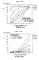
- Figs. 3(a) - (f) show the oxygen precipitation amounts for respective conditions.
- IG heat treatment conditions temperature, time
- IG heat treatment using the conditions thus determined serves to equalize the oxygen precipitation amount of the single crystal and hence improve the yield of the devices.
- the initial Oi in a silicon single crystal pulled by CZ method is approximately (16 ⁇ 0.5) x 10 17 atoms/cc and the thermal donor concentrations throughout the length of the pulled single crystal are as shown in Fig. 4.
- Table 2 shows the average values of the thermal donor concentrations for each block over the length of the single crystal. Thermal donor concentration 1.3 1.0 0.7 0.4 0.3 0.2 (x 10 15 atoms/cc)
- the optimal oxygen precipitation amount delta Oi for producing devices is more than 8 x 10 17 atoms/cc after simulation heat treatment for heat treatment A; 4 x 10 17 - 6 x 10 17 atoms/cc after simulation heat treatment for heat treatment B; and 3 x 10 17 atoms/cc or less after heat after heat treatment for heat treatment C
- the average thermal donor concentration from the top side of the single crystal to the respective blocks is as shown in Table 2. Therefore, by corresponding these values to the values in Figs. 3(a) - (f), the optimal conditions for the IG heat treatment are obtained as shown in Table 3. Temperature °C 625 625 625 625 625 625 625 Time hour 1.5 2.0 2.5 2.7 2.8 3.0
- Figs. 2(a) - (c) show the relationship between oxygen precipitation amount delta Oi and initial Oi in each of the wafers which are uniformly subjected to conventional IG heat treatment at 650° C for 2.5 hours.
- the yield of devices using wafers produced by the method of this embodiment is improved by about 10 % compared to devices using wafers produced in the conventional method.
- a so-called 2-step IG which includes outward diffusion of oxygen by a high temperature (usually higher than 1,100°C) heat treatment and subsequently a low temperature heat treatment is also applicable.
- Fig. 9 illustrates the relationship between the thermal donor concentration and oxygen precipitation amount in the case of a 2-step IG application in which a 2-step IG treatment at a higher temperature (1,175°C) and a lower temperature (700°C) is performed and then a simulation for heat treatment C is performed.
- the oxygen precipitation amount increases as the thermal donor concentration increases as in the former embodiment.
- the time for lower temperature heat treatment performed after high temperature heat treatment is required to be reduced even in the 2-step IG. It is important that the conditions of the low temperature heat treatment should be calculated according to the concentration of the thermal donors in the same manner as described above.
- the IG heat treatment is performed under the conditions determined according to the thermal donor concentration in the pulled crystal.
Landscapes
- Crystals, And After-Treatments Of Crystals (AREA)
- Liquid Deposition Of Substances Of Which Semiconductor Devices Are Composed (AREA)
Description
- The present invention relates to a heat treatment method of semiconductor wafers, particularly a wafer obtained by slicing a silicon single crystal produced by a pulling method, and more particularly to a technique for controlling the precipitation amount of oxygen in the wafer.
- In producing a silicon single crystal, for example, by a pulling method, since a crucible for containing melt of a material is usually made of quartz, oxygen of about 10 x 10 17 - 20 x 1017 atoms/cc (old ASTM) is taken into the pulled crystal. During the fabrication of a device, the oxygen taken into the crystal is supersaturated and precipitated by heat treatment, thereby to create micro defects in the crystal. Such defects caused by the precipitation of oxygen can be a gettering site of impurities. Gettering which utilizes the defects caused by oxygen precipitation is called intrinsic gettering (hereinafter referred to as IG) which is widely used as a clean gettering method. In order to fully exhibit the advantageous effect of IG, Precise control of the amount of the oxygen precipitation is required. In actuality, however, the amount of oxygen precipitation by heat treatment usually varies according to the thermal history of the crystal in the course of the pulling Process.
- The behavior of such precipitation of oxygen in a silicon wafer is described, for example, in ASTM Task Force Committee Report "Testing for Oxygen Precipitation in Silicon Wafers", Solid State Technology / March 1987, p.85.
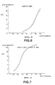
- This report shows the conditions of heat treatment for silicon wafers having various initial interstitial oxygen concentrations (hereafter referred to as initial Oi) such as 1,050 °C for 16 hours, or 750 °C for 4 hours and then 1,050 °C for 16 hours (see Table 1 for the conditions). In the report, heat treatment was performed in accordance with the heat treatment conditions of Table 1, and the difference of interstitial oxygen concentrations (hereinafter referred to as delta Oi) before the heat treatment (initial Oi) and after the heat treatment was measured. The result of the measurement is shown in Figs. 6 and 7.
1 1,050°C for 16 hrs 2 750°C for 4 hrs + 1,050°C for 16 hrs 3 800°C for 4 hrs + 1,000°C for 16 hrs 4 900°C for 4 hrs + 1,000°C for 16 hrs 5 1,000°C for 16 hrs - The heat treatment shown in Table 1 has been conventionally used as simple heat treatment conditions (hereinafter referred to as simulation heat treatment) for examining the amount of oxygen precipitation. Fig. 8 shows the yield of devices with respect to delta Oi as a result of the simulation heat treatment. To ensure that the delta Oi falls within the hatched portion of Fig. 8, that is, in the range where the yield of device is not adversely affected, a plurality of wafers having substantially the same initial Oi is subjected to IG heat treatment at 650 °C for 60 minutes as is performed conventionally. However, the delta Oi varies from wafer to wafer, and cannot always fall within the range. On average, the delta Oi draws a S-curve with respect to the initial Oi, but the variance is large.
- EP-A-0 165 364, from which the precharacterizing part of
claim 1 starts, describes a method of performing heat treatment to perform intrinsic gettering on semiconductor wafers obtained by slicing a semiconductor single crystal grown from a melt contained in a quartz crucible by a pulling method. According to EP-A-0 165 364, semiconductor wafers are sorted into different groups according to the concentration of the initial oxygen within the semiconductor wafers. For each group of semiconductors a different heat treatment temperature-time-profile is selected and the semiconductor wafers are subjected to the heat treatment according to the heat treatment temperature-time-profile selected for the respective group of semiconductor wafers. - EP-A-0 020 993 describes a method for indirectly measuring the oxygen concentration of semiconductor wafers. In this method the resistivity of a semiconductor wafer is measured prior to a heat treatment process and after the process, the change of resistivity being an indication of the amount of initial oxygen prior to the heat treatment process.
- EP-A-0 030 457 describes a method of manufacturing a semiconductor wafer in which the semiconductor wafer is treated in a two-step heat treatment process to perform an intrinsic gettering. According to EP-A-0 030 457 semiconductor wafers are annealed in a first treatment step at a temperature of 950 °C to 1 300 °C in a non-oxydising atmosphere to bring about diffusion out of oxygen near the surfaces of the semiconductor wafers. Then, the semiconductor wafers are annealed at a temperature in the range of 600 °C to 800 °C to have microdefects created in the interior of the semiconductor wafers. When the semiconductor wafers are subsequently heat-treated, microdefects of a high density capable of gettering grow in the interior of the semiconductor wafers to be microdefects of comparatively larger size. Near the surfaces, microdefects such as stacking defects are not created because the oxygen density is low.
- It is the object of the present invention to reduce variance of the delta Oi in the device manufacturing process and to generate a predetermined amount of precipitation nuclei in the semiconductor wafers with high controllability so as to improve the yield of the devices.
- This object is solved, according to the invention, with the features of
claim 1. - Some of the oxygen taken into a crystal by the pulling method becomes donors in the crystal according to the thermal history during the pulling operation. This is called thermal donors. The results of various experiments exhibit that the thermal donors facilitate the creation of oxygen precipitation defects in the crystal and that a change (delta Oi) before the IG heat treatment of the initial Oi and after the IG heat treatment greatly varies according to the thermal donor concentration in the crystal.
- The present invention has been made in view of this fact, and is characterized in that a wafer is subjected to IG heat treatment under heat treatment conditions determined according to the thermal donor concentration in the crystal directly after being pulled, thereby to cause the change (delta Oi) after the heat treatment relative to the initial Oi before thermal treatment to fall within a desired range.
- The thermal donor concentration is measured as follows.
- A thermal donor is produced when some of the oxygen taken into the crystal becomes donors according to the thermal history of the pulling process. Meanwhile, the resistivity of the crystal is determined by impurities such as phosphorus and boron which are added to the crystal beforehand. Since the resistivity of the crystal is changed according to the concentration of the thermal donors generated in the crystal, the thermal donor concentration can be determined by measuring the resistivity of the crystal. The thermal donors are eliminated by heat treatment at about 650 °C for about 30 minutes. Accordingly, the thermal donor concentration in a crystal directly after being pulled can be measured by measuring the resistivity of the crystal directly after being pulled, measuring the resistivity of the crystal after the donor eliminating process at about 650 °C for about 30 minutes and calculating the difference between the resistivities of the crystal before and after the heat treatment of the donor eliminating process. In other words, the difference between the resistivities before and after the donor elimination can be considered to correspond to the thermal donor concentration.
- In order to unify the oxygen precipitation amount, i.e., delta Oi in wafers after the device manufacturing process, the Present invention provides IG heat treatment conditions, i.e., heat treatment conditions determined according to the thermal donor concentration, which are to be employed in place of the conventional conditions so as to cause the variance of the delta Oi during the device manufacturing process to fall within a desired range with high controllability and hence improve the yield of the devices.
- Especially, for a crystal having high thermal donor concentrations in which the same temperature conditions of the IG heat treatment are used, higher controllability is achieved by performing short-time IG heat treatment on the crystal. The IG heat treatment conditions comprise temperature condition and time condition. When the temperature is changed, the delta Oi is likely to be changed due to other factors. Accordingly, control is easier by changing the time alone.
- In actual operations, wafers are prepared by slicing the respective portions having different thermal donor concentrations of a silicon single crystal manufactured by Czochralski method, and the relation between the IG heat treatment conditions (temperature and time conditions) and the oxygen precipitation amount delta Oi after simulation heat treatment is obtained. By using the relation, IG heat treatment conditions under which a target oxygen precipitation amount is given to a wafer are determined.
- In the implementation of the present invention, the resistivities, before and after the IG heat treatment, of wafers taken out from respective portions of a silicon single crystal produced by Czochralski method are converted to dopant concentrations using ASTM (F723-82), and the thermal donor concentration is calculated from the difference between these dopant concentrations. An n-type single crystal is used. Namely, thermal donor concentration = 5 x 10¹⁵ ((1/ρ1) - (1/ρ2)) where
- ρ1
- is resistivity of wafer before IG heat treatment;
- ρ2
- is resistivity of wafer after IG heat treatment.
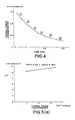
- For a wafer whose initial Oi is 15.5 x 10¹⁷ atoms/cc - 16.5 x 10¹⁷ atoms/cc, the relationship between thermal donor concentration and the oxygen precipitation amount delta Oi after each simulation heat treatment is shown in Fig. 5. It turned out that the higher the thermal donor concentration is in the single crystal when pulled, the larger the oxygen precipitation amount becomes.
- For different silicon wafers having an initial oxygen concentration of a substantially constant value of 16.0 x 10¹⁷ atoms/cc and quantity of thermal donors of 0.1 x 10¹⁵ atoms/cc - 1.6 x 10¹⁵ atoms/cc, the IG heat treatment is conducted in which temperature and time are changed between 550 and 700 °C and between 1 and 8 hours, respectively. Thereafter, the wafers are subjected to different simulation heat treatments as follows:
- (Heat treatment A)
800°C x 4 hours in N2 + 1 000°C x 16 hours in dry O2 - (Heat treatment B)
900°C x 4 hours in N2 + 1000°C x 16 hours in dry O2 - (Heat treatment C)
1,000°C x 16 hours in dry O2 -
- Figs. 3(a) - (f) show the oxygen precipitation amounts for respective conditions.
- It can be seen from Figs. 3(a) - (f) that in order to equalize the delta Oi's, the IG heat treatment time of a wafer having relatively high thermal donor concentrations is required to be reduced when the heat treatment temperature is the same . In contrast, when the heat treatment time is the same, the temperature is required to be reduced.
- Therefore, from the graphs of Figs. 3(a) - (f), IG heat treatment conditions (temperature, time) are obtained for optimizing the delta Oi for each portion of a silicon single crystal ingot whose quantity of thermal donors differs from each other. IG heat treatment using the conditions thus determined serves to equalize the oxygen precipitation amount of the single crystal and hence improve the yield of the devices. In the drawings:
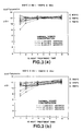
- Figs. 1(a) - (c) are graphs illustrating the relationship between the initial Oi and oxygen concentration change delta Oi before and after the heat treatment according to a method of the Present invention;
- Figs. 2(a) - (c) are graphs illustrating the relationship between the initial Oi and oxygen concentration change delta Oi before and after the heat treatment according to a conventional method;
- Figs. 3(a) - (f) are graphs illustrating the relationship between heat treatment time causing oxygen precipitation nucleus and delta Oi after simulation heat treatment;
- Fig. 4 is a graph illustrating thermal donor concentrations with respect to cure percentage of a single crystal;
- Figs. 5(a) - (c) are graphs illustrating the relationship between thermal donor concentration and change delta Oi before and after the heat treatment;
- Figs. 6 and 7 are graphs illustrating the relationship between the initial Oi and the change delta Oi before and after the heat treatment;
- Fig. 8 is a graph illustrating the relationship between the change delta Oi and device yield; and
- Fig. 9 is a graph illustrating the relationship between thermal donor concentration and the change delta Oi before and after the heat treatment.
-
- An embodiment of the present invention will be described below.
- The initial Oi in a silicon single crystal pulled by CZ method is approximately (16 ± 0.5) x 1017 atoms/cc and the thermal donor concentrations throughout the length of the pulled single crystal are as shown in Fig. 4. Table 2 shows the average values of the thermal donor concentrations for each block over the length of the single crystal.
Thermal donor concentration 1.3 1.0 0.7 0.4 0.3 0.2 (x 1015 atoms/cc) - When it is known that the optimal oxygen precipitation amount delta Oi for producing devices is more than 8 x 10¹⁷ atoms/cc after simulation heat treatment for heat treatment A; 4 x 10¹⁷ - 6
x 1017 atoms/cc after simulation heat treatment for heat treatment B; and 3 x 10¹⁷ atoms/cc or less after heat after heat treatment for heat treatment C, the average thermal donor concentration from the top side of the single crystal to the respective blocks is as shown in Table 2. Therefore, by corresponding these values to the values in Figs. 3(a) - (f), the optimal conditions for the IG heat treatment are obtained as shown in Table 3.Temperature °C 625 625 625 625 625 625 Time hour 1.5 2.0 2.5 2.7 2.8 3.0 - As a result of simulation heat treatment of the wafers cut out from the respective single crystal blocks which are subjected to IG heat treatment, the relationship between oxygen precipitation amount delta Oi and initial Oi in the wafer is as shown in Figs. 1(a) - (c).
- For comparison purposes, Figs. 2(a) - (c) show the relationship between oxygen precipitation amount delta Oi and initial Oi in each of the wafers which are uniformly subjected to conventional IG heat treatment at 650° C for 2.5 hours.
- The yield of devices using wafers produced by the method of this embodiment is improved by about 10 % compared to devices using wafers produced in the conventional method.
- As seen in this embodiment, by obtaining conditions and performing IG heat treatment according to the inventive method, the generation of varied amount of oxygen precipitation in the subsequent device manufacturing process is prevented and the yield of devices is improved.
- According to the present invention, an IG heat treatment time (t) is determined from the following recurrence formula:
- From a target oxygen precipitation amount delta Oi, the measured initial Oi and the thermal donor concentration,
- When the IG heat treatment time for 650 °C is obtained:
- While in the above embodiment an IG effect causing oxygen precipitation during a low temperature heat treatment of about 650°C is applied, a so-called 2-step IG which includes outward diffusion of oxygen by a high temperature (usually higher than 1,100°C) heat treatment and subsequently a low temperature heat treatment is also applicable.
- Fig. 9 illustrates the relationship between the thermal donor concentration and oxygen precipitation amount in the case of a 2-step IG application in which a 2-step IG treatment at a higher temperature (1,175°C) and a lower temperature (700°C) is performed and then a simulation for heat treatment C is performed. In this case, the oxygen precipitation amount increases as the thermal donor concentration increases as in the former embodiment. In order to control the oxygen Precipitation amount with high precision for a substrate having a high thermal donor concentration, the time for lower temperature heat treatment performed after high temperature heat treatment is required to be reduced even in the 2-step IG. It is important that the conditions of the low temperature heat treatment should be calculated according to the concentration of the thermal donors in the same manner as described above.
- In the present invention, the IG heat treatment is performed under the conditions determined according to the thermal donor concentration in the pulled crystal. Thus, variations in the target oxygen precipitation amount generated in the wafers in the device manufacturing process are reduced, and the yield of the devices which are end products is improved compared to the conventional uniform IG heat treatment. By doing so, efficiency of use of a single crystal ingot and hence productivity are improved.
Claims (4)
- A method of performing heat treatment on semiconductor wafers on which devices are to be fabricated, said wafers being obtained by slicing a semiconductor single crystal grown from a melt contained in a quartz crucible by a pulling method, comprising the step ofcharacterized in thatselecting a heat treatment temperature-time-profile by choosing at least one heat treatment temperature and at least one processing time and subjecting the semiconductor wafers to a heat treatment according to the selected heat treatment temperature-time-profile,the heat treatment temperature-time-profile to be selected is determined by:picking up a number of semiconductor wafers sliced from the same single crystal as the device wafers to be sample wafers,detecting the thermal donor concentration of the sample semiconductor wafers so as to detect the thermal donor concentration in respective portions of the semiconductor single crystal directly after being pulled,obtaining calibration graphs of how much oxygen precipitation occurs in each of the sample wafers after various intrinsic gettering processes wherein the time and the temperature are changed, this precipitation depending on the thermal donor concentration of the wafer and also on the pretreatment cycles used,determining the relationship between the precipitated oxygen and the initial thermal donor concentration of each of the sample wafers for each pretreatment cycle,determining the required precipitation of oxygen for the particular devices to be fabricated on the device wafers concerned,noting the thermal donor concentration in the semiconductor single crystal in the portions corresponding to where each of the device wafers originated, and then using the previously obtained calibration graphs to select the heat treatment temperature-time-profile required to generate the predetermined required amount of oxygen precipitation nuclei in each of the device wafers.
- The method of claim 1, wherein the step of calculating the thermal donor concentrations of respective portions of the pulled semiconductor single crystal is performed on the basis of a change in the resistance value of the sample wafers before and after a heat treatment which eliminates thermal donors in the semiconductor single crystal.
- The method of claim 1 or 2, characterized by the heat treatment-temperature profile comprising a high temperature heat treatment step of heating the semiconductor wafer at a constant high temperature, and a low temperature heat treatment step of performing heat treatment on the wafer at a temperature lower than the temperature in the high temperature heat treatment step.
- The method of any one of claims 1-3, wherein the calibration graphs are obtained by various different heat treatments of the sample semiconductor wafers for performing the intrinsic gettering, each heat treatment being conducted at a temperature between 550 °C and 700 °C for between one and eight hours.
Applications Claiming Priority (3)
| Application Number | Priority Date | Filing Date | Title |
|---|---|---|---|
| JP250226/90 | 1990-09-21 | ||
| JP2250226A JPH0750713B2 (en) | 1990-09-21 | 1990-09-21 | Heat treatment method for semiconductor wafers |
| PCT/JP1991/001259 WO1992005579A1 (en) | 1990-09-21 | 1991-09-20 | Semiconductor wafer heat treatment method |
Publications (3)
| Publication Number | Publication Date |
|---|---|
| EP0550750A1 EP0550750A1 (en) | 1993-07-14 |
| EP0550750A4 EP0550750A4 (en) | 1994-01-19 |
| EP0550750B1 true EP0550750B1 (en) | 1999-05-19 |
Family
ID=17204718
Family Applications (1)
| Application Number | Title | Priority Date | Filing Date |
|---|---|---|---|
| EP91916605A Expired - Lifetime EP0550750B1 (en) | 1990-09-21 | 1991-09-20 | Semiconductor wafer heat treatment method |
Country Status (5)
| Country | Link |
|---|---|
| US (1) | US5385115A (en) |
| EP (1) | EP0550750B1 (en) |
| JP (1) | JPH0750713B2 (en) |
| DE (1) | DE69131252T2 (en) |
| WO (1) | WO1992005579A1 (en) |
Families Citing this family (13)
| Publication number | Priority date | Publication date | Assignee | Title |
|---|---|---|---|---|
| JP3011982B2 (en) * | 1990-09-14 | 2000-02-21 | コマツ電子金属株式会社 | Method for manufacturing semiconductor device |
| JP2613498B2 (en) * | 1991-03-15 | 1997-05-28 | 信越半導体株式会社 | Heat treatment method for Si single crystal wafer |
| JPH0684925A (en) * | 1992-07-17 | 1994-03-25 | Toshiba Corp | Semiconductor substrate and processing method thereof |
| JP3232168B2 (en) * | 1993-07-02 | 2001-11-26 | 三菱電機株式会社 | Semiconductor substrate, method of manufacturing the same, and semiconductor device using the semiconductor substrate |
| US5593494A (en) * | 1995-03-14 | 1997-01-14 | Memc Electronic Materials, Inc. | Precision controlled precipitation of oxygen in silicon |
| KR100240023B1 (en) * | 1996-11-29 | 2000-01-15 | 윤종용 | Method of annealing semiconductor wafer and semiconductor wafer using the same |
| DE69908965T2 (en) * | 1998-10-14 | 2004-05-13 | Memc Electronic Materials, Inc. | HEAT TEMPERATURE SINGLE CRYSTAL SILICON WITH LOW ERROR DENSITY |
| TWI290182B (en) | 2004-01-27 | 2007-11-21 | Sumco Techxiv Corp | Method for predicting precipitation behavior of oxygen in silicon single crystal, determining production parameter thereof, and storage medium storing program for predicting precipitation behavior of oxygen in silicon single crystal |
| CN101228301A (en) * | 2005-05-19 | 2008-07-23 | Memc电子材料有限公司 | High resistivity silicon structure and method for making same |
| FR2964459B1 (en) * | 2010-09-02 | 2012-09-28 | Commissariat Energie Atomique | METHOD FOR MAPPING THE OXYGEN CONCENTRATION |
| US20150294868A1 (en) * | 2014-04-15 | 2015-10-15 | Infineon Technologies Ag | Method of Manufacturing Semiconductor Devices Containing Chalcogen Atoms |
| JP6716344B2 (en) * | 2016-06-01 | 2020-07-01 | グローバルウェーハズ・ジャパン株式会社 | Silicon wafer heat treatment method |
| JP6878188B2 (en) * | 2017-07-26 | 2021-05-26 | グローバルウェーハズ・ジャパン株式会社 | How to measure the resistivity of a silicon wafer |
Family Cites Families (11)
| Publication number | Priority date | Publication date | Assignee | Title |
|---|---|---|---|---|
| US4140570A (en) * | 1973-11-19 | 1979-02-20 | Texas Instruments Incorporated | Method of growing single crystal silicon by the Czochralski method which eliminates the need for post growth annealing for resistivity stabilization |
| JPS583374B2 (en) * | 1977-06-15 | 1983-01-21 | 超エル・エス・アイ技術研究組合 | Silicon single crystal processing method |
| FR2435818A1 (en) * | 1978-09-08 | 1980-04-04 | Ibm France | PROCESS FOR INCREASING THE INTERNAL TRAPPING EFFECT OF SEMICONDUCTOR BODIES |
| FR2460479A1 (en) * | 1979-06-29 | 1981-01-23 | Ibm France | PROCESS FOR CHARACTERIZING THE OXYGEN CONTENT OF SILICON BARS DRAWN ACCORDING TO THE CZOCHRALSKI METHOD |
| JPS5680139A (en) * | 1979-12-05 | 1981-07-01 | Chiyou Lsi Gijutsu Kenkyu Kumiai | Manufacture of semiconductor device |
| JPS5830137A (en) * | 1981-08-18 | 1983-02-22 | Toshiba Corp | Manufacture of wafer |
| JPS6066827A (en) * | 1983-09-24 | 1985-04-17 | Mitsubishi Metal Corp | Controlling method of introducing crystal defect into silicon wafer |
| DE3473971D1 (en) * | 1984-06-20 | 1988-10-13 | Ibm | Method of standardization and stabilization of semiconductor wafers |
| US4622082A (en) * | 1984-06-25 | 1986-11-11 | Monsanto Company | Conditioned semiconductor substrates |
| US5066599A (en) * | 1989-07-27 | 1991-11-19 | Fujitsu Limited | Silicon crystal oxygen evaluation method using fourier transform infrared spectroscopy (ftir) and semiconductor device fabrication method using the same |
| US5096839A (en) * | 1989-09-20 | 1992-03-17 | Kabushiki Kaisha Toshiba | Silicon wafer with defined interstitial oxygen concentration |
-
1990
- 1990-09-21 JP JP2250226A patent/JPH0750713B2/en not_active Expired - Lifetime
-
1991
- 1991-09-20 WO PCT/JP1991/001259 patent/WO1992005579A1/en not_active Ceased
- 1991-09-20 EP EP91916605A patent/EP0550750B1/en not_active Expired - Lifetime
- 1991-09-20 US US08/030,356 patent/US5385115A/en not_active Expired - Lifetime
- 1991-09-20 DE DE69131252T patent/DE69131252T2/en not_active Expired - Lifetime
Also Published As
| Publication number | Publication date |
|---|---|
| US5385115A (en) | 1995-01-31 |
| EP0550750A1 (en) | 1993-07-14 |
| JPH0750713B2 (en) | 1995-05-31 |
| DE69131252T2 (en) | 2000-02-24 |
| DE69131252D1 (en) | 1999-06-24 |
| EP0550750A4 (en) | 1994-01-19 |
| WO1992005579A1 (en) | 1992-04-02 |
| JPH04130732A (en) | 1992-05-01 |
Similar Documents
| Publication | Publication Date | Title |
|---|---|---|
| KR100240023B1 (en) | Method of annealing semiconductor wafer and semiconductor wafer using the same | |
| EP0503816B1 (en) | Heat treatment of Si single crystal | |
| US5611855A (en) | Method for manufacturing a calibration wafer having a microdefect-free layer of a precisely predetermined depth | |
| KR100622622B1 (en) | Method for manufacturing epitaxial silicon single crystal wafer and epitaxial silicon single crystal wafer | |
| US7521382B2 (en) | High resistivity silicon structure and a process for the preparation thereof | |
| KR100781728B1 (en) | Method for determining silicon single crystal manufacturing conditions and silicon wafer manufacturing method | |
| US5505157A (en) | Low hydrogen-content silicon crystal with few micro-defects caused from annealing, and its manufacturing methods | |
| JP2000044389A (en) | Production of epitaxial silicon single crystal wafer and epitaxial silicon single crystal wafer | |
| EP0550750A1 (en) | Semiconductor wafer heat treatment method | |
| KR100722089B1 (en) | Method for measuring point defect distribution of silicon single crystal ingot | |
| US5096839A (en) | Silicon wafer with defined interstitial oxygen concentration | |
| KR20190009354A (en) | Evaluation method and manufacturing method of silicon wafer | |
| EP0419044B1 (en) | Single crystal silicon | |
| JP4218681B2 (en) | Silicon single crystal substrate manufacturing method, resistance characteristic measuring method, and resistance characteristic guarantee method | |
| US4401506A (en) | Process for producing semiconductor device | |
| KR101001981B1 (en) | Epitaxial growth silicon wafer and epitaxial wafer and its manufacturing method | |
| EP0137209A2 (en) | Silicon wafer and its application in producing integrated circuit devices | |
| JP4302879B2 (en) | Method for producing a silicon wafer having a controlled distribution of oxygen precipitate nucleation centers | |
| Katz et al. | High oxygen Czochralski silicon crystal growth relationship to epitaxial stacking faults | |
| JP2000072595A (en) | Single silicon crystal wafer doped with boron and epitaxial silicon wafer and their production | |
| JPH04298042A (en) | Method of heat-treating semiconductor | |
| CN115280472B (en) | Method for controlling donor concentration in monocrystalline silicon substrate | |
| JP2903520B2 (en) | Evaluation method of silicon single crystal | |
| JPH0469422B2 (en) | ||
| KR101081652B1 (en) | Manufacturing Method of Silicon Wafer with Controlled Bulk Micro Defects Concentration by Low-Temperature Rapid Annealing |
Legal Events
| Date | Code | Title | Description |
|---|---|---|---|
| PUAI | Public reference made under article 153(3) epc to a published international application that has entered the european phase |
Free format text: ORIGINAL CODE: 0009012 |
|
| 17P | Request for examination filed |
Effective date: 19930317 |
|
| AK | Designated contracting states |
Kind code of ref document: A1 Designated state(s): DE GB NL |
|
| A4 | Supplementary search report drawn up and despatched |
Effective date: 19931203 |
|
| AK | Designated contracting states |
Kind code of ref document: A4 Designated state(s): DE GB NL |
|
| 17Q | First examination report despatched |
Effective date: 19950804 |
|
| GRAG | Despatch of communication of intention to grant |
Free format text: ORIGINAL CODE: EPIDOS AGRA |
|
| GRAG | Despatch of communication of intention to grant |
Free format text: ORIGINAL CODE: EPIDOS AGRA |
|
| GRAH | Despatch of communication of intention to grant a patent |
Free format text: ORIGINAL CODE: EPIDOS IGRA |
|
| GRAH | Despatch of communication of intention to grant a patent |
Free format text: ORIGINAL CODE: EPIDOS IGRA |
|
| GRAA | (expected) grant |
Free format text: ORIGINAL CODE: 0009210 |
|
| AK | Designated contracting states |
Kind code of ref document: B1 Designated state(s): DE GB NL |
|
| PG25 | Lapsed in a contracting state [announced via postgrant information from national office to epo] |
Ref country code: NL Free format text: LAPSE BECAUSE OF FAILURE TO SUBMIT A TRANSLATION OF THE DESCRIPTION OR TO PAY THE FEE WITHIN THE PRESCRIBED TIME-LIMIT Effective date: 19990519 |
|
| REF | Corresponds to: |
Ref document number: 69131252 Country of ref document: DE Date of ref document: 19990624 |
|
| PG25 | Lapsed in a contracting state [announced via postgrant information from national office to epo] |
Ref country code: GB Free format text: LAPSE BECAUSE OF NON-PAYMENT OF DUE FEES Effective date: 19990920 |
|
| PLBE | No opposition filed within time limit |
Free format text: ORIGINAL CODE: 0009261 |
|
| STAA | Information on the status of an ep patent application or granted ep patent |
Free format text: STATUS: NO OPPOSITION FILED WITHIN TIME LIMIT |
|
| 26N | No opposition filed | ||
| GBPC | Gb: european patent ceased through non-payment of renewal fee |
Effective date: 19990920 |
|
| PGFP | Annual fee paid to national office [announced via postgrant information from national office to epo] |
Ref country code: DE Payment date: 20100915 Year of fee payment: 20 |
|
| REG | Reference to a national code |
Ref country code: DE Ref legal event code: R071 Ref document number: 69131252 Country of ref document: DE |
|
| REG | Reference to a national code |
Ref country code: DE Ref legal event code: R071 Ref document number: 69131252 Country of ref document: DE |
|
| PG25 | Lapsed in a contracting state [announced via postgrant information from national office to epo] |
Ref country code: DE Free format text: LAPSE BECAUSE OF EXPIRATION OF PROTECTION Effective date: 20110921 |