EP0550021A2 - Formation auto-alignée à masque unique de CMOS-BICMOS à double-puits avec topographie à surface platte - Google Patents
Formation auto-alignée à masque unique de CMOS-BICMOS à double-puits avec topographie à surface platte Download PDFInfo
- Publication number
- EP0550021A2 EP0550021A2 EP92121935A EP92121935A EP0550021A2 EP 0550021 A2 EP0550021 A2 EP 0550021A2 EP 92121935 A EP92121935 A EP 92121935A EP 92121935 A EP92121935 A EP 92121935A EP 0550021 A2 EP0550021 A2 EP 0550021A2
- Authority
- EP
- European Patent Office
- Prior art keywords
- dielectric
- recited
- substrate
- conductivity type
- mask
- Prior art date
- Legal status (The legal status is an assumption and is not a legal conclusion. Google has not performed a legal analysis and makes no representation as to the accuracy of the status listed.)
- Withdrawn
Links
Images
Classifications
-
- H—ELECTRICITY
- H01—ELECTRIC ELEMENTS
- H01L—SEMICONDUCTOR DEVICES NOT COVERED BY CLASS H10
- H01L21/00—Processes or apparatus adapted for the manufacture or treatment of semiconductor or solid state devices or of parts thereof
- H01L21/70—Manufacture or treatment of devices consisting of a plurality of solid state components formed in or on a common substrate or of parts thereof; Manufacture of integrated circuit devices or of parts thereof
- H01L21/77—Manufacture or treatment of devices consisting of a plurality of solid state components or integrated circuits formed in, or on, a common substrate
- H01L21/78—Manufacture or treatment of devices consisting of a plurality of solid state components or integrated circuits formed in, or on, a common substrate with subsequent division of the substrate into plural individual devices
- H01L21/82—Manufacture or treatment of devices consisting of a plurality of solid state components or integrated circuits formed in, or on, a common substrate with subsequent division of the substrate into plural individual devices to produce devices, e.g. integrated circuits, each consisting of a plurality of components
- H01L21/822—Manufacture or treatment of devices consisting of a plurality of solid state components or integrated circuits formed in, or on, a common substrate with subsequent division of the substrate into plural individual devices to produce devices, e.g. integrated circuits, each consisting of a plurality of components the substrate being a semiconductor, using silicon technology
- H01L21/8232—Field-effect technology
- H01L21/8234—MIS technology, i.e. integration processes of field effect transistors of the conductor-insulator-semiconductor type
- H01L21/8238—Complementary field-effect transistors, e.g. CMOS
- H01L21/823892—Complementary field-effect transistors, e.g. CMOS with a particular manufacturing method of the wells or tubs, e.g. twin tubs, high energy well implants, buried implanted layers for lateral isolation [BILLI]
-
- H—ELECTRICITY
- H01—ELECTRIC ELEMENTS
- H01L—SEMICONDUCTOR DEVICES NOT COVERED BY CLASS H10
- H01L21/00—Processes or apparatus adapted for the manufacture or treatment of semiconductor or solid state devices or of parts thereof
- H01L21/02—Manufacture or treatment of semiconductor devices or of parts thereof
- H01L21/04—Manufacture or treatment of semiconductor devices or of parts thereof the devices having at least one potential-jump barrier or surface barrier, e.g. PN junction, depletion layer or carrier concentration layer
- H01L21/18—Manufacture or treatment of semiconductor devices or of parts thereof the devices having at least one potential-jump barrier or surface barrier, e.g. PN junction, depletion layer or carrier concentration layer the devices having semiconductor bodies comprising elements of Group IV of the Periodic System or AIIIBV compounds with or without impurities, e.g. doping materials
- H01L21/26—Bombardment with radiation
- H01L21/263—Bombardment with radiation with high-energy radiation
- H01L21/265—Bombardment with radiation with high-energy radiation producing ion implantation
- H01L21/266—Bombardment with radiation with high-energy radiation producing ion implantation using masks
-
- H—ELECTRICITY
- H01—ELECTRIC ELEMENTS
- H01L—SEMICONDUCTOR DEVICES NOT COVERED BY CLASS H10
- H01L27/00—Devices consisting of a plurality of semiconductor or other solid-state components formed in or on a common substrate
- H01L27/02—Devices consisting of a plurality of semiconductor or other solid-state components formed in or on a common substrate including semiconductor components specially adapted for rectifying, oscillating, amplifying or switching and having at least one potential-jump barrier or surface barrier; including integrated passive circuit elements with at least one potential-jump barrier or surface barrier
- H01L27/04—Devices consisting of a plurality of semiconductor or other solid-state components formed in or on a common substrate including semiconductor components specially adapted for rectifying, oscillating, amplifying or switching and having at least one potential-jump barrier or surface barrier; including integrated passive circuit elements with at least one potential-jump barrier or surface barrier the substrate being a semiconductor body
- H01L27/06—Devices consisting of a plurality of semiconductor or other solid-state components formed in or on a common substrate including semiconductor components specially adapted for rectifying, oscillating, amplifying or switching and having at least one potential-jump barrier or surface barrier; including integrated passive circuit elements with at least one potential-jump barrier or surface barrier the substrate being a semiconductor body including a plurality of individual components in a non-repetitive configuration
- H01L27/0611—Devices consisting of a plurality of semiconductor or other solid-state components formed in or on a common substrate including semiconductor components specially adapted for rectifying, oscillating, amplifying or switching and having at least one potential-jump barrier or surface barrier; including integrated passive circuit elements with at least one potential-jump barrier or surface barrier the substrate being a semiconductor body including a plurality of individual components in a non-repetitive configuration integrated circuits having a two-dimensional layout of components without a common active region
- H01L27/0617—Devices consisting of a plurality of semiconductor or other solid-state components formed in or on a common substrate including semiconductor components specially adapted for rectifying, oscillating, amplifying or switching and having at least one potential-jump barrier or surface barrier; including integrated passive circuit elements with at least one potential-jump barrier or surface barrier the substrate being a semiconductor body including a plurality of individual components in a non-repetitive configuration integrated circuits having a two-dimensional layout of components without a common active region comprising components of the field-effect type
- H01L27/0623—Devices consisting of a plurality of semiconductor or other solid-state components formed in or on a common substrate including semiconductor components specially adapted for rectifying, oscillating, amplifying or switching and having at least one potential-jump barrier or surface barrier; including integrated passive circuit elements with at least one potential-jump barrier or surface barrier the substrate being a semiconductor body including a plurality of individual components in a non-repetitive configuration integrated circuits having a two-dimensional layout of components without a common active region comprising components of the field-effect type in combination with bipolar transistors
-
- H—ELECTRICITY
- H01—ELECTRIC ELEMENTS
- H01L—SEMICONDUCTOR DEVICES NOT COVERED BY CLASS H10
- H01L27/00—Devices consisting of a plurality of semiconductor or other solid-state components formed in or on a common substrate
- H01L27/02—Devices consisting of a plurality of semiconductor or other solid-state components formed in or on a common substrate including semiconductor components specially adapted for rectifying, oscillating, amplifying or switching and having at least one potential-jump barrier or surface barrier; including integrated passive circuit elements with at least one potential-jump barrier or surface barrier
- H01L27/04—Devices consisting of a plurality of semiconductor or other solid-state components formed in or on a common substrate including semiconductor components specially adapted for rectifying, oscillating, amplifying or switching and having at least one potential-jump barrier or surface barrier; including integrated passive circuit elements with at least one potential-jump barrier or surface barrier the substrate being a semiconductor body
- H01L27/08—Devices consisting of a plurality of semiconductor or other solid-state components formed in or on a common substrate including semiconductor components specially adapted for rectifying, oscillating, amplifying or switching and having at least one potential-jump barrier or surface barrier; including integrated passive circuit elements with at least one potential-jump barrier or surface barrier the substrate being a semiconductor body including only semiconductor components of a single kind
- H01L27/085—Devices consisting of a plurality of semiconductor or other solid-state components formed in or on a common substrate including semiconductor components specially adapted for rectifying, oscillating, amplifying or switching and having at least one potential-jump barrier or surface barrier; including integrated passive circuit elements with at least one potential-jump barrier or surface barrier the substrate being a semiconductor body including only semiconductor components of a single kind including field-effect components only
- H01L27/088—Devices consisting of a plurality of semiconductor or other solid-state components formed in or on a common substrate including semiconductor components specially adapted for rectifying, oscillating, amplifying or switching and having at least one potential-jump barrier or surface barrier; including integrated passive circuit elements with at least one potential-jump barrier or surface barrier the substrate being a semiconductor body including only semiconductor components of a single kind including field-effect components only the components being field-effect transistors with insulated gate
- H01L27/092—Devices consisting of a plurality of semiconductor or other solid-state components formed in or on a common substrate including semiconductor components specially adapted for rectifying, oscillating, amplifying or switching and having at least one potential-jump barrier or surface barrier; including integrated passive circuit elements with at least one potential-jump barrier or surface barrier the substrate being a semiconductor body including only semiconductor components of a single kind including field-effect components only the components being field-effect transistors with insulated gate complementary MIS field-effect transistors
- H01L27/0928—Devices consisting of a plurality of semiconductor or other solid-state components formed in or on a common substrate including semiconductor components specially adapted for rectifying, oscillating, amplifying or switching and having at least one potential-jump barrier or surface barrier; including integrated passive circuit elements with at least one potential-jump barrier or surface barrier the substrate being a semiconductor body including only semiconductor components of a single kind including field-effect components only the components being field-effect transistors with insulated gate complementary MIS field-effect transistors comprising both N- and P- wells in the substrate, e.g. twin-tub
Definitions
- CMOS and BiCMOS technologies employ twin (n and p) wells in order to allow simultaneous optimization of the NMOS and PMOS transistors.
- the conventional twin well formation processes employ one or two microlithography masking steps.
- the two-mask fabrication process has the advantage that it does not degrade the silicon surface planarity or topography. This is an important requirement in advanced sub-0.5 ⁇ m CMOS and BiCMOS technologies where even a small (e.g. a few thousand ⁇ ) step between the n-well and p-well regions can result in gate length variations between the NMOS and PMOS transistors (due to the limited depth-of-focus orDOF budget in advanced photo-lithography tools).
- CMOS transistor gate length variations can degrade manufacturability and yield.
- the process simplicity of the conventional one-mask fabrication process is not a strong and sufficient advantage/improvement to justify its use in sub-0.5 ⁇ m semiconductor technologies since the one-mask process consumes silicon when masking a particular area to provide a well region.
- Such oxidation-induced silicon consumption results in uneven planarity of the PMOS and NMOS gates as shall be explained below.
- the potential gate length variability caused by the nonplanar n and p well surfaces ad DOF limitation imposes the above-mentioned obstacle.
- the surface topography problem in the conventional one-mask fabrication process is generated by a selective thermal oxidation process.
- An oxide/nitride stack is patterned and is used (usually along with the photoresist mask) as an ion implantation mask to define one of the wells.
- an oxidation step is performed which selectively defines an oxide hard mask over the implanted region.
- a second ion implantation step is used to define the second (opposite) well regions.
- a surface topography or step is produced between the n and p well regions due to the silicon consumption by the selective thermal oxidation step.
- CMOS and BiCMOS technologies usually rely on a two-mask (non-self aligned) process to define the n-well and p-well regions.
- patterned photoresist (or hard mask) layers are used as ion implantation masks. No surface step or topography is produced, therefore allowing uniform PMOS and NMOS gate patterning.
- the use of one additional masking process adds to the overall process cost and complexity.
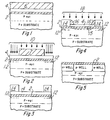
- Figures 1 through 5 illustrate cross-sectional drawings of the resulting structure from the following processing steps.
- a single-mask self-aligned process is disclosed for formation of n and p wells for advanced CMOS and BiCMOS technologies.
- the proposed process forms n-well and p-well regions using a single microlithography masking step along with a selective semiconductor (Si or GeSi) growth (SSG) process without producing surface topography or degrading surface planarity.
- Si or GeSi selective semiconductor growth
- This simple process ensures uniform NMOS and PMOS gate patterning due to fat surface topography.
- the n-to-p well placement is self-aligned due to the use of a disposable SSG hard mask.
- the invention provides a single-mask self-aligned twin well formation process for advanced CMOS and BiCMOS technologies.
- the process is based on the use of a selectively grown semiconductor (or metal) hard mask.
- the process flow for the preferred embodiment of the process flow is as follows:
Applications Claiming Priority (2)
| Application Number | Priority Date | Filing Date | Title |
|---|---|---|---|
| US814547 | 1991-12-30 | ||
| US07/814,547 US5252501A (en) | 1991-12-30 | 1991-12-30 | Self-aligned single-mask CMOS/BiCMOS twin-well formation with flat surface topography |
Publications (2)
| Publication Number | Publication Date |
|---|---|
| EP0550021A2 true EP0550021A2 (fr) | 1993-07-07 |
| EP0550021A3 EP0550021A3 (en) | 1996-12-27 |
Family
ID=25215385
Family Applications (1)
| Application Number | Title | Priority Date | Filing Date |
|---|---|---|---|
| EP92121935A Withdrawn EP0550021A3 (en) | 1991-12-30 | 1992-12-23 | Self-aligned single-mask cmos/bicmos twin-well formation with flat surface topography |
Country Status (4)
| Country | Link |
|---|---|
| US (1) | US5252501A (fr) |
| EP (1) | EP0550021A3 (fr) |
| JP (1) | JPH06112420A (fr) |
| TW (1) | TW217461B (fr) |
Cited By (3)
| Publication number | Priority date | Publication date | Assignee | Title |
|---|---|---|---|---|
| EP0696062A3 (fr) * | 1994-07-28 | 1996-12-11 | Hitachi Ltd | Dispositif semi-conducteur CMOS et procédé de fabrication associé |
| DE19603794A1 (de) * | 1995-07-26 | 1997-01-30 | Lg Semicon Co Ltd | Verfahren zum Ausbilden einer Doppelsenke für Halbleiteranordnungen |
| WO2007010732A1 (fr) * | 2005-07-19 | 2007-01-25 | Nissan Motor Co., Ltd. | Procédé de fabrication de dispositif à semi-conducteurs |
Families Citing this family (13)
| Publication number | Priority date | Publication date | Assignee | Title |
|---|---|---|---|---|
| US5583062A (en) * | 1995-06-07 | 1996-12-10 | Lsi Logic Corporation | Self-aligned twin well process having a SiO2 -polysilicon-SiO2 barrier mask |
| US5763302A (en) * | 1995-06-07 | 1998-06-09 | Lsi Logic Corporation | Self-aligned twin well process |
| US5770492A (en) * | 1995-06-07 | 1998-06-23 | Lsi Logic Corporation | Self-aligned twin well process |
| US5670393A (en) * | 1995-07-12 | 1997-09-23 | Lsi Logic Corporation | Method of making combined metal oxide semiconductor and junction field effect transistor device |
| US5547894A (en) * | 1995-12-21 | 1996-08-20 | International Business Machines Corporation | CMOS processing with low and high-current FETs |
| US5670395A (en) * | 1996-04-29 | 1997-09-23 | Chartered Semiconductor Manufacturing Pte. Ltd. | Process for self-aligned twin wells without N-well and P-well height difference |
| DE59813593D1 (de) * | 1997-04-29 | 2006-07-27 | Infineon Technologies Ag | Verfahren zur Herstellung einer CMOS-Schaltungsanordnung |
| US5956583A (en) * | 1997-06-30 | 1999-09-21 | Fuller; Robert T. | Method for forming complementary wells and self-aligned trench with a single mask |
| US6307230B1 (en) * | 1999-01-05 | 2001-10-23 | Texas Instruments Incorporated | Transistor having an improved sidewall gate structure and method of construction |
| US6235568B1 (en) * | 1999-01-22 | 2001-05-22 | Intel Corporation | Semiconductor device having deposited silicon regions and a method of fabrication |
| US6207538B1 (en) | 1999-12-28 | 2001-03-27 | Taiwan Semiconductor Manufacturing Company | Method for forming n and p wells in a semiconductor substrate using a single masking step |
| DE10052680C2 (de) * | 2000-10-24 | 2002-10-24 | Advanced Micro Devices Inc | Verfahren zum Einstellen einer Form einer auf einem Substrat gebildeten Oxidschicht |
| US6586296B1 (en) * | 2001-04-30 | 2003-07-01 | Cypress Semiconductor Corp. | Method of doping wells, channels, and gates of dual gate CMOS technology with reduced number of masks |
Citations (3)
| Publication number | Priority date | Publication date | Assignee | Title |
|---|---|---|---|---|
| US4558508A (en) * | 1984-10-15 | 1985-12-17 | International Business Machines Corporation | Process of making dual well CMOS semiconductor structure with aligned field-dopings using single masking step |
| EP0320977A2 (fr) * | 1987-12-18 | 1989-06-21 | Kabushiki Kaisha Toshiba | Procédé pour fabriquer des dispositifs semi-conducteurs comportant des puits jumeaux |
| US5070029A (en) * | 1989-10-30 | 1991-12-03 | Motorola, Inc. | Semiconductor process using selective deposition |
Family Cites Families (4)
| Publication number | Priority date | Publication date | Assignee | Title |
|---|---|---|---|---|
| US4050965A (en) * | 1975-10-21 | 1977-09-27 | The United States Of America As Represented By The Secretary Of The Air Force | Simultaneous fabrication of CMOS transistors and bipolar devices |
| US4424621A (en) * | 1981-12-30 | 1984-01-10 | International Business Machines Corporation | Method to fabricate stud structure for self-aligned metallization |
| US4527325A (en) * | 1983-12-23 | 1985-07-09 | International Business Machines Corporation | Process for fabricating semiconductor devices utilizing a protective film during high temperature annealing |
| US5132241A (en) * | 1991-04-15 | 1992-07-21 | Industrial Technology Research Institute | Method of manufacturing minimum counterdoping in twin well process |
-
1991
- 1991-12-30 US US07/814,547 patent/US5252501A/en not_active Expired - Lifetime
-
1992
- 1992-12-23 EP EP92121935A patent/EP0550021A3/en not_active Withdrawn
-
1993
- 1993-01-04 JP JP5029576A patent/JPH06112420A/ja active Pending
- 1993-04-22 TW TW082103072A patent/TW217461B/zh active
Patent Citations (3)
| Publication number | Priority date | Publication date | Assignee | Title |
|---|---|---|---|---|
| US4558508A (en) * | 1984-10-15 | 1985-12-17 | International Business Machines Corporation | Process of making dual well CMOS semiconductor structure with aligned field-dopings using single masking step |
| EP0320977A2 (fr) * | 1987-12-18 | 1989-06-21 | Kabushiki Kaisha Toshiba | Procédé pour fabriquer des dispositifs semi-conducteurs comportant des puits jumeaux |
| US5070029A (en) * | 1989-10-30 | 1991-12-03 | Motorola, Inc. | Semiconductor process using selective deposition |
Non-Patent Citations (3)
| Title |
|---|
| IEEE ELECTRON DEVICE LETTERS, vol. 9, no. 4, April 1988, NEW YORK US, pages 189-192, XP000133359 J.R. PFIESTER: "LDD MOSFET's using disposable sidewall spacer technology" * |
| INTERNATIONAL ELECTRON DEVICES MEETING TECHNICAL DIGEST, 3 - 6 December 1989, WASHINGTON, D.C., USA, pages 769-772, XP000448305 J.R. PFIESTER ET AL.: "A self-aligned LDD/channel implanted ITLDD process with selectively-deposited poly gates for CMOS VLSI" * |
| INTERNATIONAL ELECTRON DEVICES MEETING TECHNICAL DIGEST, 8 - 11 December 1991, WASHINGTON D.C., USA, pages 637-640, XP000342205 K. KANBA ET AL.: "A 7 mask CMOS technology utilizing liquid phase selective oxide deposition" * |
Cited By (8)
| Publication number | Priority date | Publication date | Assignee | Title |
|---|---|---|---|---|
| EP0696062A3 (fr) * | 1994-07-28 | 1996-12-11 | Hitachi Ltd | Dispositif semi-conducteur CMOS et procédé de fabrication associé |
| US6368905B1 (en) | 1994-07-28 | 2002-04-09 | Hitachi, Ltd. | Process for manufacturing a semiconductor wafer, a semiconductor wafer, process for manufacturing a semiconductor integrated circuit device, and semiconductor integrated circuit device |
| US6630375B2 (en) | 1994-07-28 | 2003-10-07 | Hitachi, Ltd. | Process for manufacturing a semiconductor wafer, a semiconductor wafer, process for manufacturing a semiconductor integrated circuit device, and semiconductor integrated circuit device |
| US6806130B2 (en) | 1994-07-28 | 2004-10-19 | Renesas Technology Corp. | Process for manufacturing a semiconductor wafer, a semiconductor wafer, process for manufacturing a semiconductor integrated circuit device, and semiconductor integrated circuit device |
| DE19603794A1 (de) * | 1995-07-26 | 1997-01-30 | Lg Semicon Co Ltd | Verfahren zum Ausbilden einer Doppelsenke für Halbleiteranordnungen |
| DE19603794B4 (de) * | 1995-07-26 | 2004-06-03 | LG Semicon Co., Ltd., Cheongju | Verfahren zum Ausbilden einer Doppelwanne für Halbleiteranordnungen |
| WO2007010732A1 (fr) * | 2005-07-19 | 2007-01-25 | Nissan Motor Co., Ltd. | Procédé de fabrication de dispositif à semi-conducteurs |
| US7749845B2 (en) | 2005-07-19 | 2010-07-06 | Nissan Motor Co., Ltd. | Semiconductor device manufacturing method |
Also Published As
| Publication number | Publication date |
|---|---|
| JPH06112420A (ja) | 1994-04-22 |
| EP0550021A3 (en) | 1996-12-27 |
| US5252501A (en) | 1993-10-12 |
| TW217461B (fr) | 1993-12-11 |
Similar Documents
| Publication | Publication Date | Title |
|---|---|---|
| US5252501A (en) | Self-aligned single-mask CMOS/BiCMOS twin-well formation with flat surface topography | |
| US5573963A (en) | Method of forming self-aligned twin tub CMOS devices | |
| US6930030B2 (en) | Method of forming an electronic device on a recess in the surface of a thin film of silicon etched to a precise thickness | |
| US6294416B1 (en) | Method of fabricating CMOS transistors with self-aligned planarization twin-well by using fewer mask counts | |
| US20040014292A1 (en) | Sub-micron MOS transistor | |
| US5654213A (en) | Method for fabricating a CMOS device | |
| JP4751004B2 (ja) | 厚さが異なる領域を有するデバイスまたはデバイス層の製造方法 | |
| US5654212A (en) | Method for making a variable length LDD spacer structure | |
| US6821836B2 (en) | Disposable spacer | |
| KR100507856B1 (ko) | Mos트랜지스터 제조방법 | |
| JPH02162761A (ja) | Mosfetの製造方法 | |
| US5976952A (en) | Implanted isolation structure formation for high density CMOS integrated circuits | |
| US5612242A (en) | Trench isolation method for CMOS transistor | |
| US5696016A (en) | Process for manufacturing a CMOSFET intergrated circuit | |
| EP0561167A2 (fr) | Méthode et structure d'un petit semi-conducteur | |
| US5714398A (en) | Self-aligned tungsten strapped source/drain and gate technology for deep submicron CMOS | |
| US6365468B1 (en) | Method for forming doped p-type gate with anti-reflection layer | |
| JPH05267331A (ja) | Mos型半導体装置の製造方法 | |
| US6251744B1 (en) | Implant method to improve characteristics of high voltage isolation and high voltage breakdown | |
| US6110788A (en) | Surface channel MOS transistors, methods for making the same, and semiconductor devices containing the same | |
| US6284578B1 (en) | MOS transistors having dual gates and self-aligned interconnect contact windows | |
| US6376293B1 (en) | Shallow drain extenders for CMOS transistors using replacement gate design | |
| US6162714A (en) | Method of forming thin polygates for sub quarter micron CMOS process | |
| EP0434182B1 (fr) | Procédé de fabrication de couches enterrées pour circuits intégrés | |
| US5946579A (en) | Stacked mask integration technique for advanced CMOS transistor formation |
Legal Events
| Date | Code | Title | Description |
|---|---|---|---|
| PUAI | Public reference made under article 153(3) epc to a published international application that has entered the european phase |
Free format text: ORIGINAL CODE: 0009012 |
|
| AK | Designated contracting states |
Kind code of ref document: A2 Designated state(s): DE FR GB IT NL |
|
| PUAL | Search report despatched |
Free format text: ORIGINAL CODE: 0009013 |
|
| AK | Designated contracting states |
Kind code of ref document: A3 Designated state(s): DE FR GB IT NL |
|
| 17P | Request for examination filed |
Effective date: 19970624 |
|
| 17Q | First examination report despatched |
Effective date: 20040824 |
|
| STAA | Information on the status of an ep patent application or granted ep patent |
Free format text: STATUS: THE APPLICATION IS DEEMED TO BE WITHDRAWN |
|
| 18D | Application deemed to be withdrawn |
Effective date: 20050105 |