EP0549993B1 - Stereolithographic apparatus and method of forming a model - Google Patents
Stereolithographic apparatus and method of forming a model Download PDFInfo
- Publication number
- EP0549993B1 EP0549993B1 EP92121770A EP92121770A EP0549993B1 EP 0549993 B1 EP0549993 B1 EP 0549993B1 EP 92121770 A EP92121770 A EP 92121770A EP 92121770 A EP92121770 A EP 92121770A EP 0549993 B1 EP0549993 B1 EP 0549993B1
- Authority
- EP
- European Patent Office
- Prior art keywords
- liquid
- stereolithographic
- resin
- radiation
- stereolithographic apparatus
- Prior art date
- Legal status (The legal status is an assumption and is not a legal conclusion. Google has not performed a legal analysis and makes no representation as to the accuracy of the status listed.)
- Expired - Lifetime
Links
- 238000000034 method Methods 0.000 title claims description 24
- 239000007788 liquid Substances 0.000 claims description 49
- 229920005989 resin Polymers 0.000 claims description 23
- 239000011347 resin Substances 0.000 claims description 23
- 230000005855 radiation Effects 0.000 claims description 13
- 238000005286 illumination Methods 0.000 claims description 12
- 239000010408 film Substances 0.000 claims description 11
- 229920000642 polymer Polymers 0.000 claims description 7
- 239000010409 thin film Substances 0.000 claims description 5
- 230000003028 elevating effect Effects 0.000 claims description 2
- 230000007246 mechanism Effects 0.000 claims description 2
- 239000000906 photoactive agent Substances 0.000 claims 2
- 238000001723 curing Methods 0.000 claims 1
- 238000003847 radiation curing Methods 0.000 claims 1
- 230000008569 process Effects 0.000 description 14
- 239000004033 plastic Substances 0.000 description 8
- 229920003023 plastic Polymers 0.000 description 8
- 230000008901 benefit Effects 0.000 description 6
- 238000004519 manufacturing process Methods 0.000 description 6
- 239000000203 mixture Substances 0.000 description 5
- 230000003287 optical effect Effects 0.000 description 4
- 230000037361 pathway Effects 0.000 description 4
- 241000761557 Lamina Species 0.000 description 3
- 239000011159 matrix material Substances 0.000 description 3
- HEFNNWSXXWATRW-UHFFFAOYSA-N Ibuprofen Chemical compound CC(C)CC1=CC=C(C(C)C(O)=O)C=C1 HEFNNWSXXWATRW-UHFFFAOYSA-N 0.000 description 2
- 238000011960 computer-aided design Methods 0.000 description 2
- 238000013461 design Methods 0.000 description 2
- 230000005670 electromagnetic radiation Effects 0.000 description 2
- 238000005516 engineering process Methods 0.000 description 2
- 239000007787 solid Substances 0.000 description 2
- 241000220010 Rhode Species 0.000 description 1
- XUIMIQQOPSSXEZ-UHFFFAOYSA-N Silicon Chemical compound [Si] XUIMIQQOPSSXEZ-UHFFFAOYSA-N 0.000 description 1
- 230000008859 change Effects 0.000 description 1
- 238000006243 chemical reaction Methods 0.000 description 1
- 239000011248 coating agent Substances 0.000 description 1
- 238000000576 coating method Methods 0.000 description 1
- 230000001419 dependent effect Effects 0.000 description 1
- 239000010432 diamond Substances 0.000 description 1
- 238000011156 evaluation Methods 0.000 description 1
- 229910052736 halogen Inorganic materials 0.000 description 1
- 238000003384 imaging method Methods 0.000 description 1
- 239000011344 liquid material Substances 0.000 description 1
- 239000011342 resin composition Substances 0.000 description 1
- 230000000284 resting effect Effects 0.000 description 1
- 229910052710 silicon Inorganic materials 0.000 description 1
- 239000010703 silicon Substances 0.000 description 1
- 239000007921 spray Substances 0.000 description 1
- 238000006467 substitution reaction Methods 0.000 description 1
- 238000012360 testing method Methods 0.000 description 1
- 230000009466 transformation Effects 0.000 description 1
- 230000000007 visual effect Effects 0.000 description 1
- 235000012431 wafers Nutrition 0.000 description 1
Images

Classifications
-
- G—PHYSICS
- G03—PHOTOGRAPHY; CINEMATOGRAPHY; ANALOGOUS TECHNIQUES USING WAVES OTHER THAN OPTICAL WAVES; ELECTROGRAPHY; HOLOGRAPHY
- G03F—PHOTOMECHANICAL PRODUCTION OF TEXTURED OR PATTERNED SURFACES, e.g. FOR PRINTING, FOR PROCESSING OF SEMICONDUCTOR DEVICES; MATERIALS THEREFOR; ORIGINALS THEREFOR; APPARATUS SPECIALLY ADAPTED THEREFOR
- G03F7/00—Photomechanical, e.g. photolithographic, production of textured or patterned surfaces, e.g. printing surfaces; Materials therefor, e.g. comprising photoresists; Apparatus specially adapted therefor
- G03F7/70—Microphotolithographic exposure; Apparatus therefor
- G03F7/70416—2.5D lithography
-
- B—PERFORMING OPERATIONS; TRANSPORTING
- B29—WORKING OF PLASTICS; WORKING OF SUBSTANCES IN A PLASTIC STATE IN GENERAL
- B29C—SHAPING OR JOINING OF PLASTICS; SHAPING OF MATERIAL IN A PLASTIC STATE, NOT OTHERWISE PROVIDED FOR; AFTER-TREATMENT OF THE SHAPED PRODUCTS, e.g. REPAIRING
- B29C64/00—Additive manufacturing, i.e. manufacturing of three-dimensional [3D] objects by additive deposition, additive agglomeration or additive layering, e.g. by 3D printing, stereolithography or selective laser sintering
- B29C64/10—Processes of additive manufacturing
- B29C64/106—Processes of additive manufacturing using only liquids or viscous materials, e.g. depositing a continuous bead of viscous material
- B29C64/124—Processes of additive manufacturing using only liquids or viscous materials, e.g. depositing a continuous bead of viscous material using layers of liquid which are selectively solidified
- B29C64/129—Processes of additive manufacturing using only liquids or viscous materials, e.g. depositing a continuous bead of viscous material using layers of liquid which are selectively solidified characterised by the energy source therefor, e.g. by global irradiation combined with a mask
-
- B—PERFORMING OPERATIONS; TRANSPORTING
- B33—ADDITIVE MANUFACTURING TECHNOLOGY
- B33Y—ADDITIVE MANUFACTURING, i.e. MANUFACTURING OF THREE-DIMENSIONAL [3-D] OBJECTS BY ADDITIVE DEPOSITION, ADDITIVE AGGLOMERATION OR ADDITIVE LAYERING, e.g. BY 3-D PRINTING, STEREOLITHOGRAPHY OR SELECTIVE LASER SINTERING
- B33Y10/00—Processes of additive manufacturing
-
- B—PERFORMING OPERATIONS; TRANSPORTING
- B33—ADDITIVE MANUFACTURING TECHNOLOGY
- B33Y—ADDITIVE MANUFACTURING, i.e. MANUFACTURING OF THREE-DIMENSIONAL [3-D] OBJECTS BY ADDITIVE DEPOSITION, ADDITIVE AGGLOMERATION OR ADDITIVE LAYERING, e.g. BY 3-D PRINTING, STEREOLITHOGRAPHY OR SELECTIVE LASER SINTERING
- B33Y30/00—Apparatus for additive manufacturing; Details thereof or accessories therefor
-
- G—PHYSICS
- G02—OPTICS
- G02B—OPTICAL ELEMENTS, SYSTEMS OR APPARATUS
- G02B26/00—Optical devices or arrangements for the control of light using movable or deformable optical elements
- G02B26/08—Optical devices or arrangements for the control of light using movable or deformable optical elements for controlling the direction of light
- G02B26/0816—Optical devices or arrangements for the control of light using movable or deformable optical elements for controlling the direction of light by means of one or more reflecting elements
- G02B26/0833—Optical devices or arrangements for the control of light using movable or deformable optical elements for controlling the direction of light by means of one or more reflecting elements the reflecting element being a micromechanical device, e.g. a MEMS mirror, DMD
- G02B26/0841—Optical devices or arrangements for the control of light using movable or deformable optical elements for controlling the direction of light by means of one or more reflecting elements the reflecting element being a micromechanical device, e.g. a MEMS mirror, DMD the reflecting element being moved or deformed by electrostatic means
-
- G—PHYSICS
- G03—PHOTOGRAPHY; CINEMATOGRAPHY; ANALOGOUS TECHNIQUES USING WAVES OTHER THAN OPTICAL WAVES; ELECTROGRAPHY; HOLOGRAPHY
- G03F—PHOTOMECHANICAL PRODUCTION OF TEXTURED OR PATTERNED SURFACES, e.g. FOR PRINTING, FOR PROCESSING OF SEMICONDUCTOR DEVICES; MATERIALS THEREFOR; ORIGINALS THEREFOR; APPARATUS SPECIALLY ADAPTED THEREFOR
- G03F7/00—Photomechanical, e.g. photolithographic, production of textured or patterned surfaces, e.g. printing surfaces; Materials therefor, e.g. comprising photoresists; Apparatus specially adapted therefor
- G03F7/0037—Production of three-dimensional images
-
- G—PHYSICS
- G03—PHOTOGRAPHY; CINEMATOGRAPHY; ANALOGOUS TECHNIQUES USING WAVES OTHER THAN OPTICAL WAVES; ELECTROGRAPHY; HOLOGRAPHY
- G03F—PHOTOMECHANICAL PRODUCTION OF TEXTURED OR PATTERNED SURFACES, e.g. FOR PRINTING, FOR PROCESSING OF SEMICONDUCTOR DEVICES; MATERIALS THEREFOR; ORIGINALS THEREFOR; APPARATUS SPECIALLY ADAPTED THEREFOR
- G03F7/00—Photomechanical, e.g. photolithographic, production of textured or patterned surfaces, e.g. printing surfaces; Materials therefor, e.g. comprising photoresists; Apparatus specially adapted therefor
- G03F7/20—Exposure; Apparatus therefor
- G03F7/2002—Exposure; Apparatus therefor with visible light or UV light, through an original having an opaque pattern on a transparent support, e.g. film printing, projection printing; by reflection of visible or UV light from an original such as a printed image
- G03F7/2012—Exposure; Apparatus therefor with visible light or UV light, through an original having an opaque pattern on a transparent support, e.g. film printing, projection printing; by reflection of visible or UV light from an original such as a printed image using liquid photohardening compositions, e.g. for the production of reliefs such as flexographic plates or stamps
-
- B—PERFORMING OPERATIONS; TRANSPORTING
- B29—WORKING OF PLASTICS; WORKING OF SUBSTANCES IN A PLASTIC STATE IN GENERAL
- B29C—SHAPING OR JOINING OF PLASTICS; SHAPING OF MATERIAL IN A PLASTIC STATE, NOT OTHERWISE PROVIDED FOR; AFTER-TREATMENT OF THE SHAPED PRODUCTS, e.g. REPAIRING
- B29C35/00—Heating, cooling or curing, e.g. crosslinking or vulcanising; Apparatus therefor
- B29C35/02—Heating or curing, e.g. crosslinking or vulcanizing during moulding, e.g. in a mould
- B29C35/08—Heating or curing, e.g. crosslinking or vulcanizing during moulding, e.g. in a mould by wave energy or particle radiation
- B29C35/0805—Heating or curing, e.g. crosslinking or vulcanizing during moulding, e.g. in a mould by wave energy or particle radiation using electromagnetic radiation
- B29C2035/0838—Heating or curing, e.g. crosslinking or vulcanizing during moulding, e.g. in a mould by wave energy or particle radiation using electromagnetic radiation using laser
Definitions
- This invention relates to a stereolithographic apparatus as defined in the precharacterizing part of claim 1 and to a method as defined in the precharacterizing part of claim 9.
- a stereolithographic apparatus and a method as mentioned above are known from WO-A-91/12120.
- This document describes a method and apparatus for forming a solid three-dimensional article by exposure of successive layers of a liquid material to a vertically movable energy source.
- the apparatus includes a fixed support plate disposed in a container, the liquid being dispensed to successively higher levels in the container above the plate.
- the liquid is fed from a reservoir below the plate to an upper portion of the container above the plate by an expandable member disposed in the reservoir.
- a vertically movable liquid dispenser may be provided above the plate either alone or in combination with the expandable member.
- the energy source includes a laser, a focusing optics system and a scanner head for directing a laser beam to solidify selected portions of successive layers of the liquid medium.
- Stereolithography is a process by which three dimensional objects are fabricated from thin layers of hardened or cured liquid polymers.
- the liquid polymers or resins are selectively hardened by an intense light source of suitable wave length.
- an ultraviolet (“UV"), argon-ion, or other type of laser is used to harden the liquid polymer.
- UV ultraviolet
- argon-ion or other type of laser
- the particular laser is directed to a thin film of the polymer by an x-y scanner interpreting, typically, computer-aided design (“CAD”) data.
- CAD data mathematically represents the shape of the object to be produced as a series of sequential thin layers of laminas, typically 1/100th of an inch in thickness.
- the object may thereby be produced by curing portions of a film of resin that correspond to the first layer of the object, by coating the hardened layer with a uniform thin liquid film, and by curing portions of the second film that correspond to the next lamina of the object. This process is repeated until each lamina of the model has been reproduced as a layer of hardened polymer.
- the model produced by stereolithography may be used for testing and evaluation of engineering designs, for tooling purposes and for low volume manufacturing applications.
- Known stereolithographic process devices and methods are limited by at least two characteristics.
- each resin may be hardened by only one type of laser. This results in little or no ability to change the resin composition without expensive hardware changes. Also, not all wavelengths of radiation may be produced as laser light. This precludes the use of certain resins because no laser exists to cure them.
- EP-A-0 450 762 a solid imaging apparatus and method is described which produces an integral three-dimensional object from a multiplicity of cross sectional portions of the object by selectively exposing successive layers of a liquid photoformable composition to actinic radiation.
- the apparatus includes a vessel for containing the composition so as to present a free surface, and a movable platform disposed within the vessel below the free surface. Part of the composition is transferred above the free surface, by lowering and raising a dispenser at predetermined positions located away from the platform. A doctor blade contacts the composition transferred above the free surface and then moves over the platform to form a substantially uniform layer of the composition.
- Document EP-A-0 391 529 describes a visual display system having a spatial light modulator with individually and simultaneously controllable elements. Each element capable of producing an individual light beam directed toward a display surface. A source of random polarity light is utilized to direct light onto the modulator.
- Document WO-A-89/09687 relates to a system for producing precision plastic products via the polymerisation of liquid plastics using focussed ultra-violet laser beams whose computer controlled positioning relative to the face of a computer controlled adjustable piston immersed in the said liquid plastic allows for the hardened plastic product been produced to rest on the said end face of said piston as the computer controlled laser beam product profiling processes take place within the liquid plastic.
- the system is particularly suitable for the transformation of a computer software product design into a three dimensional, hard plastic copy.
- the system has application in the production of all-plastic credit and identification cards, plastic models of buildings, toys, letters, numbers, tools, moulds and dies.
- the object of the invention is to provide a fast, flexible, low cost stereolithographic apparatus particularly suited to large model fabrication.
- the above object is further achieved by a method of forming a model of cured resin having the features of claim 9.
- a stereolithographic apparatus comprising a vat for receiving a stereolithographic liquid, a working surface within said vat, an elevating mechanism for controlling the level of the liquid in the vat relative to the working surface, an illumination source for emitting radiation, and a deformable micromirror device.
- the illumination source emits radiation which is operable to harden the liquid, while the deformable micromirror device is operable to reflect the incident radiation onto the surface of the liquid.
- the first technical advantage of the disclosed invention is its speed.
- the plurality of micromirror which comprise the deformable micromirror device allow an entire layer of resin to be hardened in one exposure interval. This technique allows much greater throughput.
- a second technical advantage of the device is its flexibility. Almost any illumination source may be used with the deformable micromirror device.
- the illumination source can therefore be tailored to the particular resin so used and may, in fact, be an inexpensive incandescent light bulb.
- a third technical advantage of the disclosed invention is its cost.
- Deformable micromirror devices are currently available in mass produced quantities at costs far below that of an x-y laser scanner.
- Another technical advantage of the invention is its suitability to large model fabrication. Multiple exposure heads may be combined to cure a large layer of a livid or a single exposure head may be positioned to cure the same large area in a few exposure intervals. Resolution will meanwhile remain high.
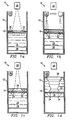
- FIGUREs 1 through 4 of the drawings like numerals being used for like and corresponding parts of the various drawings.
- FIGUREs 1a through 1e illustrate one sequence of steps for producing a model using the stereolithographic process.
- An SLA similar to that depicted in FIGUREs 1a through 1e, may be purchased from 3D Systems, Inc. of Valencia, California or from Quadrax Laser Technologies, Inc. of Portsmouth, Rhode Island.
- the 3D Systems' SLA employs a HeCd laser with a wavelength of 325 nm.
- the 3D System differs from the process described above. It successively lowers the working surface below the surface of liquid instead of raising the liquid relative to the working surface. There, the formed object is slowly submerged as it is produced on the surface of the liquid.
- the Quadrax Laser Technologies' SLA uses an argon-ion visible light laser in the process described in connection with FIGUREs 1a-1c. Other SLA designers use ultraviolet ("UV”) lasers to harden stereolithographic liquids.
- UV ultraviolet
- FIGURE 2 is a partially perspective, partially schematic illustration of an exposure head 20 containing one embodiment of the disclosed invention for use in the process depicted in FIGURE, 1a through 1e.
- the exposure head 20 comprises an illumination source 30 an area array deformable micromirror device (“DMD") 32, two lenses 34 and 36, and control circuitry 38.
- Illumination source 30 emits radiation that is operable to harden a particular SLA liquid.
- Lens 34 more uniformly illuminates DMD 32 than would otherwise occur without it.
- Lens 36 focuses and magnifies the light reflected off of DMD 32 onto the working surface 16 (shown in FIGUREs 1a-1e).
- DMD 32 is an electro-optical device containing a regular nxm array of micromirror manufactured by Texas Instruments, Inc. of Dallas, Texas.
- Each mirror may be electronically controlled to reflect incident radiation along one of a plurality of optical pathways.
- DMD 32 comprises a matrix of bistable mirrors, i.e., there are two optical pathways for each mirror.
- Illumination source 30, DMD 32, and lenses 34 and 36 are positioned such that light impinging upon DMD 32 from illumination source 30 may be focused onto a thin film of SLA resin if, and only if, one of the two optical pathways is selected.
- the optical pathway of radiation emitted from illumination source 30 is depicted by the converging and diverging dashed lines.
- Each bistable mirror on DMD 32 is controlled by circuitry 38 which interprets data from a processor (not shown). Circuitry 38 may be located elsewhere or may be integrated completely with a standalone processor.
- Illumination source 30 may be tailored to the individual stereolithographic liquid used in the SLA process and might be an ordinary tungsten-halogen incandescent light bulb or any number of visible or non-visible light lasers.
- FIGURE 3 depicts perspectively an area array deformable micromirror device 32 illustrated in the exposure head 20 of FIGURE 2.
- DMD 32 comprises a body 40 having a planar active surface 42 and a number of electrical pins 44.
- the active surface 42 of DMD 32 may contain an nxm matrix of individually addressable bistable micromirror.
- Each micromirror is typically a square or diamond having sides of 12 to 20 microns. This small size allows a single DMD having a footprint of approximately 1290 mm 2 (2 square inches) to have over 2 million individually addressable mirrors in, for instance, a 1920 x 1080 matrix.
- This small micromirror size allows exposure head 20 (shown in FIGURE 2) to cure a 101 x 202 mm 2 (4 x 8 square inch) area in a single exposure interval with the same resolution as achieved by prior x-y scanner/laser exposure head combinations.
- theme prior exposure heads achieve resolutions of ⁇ 0,13 mm of ( ⁇ 0.005 inches).
- lens 36 of FIGURE 2 would also magnify the image of DMD 32 by a factor of 4x-6x.
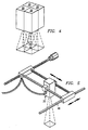
- FIGURE 4 depicts how multiple exposure heads 20 may be combined or "tiled" to cover an area of, for instance, 203 x 406 mm (8 x 16 square inch). This allows the user to maintain the same high degree of resolution described in connection with FIGURE 3.
- each exposure head 20 cures one quadrant of the film resin. Each quadrant exposes a 101 x 202 mm 2 (4 x 8 square inch) area. Any number of exposure heads 20 can be combined to increase maximum model size.
- FIGURE 5 depicts how a single exposure head 20 may be mounted on a positioning device 46 with freedom of movement in two dimensions.
- the single exposure head 20 may thereby be made to cure a lamina of resin larger in size than the projected image of DMD 32 (FIGUREs 2 and 3). This allows the user to maintain the same high degree of resolution described in connection with FIGURE 3.
- Positioning devices used in lithographic processes are known in the art to have resolutions comparable with the SLA process. These positioning devices are used to align photomasks with silicon wafers in the production of devices such as integrated circuits.
Landscapes
- Physics & Mathematics (AREA)
- Chemical & Material Sciences (AREA)
- Engineering & Computer Science (AREA)
- Materials Engineering (AREA)
- General Physics & Mathematics (AREA)
- Manufacturing & Machinery (AREA)
- Optics & Photonics (AREA)
- Mechanical Engineering (AREA)
- Exposure And Positioning Against Photoresist Photosensitive Materials (AREA)
- Mechanical Light Control Or Optical Switches (AREA)
- Heating, Cooling, Or Curing Plastics Or The Like In General (AREA)
Description
- This invention relates to a stereolithographic apparatus as defined in the precharacterizing part of
claim 1 and to a method as defined in the precharacterizing part of claim 9. - A stereolithographic apparatus and a method as mentioned above are known from WO-A-91/12120. This document describes a method and apparatus for forming a solid three-dimensional article by exposure of successive layers of a liquid material to a vertically movable energy source. The apparatus includes a fixed support plate disposed in a container, the liquid being dispensed to successively higher levels in the container above the plate. In one embodiment, the liquid is fed from a reservoir below the plate to an upper portion of the container above the plate by an expandable member disposed in the reservoir. A vertically movable liquid dispenser may be provided above the plate either alone or in combination with the expandable member. The energy source includes a laser, a focusing optics system and a scanner head for directing a laser beam to solidify selected portions of successive layers of the liquid medium.
- Stereolithography is a process by which three dimensional objects are fabricated from thin layers of hardened or cured liquid polymers. The liquid polymers or resins are selectively hardened by an intense light source of suitable wave length. Typically, an ultraviolet ("UV"), argon-ion, or other type of laser is used to harden the liquid polymer. The particular laser is directed to a thin film of the polymer by an x-y scanner interpreting, typically, computer-aided design ("CAD") data. The CAD data mathematically represents the shape of the object to be produced as a series of sequential thin layers of laminas, typically 1/100th of an inch in thickness. The object may thereby be produced by curing portions of a film of resin that correspond to the first layer of the object, by coating the hardened layer with a uniform thin liquid film, and by curing portions of the second film that correspond to the next lamina of the object. This process is repeated until each lamina of the model has been reproduced as a layer of hardened polymer. The model produced by stereolithography may be used for testing and evaluation of engineering designs, for tooling purposes and for low volume manufacturing applications.
- Known stereolithographic process devices and methods are limited by at least two characteristics. First, the use of an x-y scanner limits the speed by which a laser beam may be scanned on to a film of liquid resin to approximately 55 inches per second. This speed, coupled with the high vertical resolution of the process, results in lengthy production time and low product output. Second, the use of a particular laser as the illumination source limits the type of liquid resin that may be used in the system. Each resin has an individual reaction to various wavelengths of electromagnetic radiation.
- Typically, each resin may be hardened by only one type of laser. This results in little or no ability to change the resin composition without expensive hardware changes. Also, not all wavelengths of radiation may be produced as laser light. This precludes the use of certain resins because no laser exists to cure them.
- In EP-A-0 450 762 a solid imaging apparatus and method is described which produces an integral three-dimensional object from a multiplicity of cross sectional portions of the object by selectively exposing successive layers of a liquid photoformable composition to actinic radiation. The apparatus includes a vessel for containing the composition so as to present a free surface, and a movable platform disposed within the vessel below the free surface. Part of the composition is transferred above the free surface, by lowering and raising a dispenser at predetermined positions located away from the platform. A doctor blade contacts the composition transferred above the free surface and then moves over the platform to form a substantially uniform layer of the composition.
- Document EP-A-0 391 529 describes a visual display system having a spatial light modulator with individually and simultaneously controllable elements. Each element capable of producing an individual light beam directed toward a display surface. A source of random polarity light is utilized to direct light onto the modulator.
- Document WO-A-89/09687 relates to a system for producing precision plastic products via the polymerisation of liquid plastics using focussed ultra-violet laser beams whose computer controlled positioning relative to the face of a computer controlled adjustable piston immersed in the said liquid plastic allows for the hardened plastic product been produced to rest on the said end face of said piston as the computer controlled laser beam product profiling processes take place within the liquid plastic. The system is particularly suitable for the transformation of a computer software product design into a three dimensional, hard plastic copy. The system has application in the production of all-plastic credit and identification cards, plastic models of buildings, toys, letters, numbers, tools, moulds and dies.
- Therefore, a need has arisen for a stereolithographic apparatus which allows for high product output and which is compatible with a wider range stereolithographic resins.
- The object of the invention is to provide a fast, flexible, low cost stereolithographic apparatus particularly suited to large model fabrication.
- In accordance with the present invention the above object is achieved by a stereolithographic apparatus having the features of
claim 1. - In accordance with the present invention, the above object is further achieved by a method of forming a model of cured resin having the features of claim 9.
- Particular embodiments of the invention are disclosed in the dependent claims.
- A stereolithographic apparatus is disclosed comprising a vat for receiving a stereolithographic liquid, a working surface within said vat, an elevating mechanism for controlling the level of the liquid in the vat relative to the working surface, an illumination source for emitting radiation, and a deformable micromirror device. The illumination source emits radiation which is operable to harden the liquid, while the deformable micromirror device is operable to reflect the incident radiation onto the surface of the liquid.
- The first technical advantage of the disclosed invention is its speed. The plurality of micromirror which comprise the deformable micromirror device allow an entire layer of resin to be hardened in one exposure interval. This technique allows much greater throughput.
- A second technical advantage of the device is its flexibility. Almost any illumination source may be used with the deformable micromirror device. The illumination source can therefore be tailored to the particular resin so used and may, in fact, be an inexpensive incandescent light bulb.
- A third technical advantage of the disclosed invention is its cost. Deformable micromirror devices are currently available in mass produced quantities at costs far below that of an x-y laser scanner.
- Another technical advantage of the invention is its suitability to large model fabrication. Multiple exposure heads may be combined to cure a large layer of a livid or a single exposure head may be positioned to cure the same large area in a few exposure intervals. Resolution will meanwhile remain high.
- For a more complete understanding of the present invention and the advantages thereof, reference is now made to the following description taken in conjunction with the accompanying drawings in which:
- FIGUREs 1a through 1e illustrate one sequence of steps for producing a model using the stereolithographic process;
- FIGURE 2 is a partially perspective, partially schematic illustration of an exposure head containing one embodiment of the disclosed invention for use in the process depicted in FIGUREs 1a through 1e;
- FIGURE 3 depicts perspectively an area array deformable micromirror device useful in the exposure head of FIGURE 2;
- FIGURE 4 depicts schematically how the exposure head of FIGURE 2 may be combined with similar exposure heads to increase possible model size; and
- FIGURE 5 depicts perspectively how the exposure head of FIGURE 2 may be articulated to cure a larger film size.
- The preferred embodiment of the present invention and its advantages are best understood by referring to FIGUREs 1 through 4 of the drawings, like numerals being used for like and corresponding parts of the various drawings.
- FIGUREs 1a through 1e illustrate one sequence of steps for producing a model using the stereolithographic process.
- (a) Stereolithographic apparatus ("SLA") 10 comprises
vat 12 for receiving a stereolithographic liquid 14, a workingsurface 16, anelevator 18 for controlling the level of the liquid relative to the workingsurface 16, and anexposure head 20 for curing selected portions of the resin as will be described more fully below. The stereolithographic liquid may be a resin or a polymer, as is well known to those skilled in the art.SLA 10 may also comprise aliquid applicator 22 for ensuring a uniform liquid thickness at each modeling stage.
In operation, a thin film of liquid is applied to workingsurface 16 by, for instance, raisingelevator 18 withinvat 12.Elevator 18 will cause liquid 14 to rise throughperforations 24 to form a thin film on workingsurface 16.Exposure head 20 then cures selected portions of the liquid film by directing electromagnetic radiation thereto.Exposure head 20 is controlled by circuitry (shown in FIGURE 2) that interprets data of the object to be so modeled. The data represents the object as a series of thin sequential layers or laminas which, when stacked on top of each other form the complete object. Typically, computer-aided design ("CAD") data may be moot easily converted into sequential layers or laminas of the model to be produced. - (b)
Elevator 18 again rises to cause liquid 14 to cover the previously cured layer 26 ("workpiece") resting on workingsurface 26 with a second film of liquid. This second layer of liquid will cover both the cured and uncured portions of the first layer.Applicator 22 may also spray a small amount of liquid ontoworkpiece 26 to ensure uniform film coverage of theworkpiece 26. Each film is approximately 0,25 mm (one 1/100th of an inch) thick. - (c)
Exposure head 26 cures the second layer of liquid applied in FIGURE 1b as described in connection with FIGURE 1a. - (d) The steps in FIGUREs 1a through 1c are then repeated until the
entire part 28 has been produced. - (e)
Complete part 28 may then be removed fromSLA 10. Under certain conditions using certain liquids, it may be necessary to curepart 28 in an oven (not shown) prior to its use. - An SLA, similar to that depicted in FIGUREs 1a through 1e, may be purchased from 3D Systems, Inc. of Valencia, California or from Quadrax Laser Technologies, Inc. of Portsmouth, Rhode Island. The 3D Systems' SLA employs a HeCd laser with a wavelength of 325 nm. The 3D System differs from the process described above. It successively lowers the working surface below the surface of liquid instead of raising the liquid relative to the working surface. There, the formed object is slowly submerged as it is produced on the surface of the liquid. The Quadrax Laser Technologies' SLA uses an argon-ion visible light laser in the process described in connection with FIGUREs 1a-1c. Other SLA designers use ultraviolet ("UV") lasers to harden stereolithographic liquids.
- FIGURE 2 is a partially perspective, partially schematic illustration of an
exposure head 20 containing one embodiment of the disclosed invention for use in the process depicted in FIGURE, 1a through 1e. Theexposure head 20 comprises anillumination source 30 an area array deformable micromirror device ("DMD") 32, twolenses control circuitry 38.Illumination source 30 emits radiation that is operable to harden a particular SLA liquid.Lens 34 more uniformly illuminatesDMD 32 than would otherwise occur without it.Lens 36 focuses and magnifies the light reflected off ofDMD 32 onto the working surface 16 (shown in FIGUREs 1a-1e).DMD 32 is an electro-optical device containing a regular nxm array of micromirror manufactured by Texas Instruments, Inc. of Dallas, Texas. Each mirror may be electronically controlled to reflect incident radiation along one of a plurality of optical pathways. In the preferred embodiment,DMD 32 comprises a matrix of bistable mirrors, i.e., there are two optical pathways for each mirror.Illumination source 30,DMD 32, andlenses DMD 32 fromillumination source 30 may be focused onto a thin film of SLA resin if, and only if, one of the two optical pathways is selected. The optical pathway of radiation emitted fromillumination source 30 is depicted by the converging and diverging dashed lines. Each bistable mirror onDMD 32 is controlled bycircuitry 38 which interprets data from a processor (not shown).Circuitry 38 may be located elsewhere or may be integrated completely with a standalone processor.Illumination source 30 may be tailored to the individual stereolithographic liquid used in the SLA process and might be an ordinary tungsten-halogen incandescent light bulb or any number of visible or non-visible light lasers. - FIGURE 3 depicts perspectively an area array
deformable micromirror device 32 illustrated in theexposure head 20 of FIGURE 2.DMD 32 comprises abody 40 having a planaractive surface 42 and a number ofelectrical pins 44. Theactive surface 42 ofDMD 32 may contain an nxm matrix of individually addressable bistable micromirror. Each micromirror is typically a square or diamond having sides of 12 to 20 microns. This small size allows a single DMD having a footprint of approximately 1290 mm2 (2 square inches) to have over 2 million individually addressable mirrors in, for instance, a 1920 x 1080 matrix. This small micromirror size allows exposure head 20 (shown in FIGURE 2) to cure a 101 x 202 mm2 (4 x 8 square inch) area in a single exposure interval with the same resolution as achieved by prior x-y scanner/laser exposure head combinations. Typically, theme prior exposure heads achieve resolutions of ± 0,13 mm of (± 0.005 inches). In such a case,lens 36 of FIGURE 2 would also magnify the image ofDMD 32 by a factor of 4x-6x. - FIGURE 4 depicts how multiple exposure heads 20 may be combined or "tiled" to cover an area of, for instance, 203 x 406 mm (8 x 16 square inch). This allows the user to maintain the same high degree of resolution described in connection with FIGURE 3. In such a tiled configuration, each
exposure head 20 cures one quadrant of the film resin. Each quadrant exposes a 101 x 202 mm2 (4 x 8 square inch) area. Any number of exposure heads 20 can be combined to increase maximum model size. - FIGURE 5 depicts how a
single exposure head 20 may be mounted on apositioning device 46 with freedom of movement in two dimensions. Thesingle exposure head 20 may thereby be made to cure a lamina of resin larger in size than the projected image of DMD 32 (FIGUREs 2 and 3). This allows the user to maintain the same high degree of resolution described in connection with FIGURE 3. Positioning devices used in lithographic processes are known in the art to have resolutions comparable with the SLA process. These positioning devices are used to align photomasks with silicon wafers in the production of devices such as integrated circuits. - Although the present invention has been described in detail, it should be understood that various changes, substitutions and operations can be made hereto without departing from the scope of the invention as defined by the appended claims.
Claims (10)
- A stereolithographic apparatus (10) comprising a vat (12) for receiving a stereolithographic liquid (14), a working surface (16) within said vat (12), an elevating mechanism (18) for controlling the level of the liquid in the vat (12) relative to the working surface (16), said stereolithographic apparatus characterized byat least one exposure head (20), each exposure head (20) comprising an illumination source for emitting radiation, the radiation operable to harden the liquid, and an area array deformable micromirror device (32) responsive to applied signals for selectively reflecting the radiation to form an image on the surface of the liquid (14).
- The stereolithographic apparatus of claim 1 further comprising a lens (36) for magnifying the image of the area array deformable micromirror device (32).
- The stereolithographic system of claim 1 further comprising a positioner (46) for moving the exposure head (20) in two dimensions.
- The stereolithographic apparatus of claim 3 further comprising a lens (36) for magnifying the image of the area array deformable micromirror device (32).
- The stereolithographic apparatus of claim 1 wherein the elevator (18) raises the liquid (14) relative to the working surface (16).
- The stereolithographic apparatus of claim 1 wherein the elevator (18) lowers the working surface (16) into the liquid (14).
- The stereolithographic apparatus of claim 1 wherein the liquid (14) is a resin containing a photoactive agent.
- The stereolithographic apparatus of claim 1 wherein the liquid (14) is a polymer containing a photoactive agent.
- A method of forming a model (26; 28) of cured resin comprising the sequential repetition of the steps of applying a thin film of stereolithographic liquid (14) to a working surface (16), characterized by the further steps of:illuminating a plurality of micromirrors of an area array deformable micromirror device (32) with radiation operable to cure the liquid resin;deflecting certain of the micromirrors such that a portion of the radiation is directed to the film of liquid (14), said directed radiation curing a portion of the resin, the portion of the resin forming at least part of a lamina of the model (26; 28).
- The method of claim 9 further comprising the steps of:moving the area array deformable micromirror device (32), wherein said device (32) is mounted on a positioning device (46) such that said device (32) illuminates a previously unexposed area of the resin; andcuring said unexposed portion of said resin to form a portion of the lamina of the model.
Priority Applications (1)
| Application Number | Priority Date | Filing Date | Title |
|---|---|---|---|
| EP95106721A EP0676275B1 (en) | 1991-12-30 | 1992-12-22 | Stereolithographic exposure head |
Applications Claiming Priority (2)
| Application Number | Priority Date | Filing Date | Title |
|---|---|---|---|
| US07/814,859 US5247180A (en) | 1991-12-30 | 1991-12-30 | Stereolithographic apparatus and method of use |
| US814859 | 1991-12-30 |
Related Child Applications (2)
| Application Number | Title | Priority Date | Filing Date |
|---|---|---|---|
| EP95106721A Division EP0676275B1 (en) | 1991-12-30 | 1992-12-22 | Stereolithographic exposure head |
| EP95106721.4 Division-Into | 1995-05-04 |
Publications (2)
| Publication Number | Publication Date |
|---|---|
| EP0549993A1 EP0549993A1 (en) | 1993-07-07 |
| EP0549993B1 true EP0549993B1 (en) | 1997-03-26 |
Family
ID=25216187
Family Applications (2)
| Application Number | Title | Priority Date | Filing Date |
|---|---|---|---|
| EP92121770A Expired - Lifetime EP0549993B1 (en) | 1991-12-30 | 1992-12-22 | Stereolithographic apparatus and method of forming a model |
| EP95106721A Expired - Lifetime EP0676275B1 (en) | 1991-12-30 | 1992-12-22 | Stereolithographic exposure head |
Family Applications After (1)
| Application Number | Title | Priority Date | Filing Date |
|---|---|---|---|
| EP95106721A Expired - Lifetime EP0676275B1 (en) | 1991-12-30 | 1992-12-22 | Stereolithographic exposure head |
Country Status (7)
| Country | Link |
|---|---|
| US (1) | US5247180A (en) |
| EP (2) | EP0549993B1 (en) |
| JP (1) | JPH0639928A (en) |
| KR (1) | KR100252458B1 (en) |
| CA (1) | CA2086157A1 (en) |
| DE (2) | DE69231229T2 (en) |
| TW (1) | TW214584B (en) |
Cited By (10)
| Publication number | Priority date | Publication date | Assignee | Title |
|---|---|---|---|---|
| US7467939B2 (en) | 2006-05-03 | 2008-12-23 | 3D Systems, Inc. | Material delivery tension and tracking system for use in solid imaging |
| US7614866B2 (en) | 2007-01-17 | 2009-11-10 | 3D Systems, Inc. | Solid imaging apparatus and method |
| US7706910B2 (en) | 2007-01-17 | 2010-04-27 | 3D Systems, Inc. | Imager assembly and method for solid imaging |
| US7731887B2 (en) | 2007-01-17 | 2010-06-08 | 3D Systems, Inc. | Method for removing excess uncured build material in solid imaging |
| US7771183B2 (en) | 2007-01-17 | 2010-08-10 | 3D Systems, Inc. | Solid imaging system with removal of excess uncured build material |
| US7931460B2 (en) | 2006-05-03 | 2011-04-26 | 3D Systems, Inc. | Material delivery system for use in solid imaging |
| US8003039B2 (en) | 2007-01-17 | 2011-08-23 | 3D Systems, Inc. | Method for tilting solid image build platform for reducing air entrainment and for build release |
| US8105066B2 (en) | 2007-01-17 | 2012-01-31 | 3D Systems, Inc. | Cartridge for solid imaging apparatus and method |
| US8221671B2 (en) | 2007-01-17 | 2012-07-17 | 3D Systems, Inc. | Imager and method for consistent repeatable alignment in a solid imaging apparatus |
| EP3181357A1 (en) | 2015-12-15 | 2017-06-21 | Agfa Graphics NV | Addiditve manufacturing method using dynamic light projection for flexographic print masters |
Families Citing this family (130)
| Publication number | Priority date | Publication date | Assignee | Title |
|---|---|---|---|---|
| US6219015B1 (en) | 1992-04-28 | 2001-04-17 | The Board Of Directors Of The Leland Stanford, Junior University | Method and apparatus for using an array of grating light valves to produce multicolor optical images |
| WO1995015841A1 (en) * | 1992-06-05 | 1995-06-15 | Finab Limited | Machine for making objects by selectively photopolymerising layered liquids or powders |
| US6467345B1 (en) | 1993-10-18 | 2002-10-22 | Xros, Inc. | Method of operating micromachined members coupled for relative rotation |
| US6044705A (en) * | 1993-10-18 | 2000-04-04 | Xros, Inc. | Micromachined members coupled for relative rotation by torsion bars |
| AU2908895A (en) * | 1994-06-27 | 1996-01-19 | Hercules Incorporated | Programmable mask for producing three-dimensional objects |
| US5573721A (en) * | 1995-02-16 | 1996-11-12 | Hercules Incorporated | Use of a support liquid to manufacture three-dimensional objects |
| US5841579A (en) | 1995-06-07 | 1998-11-24 | Silicon Light Machines | Flat diffraction grating light valve |
| US5691541A (en) * | 1996-05-14 | 1997-11-25 | The Regents Of The University Of California | Maskless, reticle-free, lithography |
| GB2315700A (en) * | 1996-07-27 | 1998-02-11 | Rupert Charles David Young | Use of dynamic masks for object manufacture |
| JP2818934B2 (en) * | 1996-12-02 | 1998-10-30 | マツダ株式会社 | Stratified charge engine |
| WO1998029782A1 (en) * | 1996-12-31 | 1998-07-09 | Luellau Friedrich | Method for controlling an exposure device |
| US6051179A (en) * | 1997-03-19 | 2000-04-18 | Replicator Systems, Inc. | Apparatus and method for production of three-dimensional models by spatial light modulator |
| US5982553A (en) | 1997-03-20 | 1999-11-09 | Silicon Light Machines | Display device incorporating one-dimensional grating light-valve array |
| US6088102A (en) | 1997-10-31 | 2000-07-11 | Silicon Light Machines | Display apparatus including grating light-valve array and interferometric optical system |
| DE69909972T2 (en) * | 1998-02-11 | 2004-05-13 | University Of Houston, Houston | DEVICE FOR CARRYING OUT CHEMICAL AND BIOCHEMICAL REACTIONS USING PHOTO-GENERATED REAGENTS |
| US20040035690A1 (en) * | 1998-02-11 | 2004-02-26 | The Regents Of The University Of Michigan | Method and apparatus for chemical and biochemical reactions using photo-generated reagents |
| US6271808B1 (en) | 1998-06-05 | 2001-08-07 | Silicon Light Machines | Stereo head mounted display using a single display device |
| US6130770A (en) | 1998-06-23 | 2000-10-10 | Silicon Light Machines | Electron gun activated grating light valve |
| US6101036A (en) | 1998-06-23 | 2000-08-08 | Silicon Light Machines | Embossed diffraction grating alone and in combination with changeable image display |
| US6215579B1 (en) | 1998-06-24 | 2001-04-10 | Silicon Light Machines | Method and apparatus for modulating an incident light beam for forming a two-dimensional image |
| US6303986B1 (en) | 1998-07-29 | 2001-10-16 | Silicon Light Machines | Method of and apparatus for sealing an hermetic lid to a semiconductor die |
| EP1117478B1 (en) * | 1998-08-28 | 2005-06-01 | Febit AG | Support for a method for determining an analyte and a method for producing the support |
| US7620527B1 (en) | 1999-05-10 | 2009-11-17 | Johan Leo Alfons Gielis | Method and apparatus for synthesizing and analyzing patterns utilizing novel “super-formula” operator |
| US6626949B1 (en) | 1999-07-14 | 2003-09-30 | Biopro, Inc. | Diamond coated joint implant |
| DE19944760A1 (en) * | 1999-09-17 | 2001-03-22 | Basys Print Gmbh Systeme Fuer | Device and method for compensating for inhomogeneities in imaging systems |
| CA2388046A1 (en) | 1999-11-05 | 2001-05-17 | Z Corporation | Material systems and methods of three-dimensional printing |
| JP2001188354A (en) * | 1999-12-28 | 2001-07-10 | Asahi Kasei Corp | Method for manufacturing photosensitive resin letterpress and apparatus for manufacturing the same |
| US6369845B1 (en) | 2000-03-14 | 2002-04-09 | Kubota Research Associates Inc. | Exposure system for recording media |
| US6816182B2 (en) * | 2000-03-14 | 2004-11-09 | Masanori Kubota | Radiation welding and imaging apparatus and method for using the same |
| US6500378B1 (en) | 2000-07-13 | 2002-12-31 | Eom Technologies, L.L.C. | Method and apparatus for creating three-dimensional objects by cross-sectional lithography |
| DE10051396A1 (en) * | 2000-10-17 | 2002-04-18 | Febit Ferrarius Biotech Gmbh | An integrated synthesis and identification of an analyte, comprises particles immobilized at a carrier to be coupled to receptors in a structured pattern to give receptor arrays for biochemical reactions |
| US20020160427A1 (en) * | 2001-04-27 | 2002-10-31 | Febit Ag | Methods and apparatuses for electronic determination of analytes |
| US6747781B2 (en) | 2001-06-25 | 2004-06-08 | Silicon Light Machines, Inc. | Method, apparatus, and diffuser for reducing laser speckle |
| US6782205B2 (en) | 2001-06-25 | 2004-08-24 | Silicon Light Machines | Method and apparatus for dynamic equalization in wavelength division multiplexing |
| DE10130968B4 (en) * | 2001-06-27 | 2009-08-20 | Envisiontec Gmbh | Coated polymeric material, its use and process for its preparation |
| US6829092B2 (en) | 2001-08-15 | 2004-12-07 | Silicon Light Machines, Inc. | Blazed grating light valve |
| US6800238B1 (en) | 2002-01-15 | 2004-10-05 | Silicon Light Machines, Inc. | Method for domain patterning in low coercive field ferroelectrics |
| AU2003226932B2 (en) * | 2002-04-09 | 2008-10-30 | Sign-Tronic Ag | Light modulating engine |
| US6855482B2 (en) * | 2002-04-09 | 2005-02-15 | Day International, Inc. | Liquid transfer articles and method for producing the same using digital imaging photopolymerization |
| IL164483A0 (en) * | 2002-04-10 | 2005-12-18 | Fujinon Corp | Exposure head, exposure apparatus, and applicationthereof |
| US6767751B2 (en) | 2002-05-28 | 2004-07-27 | Silicon Light Machines, Inc. | Integrated driver process flow |
| US6822797B1 (en) | 2002-05-31 | 2004-11-23 | Silicon Light Machines, Inc. | Light modulator structure for producing high-contrast operation using zero-order light |
| US6829258B1 (en) | 2002-06-26 | 2004-12-07 | Silicon Light Machines, Inc. | Rapidly tunable external cavity laser |
| US6714337B1 (en) | 2002-06-28 | 2004-03-30 | Silicon Light Machines | Method and device for modulating a light beam and having an improved gamma response |
| US6813059B2 (en) | 2002-06-28 | 2004-11-02 | Silicon Light Machines, Inc. | Reduced formation of asperities in contact micro-structures |
| US6801354B1 (en) | 2002-08-20 | 2004-10-05 | Silicon Light Machines, Inc. | 2-D diffraction grating for substantially eliminating polarization dependent losses |
| US6712480B1 (en) | 2002-09-27 | 2004-03-30 | Silicon Light Machines | Controlled curvature of stressed micro-structures |
| US6806997B1 (en) | 2003-02-28 | 2004-10-19 | Silicon Light Machines, Inc. | Patterned diffractive light modulator ribbon for PDL reduction |
| US6829077B1 (en) | 2003-02-28 | 2004-12-07 | Silicon Light Machines, Inc. | Diffractive light modulator with dynamically rotatable diffraction plane |
| MXPA06010811A (en) * | 2004-03-22 | 2006-12-19 | Thomson Licensing | Method and apparatus for improving images provided by spatial light modulated (slm) display systems. |
| US7250632B2 (en) * | 2004-04-06 | 2007-07-31 | E. I. Du Pont De Nemours And Company | Electronic devices having a layer overlying an edge of a different layer and a process for forming the same |
| DE102004022606A1 (en) * | 2004-05-07 | 2005-12-15 | Envisiontec Gmbh | Method for producing a three-dimensional object with improved separation of hardened material layers from a building level |
| DE102004022961B4 (en) * | 2004-05-10 | 2008-11-20 | Envisiontec Gmbh | Method for producing a three-dimensional object with resolution improvement by means of pixel shift |
| EP1744871B1 (en) | 2004-05-10 | 2008-05-07 | Envisiontec GmbH | Method for producing a three-dimensional object with resolution enhancement by means of pixel shift |
| US7758799B2 (en) * | 2005-04-01 | 2010-07-20 | 3D Systems, Inc. | Edge smoothness with low resolution projected images for use in solid imaging |
| CA2607368A1 (en) * | 2005-05-20 | 2006-11-23 | Huntsman Advanced Materials (Switzerland) Gmbh | Rapid prototyping apparatus and method of rapid prototyping |
| CN100340844C (en) * | 2005-12-07 | 2007-10-03 | 西安交通大学 | Resin level detection method for ultraviolet curing quick forming process |
| DE102006019963B4 (en) * | 2006-04-28 | 2023-12-07 | Envisiontec Gmbh | Device and method for producing a three-dimensional object by layer-by-layer solidifying a material that can be solidified under the influence of electromagnetic radiation using mask exposure |
| DE102006019964C5 (en) * | 2006-04-28 | 2021-08-26 | Envisiontec Gmbh | Device and method for producing a three-dimensional object by means of mask exposure |
| US7636610B2 (en) * | 2006-07-19 | 2009-12-22 | Envisiontec Gmbh | Method and device for producing a three-dimensional object, and computer and data carrier useful therefor |
| US9415544B2 (en) * | 2006-08-29 | 2016-08-16 | 3D Systems, Inc. | Wall smoothness, feature accuracy and resolution in projected images via exposure levels in solid imaging |
| US7892474B2 (en) | 2006-11-15 | 2011-02-22 | Envisiontec Gmbh | Continuous generative process for producing a three-dimensional object |
| EP2089215B1 (en) | 2006-12-08 | 2015-02-18 | 3D Systems Incorporated | Three dimensional printing material system |
| WO2008086033A1 (en) | 2007-01-10 | 2008-07-17 | Z Corporation | Three-dimensional printing material system with improved color, article performance, and ease of use |
| US20080226346A1 (en) * | 2007-01-17 | 2008-09-18 | 3D Systems, Inc. | Inkjet Solid Imaging System and Method for Solid Imaging |
| CN101626881B (en) * | 2007-01-17 | 2012-11-14 | 3D系统公司 | Imager assembly and method for solid imaging |
| US20080181977A1 (en) * | 2007-01-17 | 2008-07-31 | Sperry Charles R | Brush assembly for removal of excess uncured build material |
| US20080170112A1 (en) * | 2007-01-17 | 2008-07-17 | Hull Charles W | Build pad, solid image build, and method for building build supports |
| US7968626B2 (en) | 2007-02-22 | 2011-06-28 | Z Corporation | Three dimensional printing material system and method using plasticizer-assisted sintering |
| US20100140849A1 (en) * | 2007-03-22 | 2010-06-10 | Stratasys, Inc. | Extrusion-based layered deposition systems using selective radiation exposure |
| EP2011631B1 (en) | 2007-07-04 | 2012-04-18 | Envisiontec GmbH | Process and device for producing a three-dimensional object |
| DK2052693T4 (en) | 2007-10-26 | 2021-03-15 | Envisiontec Gmbh | Process and free-form manufacturing system to produce a three-dimensional object |
| DE102008009003A1 (en) * | 2008-02-13 | 2009-08-20 | Dreve Prodimed Gmbh | Apparatus and method for the generative production of 3-dimensional objects based on a multi-phase system |
| GB0816258D0 (en) * | 2008-09-05 | 2008-10-15 | Ulive Entpr Ltd | Process |
| US8048359B2 (en) | 2008-10-20 | 2011-11-01 | 3D Systems, Inc. | Compensation of actinic radiation intensity profiles for three-dimensional modelers |
| US8372330B2 (en) | 2009-10-19 | 2013-02-12 | Global Filtration Systems | Resin solidification substrate and assembly |
| GB201016169D0 (en) | 2010-09-27 | 2010-11-10 | Materialise Nv | Method for reducing differential shrinkage in stereolithography |
| JP5905477B2 (en) | 2010-10-27 | 2016-04-20 | ファイル2パート インコーポレイテッド | 3D object modeling process and modeling equipment |
| WO2012166953A1 (en) * | 2011-05-31 | 2012-12-06 | Nanoptics, Incorporated | Method and apparatus for lithographic manufacture of multi-component polymeric fiber plates |
| US8691476B2 (en) | 2011-12-16 | 2014-04-08 | Taiwan Semiconductor Manufacturing Company, Ltd. | EUV mask and method for forming the same |
| US9636873B2 (en) | 2012-05-03 | 2017-05-02 | B9Creations, LLC | Solid image apparatus with improved part separation from the image plate |
| CA2885954A1 (en) | 2012-09-24 | 2014-03-27 | The Antenna Company International N.V. | Lens antenna, method of manufacturing and using such an antenna, and antenna system |
| US9034237B2 (en) | 2012-09-25 | 2015-05-19 | 3D Systems, Inc. | Solid imaging systems, components thereof, and methods of solid imaging |
| FR3000698B1 (en) * | 2013-01-09 | 2015-02-06 | Phidias Technologies | FABRICATION OF A VOLUME OBJECT BY LITHOGRAPHY, WITH IMPROVED SPATIAL RESOLUTION |
| US9498920B2 (en) | 2013-02-12 | 2016-11-22 | Carbon3D, Inc. | Method and apparatus for three-dimensional fabrication |
| WO2014126837A2 (en) | 2013-02-12 | 2014-08-21 | Eipi Systems, Inc. | Continuous liquid interphase printing |
| US9321215B2 (en) | 2013-03-12 | 2016-04-26 | Orange Maker, Llc | 3D printing using spiral buildup |
| US12083744B2 (en) | 2013-03-12 | 2024-09-10 | Orange Maker, Llc | Security features and anti-counterfeiting and part tracking system for 3D printed parts |
| US11141908B2 (en) * | 2013-03-12 | 2021-10-12 | Orange Maker LLC | 3D printing using rotational components and improved light sources |
| US10150247B2 (en) * | 2013-03-12 | 2018-12-11 | Orange Maker LLC | 3D printing using spiral buildup and high viscosity build materials |
| US10335901B2 (en) * | 2013-06-10 | 2019-07-02 | Renishaw Plc | Selective laser solidification apparatus and method |
| GB201310398D0 (en) | 2013-06-11 | 2013-07-24 | Renishaw Plc | Additive manufacturing apparatus and method |
| US9360757B2 (en) | 2013-08-14 | 2016-06-07 | Carbon3D, Inc. | Continuous liquid interphase printing |
| US11260208B2 (en) | 2018-06-08 | 2022-03-01 | Acclarent, Inc. | Dilation catheter with removable bulb tip |
| US9527244B2 (en) | 2014-02-10 | 2016-12-27 | Global Filtration Systems | Apparatus and method for forming three-dimensional objects from solidifiable paste |
| AU2015226847A1 (en) * | 2014-03-07 | 2016-09-01 | Sgat Pty Ltd | Three dimensional printer |
| CN106463834A (en) | 2014-03-26 | 2017-02-22 | 天线国际有限责任公司 | Patch antenna, method of manufacturing and using such an antenna, and antenna system |
| KR102393361B1 (en) * | 2014-04-15 | 2022-05-03 | 네덜란제 오르가니자티에 포오르 토에게파스트-나투우르베텐샤펠리즈크 온데르조에크 테엔오 | Exposure head, exposure apparatus and method of operating an exposure head |
| US10471699B2 (en) | 2014-06-20 | 2019-11-12 | Carbon, Inc. | Three-dimensional printing with reciprocal feeding of polymerizable liquid |
| WO2015195909A1 (en) * | 2014-06-20 | 2015-12-23 | Carbon3D, Inc. | Three-dimensional printing using tiled light engines |
| CN106687861B (en) | 2014-06-23 | 2022-01-11 | 卡本有限公司 | Method for producing three-dimensional objects from materials with multiple hardening mechanisms |
| GB201505458D0 (en) | 2015-03-30 | 2015-05-13 | Renishaw Plc | Additive manufacturing apparatus and methods |
| DE102015208852A1 (en) | 2015-05-13 | 2016-11-17 | Nanoscribe Gmbh | Method for producing a three-dimensional structure |
| KR20160144837A (en) * | 2015-06-09 | 2016-12-19 | 오스템임플란트 주식회사 | Three dimensional printer and method for operating the same |
| DE102015008863A1 (en) | 2015-07-14 | 2017-01-19 | BXG tech GmbH i. Gr. | Method and device for 3D printing with several installation spaces or an extended installation space |
| US10336056B2 (en) | 2015-08-31 | 2019-07-02 | Colorado School Of Mines | Hybrid additive manufacturing method |
| KR101725658B1 (en) * | 2015-09-08 | 2017-04-27 | 임은석 | Three dimensional printer and method of forming a three dimensional objedt |
| US10792868B2 (en) | 2015-09-09 | 2020-10-06 | Carbon, Inc. | Method and apparatus for three-dimensional fabrication |
| US20180194063A1 (en) * | 2015-09-30 | 2018-07-12 | Hewlett-Packard Development Company, L.P. | Build material containers |
| WO2017066584A1 (en) | 2015-10-15 | 2017-04-20 | Saint-Gobain Ceramics & Plastics, Inc. | Method for forming a three dimensional body from a mixture with a high content of solid particles |
| TWI674964B (en) * | 2015-10-22 | 2019-10-21 | 揚明光學股份有限公司 | Three dimensional printing apparatus and three dimensional printing method |
| AT518101B1 (en) * | 2015-12-17 | 2018-05-15 | Stadlmann Klaus | Method of producing a three-dimensional object |
| US10737479B2 (en) | 2017-01-12 | 2020-08-11 | Global Filtration Systems | Method of making three-dimensional objects using both continuous and discontinuous solidification |
| US10316213B1 (en) | 2017-05-01 | 2019-06-11 | Formlabs, Inc. | Dual-cure resins and related methods |
| DE102017110241A1 (en) | 2017-05-11 | 2018-11-15 | Nanoscribe Gmbh | Method for generating a 3D structure by means of laser lithography and computer program product |
| US10967578B2 (en) | 2017-07-11 | 2021-04-06 | Daniel S. Clark | 5D part growing machine with volumetric display technology |
| US11919246B2 (en) | 2017-07-11 | 2024-03-05 | Daniel S. Clark | 5D part growing machine with volumetric display technology |
| US10953597B2 (en) | 2017-07-21 | 2021-03-23 | Saint-Gobain Performance Plastics Corporation | Method of forming a three-dimensional body |
| EP3758916A4 (en) * | 2018-03-02 | 2021-10-27 | Formlabs, Inc. | Latent cure resins and related methods |
| FI128627B (en) * | 2018-06-28 | 2020-09-15 | Planmeca Oy | Stereolithography apparatus equipped with resin collecting mechanism and method of operating said apparatus |
| CN113508023A (en) * | 2019-01-24 | 2021-10-15 | 沃尔特·沃伊特 | Systems, methods, and materials for ultra-high throughput additive manufacturing |
| EP3930987B1 (en) | 2019-02-28 | 2023-01-25 | 3D Systems, Inc. | High resolution three-dimensional printing system |
| US11951679B2 (en) | 2021-06-16 | 2024-04-09 | General Electric Company | Additive manufacturing system |
| US11731367B2 (en) | 2021-06-23 | 2023-08-22 | General Electric Company | Drive system for additive manufacturing |
| US11958250B2 (en) | 2021-06-24 | 2024-04-16 | General Electric Company | Reclamation system for additive manufacturing |
| US11958249B2 (en) | 2021-06-24 | 2024-04-16 | General Electric Company | Reclamation system for additive manufacturing |
| US11826950B2 (en) | 2021-07-09 | 2023-11-28 | General Electric Company | Resin management system for additive manufacturing |
| US11813799B2 (en) | 2021-09-01 | 2023-11-14 | General Electric Company | Control systems and methods for additive manufacturing |
| WO2023205716A1 (en) | 2022-04-22 | 2023-10-26 | Carbon, Inc. | Hollow dental molds configured for high throughput cleaning |
| WO2023220523A1 (en) | 2022-05-09 | 2023-11-16 | Carbon, Inc. | Method for direct coloration of resins for additive manufacturing |
Family Cites Families (9)
| Publication number | Priority date | Publication date | Assignee | Title |
|---|---|---|---|---|
| IL84936A (en) * | 1987-12-23 | 1997-02-18 | Cubital Ltd | Three-dimensional modelling apparatus |
| US5106288A (en) * | 1988-04-11 | 1992-04-21 | Austral Asian Lasers Pty Ltd. | Laser based plastic model making workstation |
| US5059359A (en) * | 1988-04-18 | 1991-10-22 | 3 D Systems, Inc. | Methods and apparatus for production of three-dimensional objects by stereolithography |
| US5164128A (en) * | 1988-04-18 | 1992-11-17 | 3D Systems, Inc. | Methods for curing partially polymerized parts |
| EP0635986B1 (en) * | 1989-02-27 | 2000-05-10 | Texas Instruments Incorporated | Apparatus and method for digitized video system |
| US5011635A (en) * | 1989-05-18 | 1991-04-30 | Desoto, Inc. | Stereolithographic method and apparatus in which a membrane separates phases |
| ATE185514T1 (en) * | 1990-02-15 | 1999-10-15 | 3D Systems Inc | METHOD AND APPARATUS FOR FORMING A SOLID THREE-DIMENSIONAL ARTICLE FROM A LIQUID |
| CA2036695A1 (en) * | 1990-03-01 | 1991-09-02 | Brian Gregory Chapman | Solid imaging apparatus and method with coating station |
| US5049901A (en) * | 1990-07-02 | 1991-09-17 | Creo Products Inc. | Light modulator using large area light sources |
-
1991
- 1991-12-30 US US07/814,859 patent/US5247180A/en not_active Expired - Lifetime
-
1992
- 1992-12-22 EP EP92121770A patent/EP0549993B1/en not_active Expired - Lifetime
- 1992-12-22 EP EP95106721A patent/EP0676275B1/en not_active Expired - Lifetime
- 1992-12-22 DE DE69231229T patent/DE69231229T2/en not_active Expired - Fee Related
- 1992-12-22 DE DE69218572T patent/DE69218572T2/en not_active Expired - Fee Related
- 1992-12-23 CA CA2086157A patent/CA2086157A1/en not_active Abandoned
- 1992-12-30 KR KR1019920026426A patent/KR100252458B1/en not_active IP Right Cessation
-
1993
- 1993-01-04 JP JP5000111A patent/JPH0639928A/en active Pending
- 1993-05-11 TW TW082103644A patent/TW214584B/zh active
Cited By (12)
| Publication number | Priority date | Publication date | Assignee | Title |
|---|---|---|---|---|
| US7467939B2 (en) | 2006-05-03 | 2008-12-23 | 3D Systems, Inc. | Material delivery tension and tracking system for use in solid imaging |
| US7931460B2 (en) | 2006-05-03 | 2011-04-26 | 3D Systems, Inc. | Material delivery system for use in solid imaging |
| US7614866B2 (en) | 2007-01-17 | 2009-11-10 | 3D Systems, Inc. | Solid imaging apparatus and method |
| US7706910B2 (en) | 2007-01-17 | 2010-04-27 | 3D Systems, Inc. | Imager assembly and method for solid imaging |
| US7731887B2 (en) | 2007-01-17 | 2010-06-08 | 3D Systems, Inc. | Method for removing excess uncured build material in solid imaging |
| US7771183B2 (en) | 2007-01-17 | 2010-08-10 | 3D Systems, Inc. | Solid imaging system with removal of excess uncured build material |
| US8003039B2 (en) | 2007-01-17 | 2011-08-23 | 3D Systems, Inc. | Method for tilting solid image build platform for reducing air entrainment and for build release |
| US8105066B2 (en) | 2007-01-17 | 2012-01-31 | 3D Systems, Inc. | Cartridge for solid imaging apparatus and method |
| US8221671B2 (en) | 2007-01-17 | 2012-07-17 | 3D Systems, Inc. | Imager and method for consistent repeatable alignment in a solid imaging apparatus |
| US8465689B2 (en) | 2007-01-17 | 2013-06-18 | 3D Systems, Inc. | Elevator and method for tilting solid image build platform for reducing air entrainment and for build release |
| EP3181357A1 (en) | 2015-12-15 | 2017-06-21 | Agfa Graphics NV | Addiditve manufacturing method using dynamic light projection for flexographic print masters |
| WO2017102353A1 (en) | 2015-12-15 | 2017-06-22 | Agfa Graphics Nv | Additive manufacturing method using dynamic light projection for flexographic print masters |
Also Published As
| Publication number | Publication date |
|---|---|
| KR100252458B1 (en) | 2000-04-15 |
| EP0676275A1 (en) | 1995-10-11 |
| DE69231229D1 (en) | 2000-08-10 |
| EP0549993A1 (en) | 1993-07-07 |
| CA2086157A1 (en) | 1993-07-01 |
| JPH0639928A (en) | 1994-02-15 |
| EP0676275B1 (en) | 2000-07-05 |
| DE69231229T2 (en) | 2001-02-15 |
| DE69218572T2 (en) | 1997-11-13 |
| DE69218572D1 (en) | 1997-04-30 |
| US5247180A (en) | 1993-09-21 |
| TW214584B (en) | 1993-10-11 |
Similar Documents
| Publication | Publication Date | Title |
|---|---|---|
| EP0549993B1 (en) | Stereolithographic apparatus and method of forming a model | |
| KR100895566B1 (en) | Stereolithography method | |
| JP4950183B2 (en) | Rapid prototyping apparatus and method for rapid prototyping | |
| US7088432B2 (en) | Dynamic mask projection stereo micro lithography | |
| US6500378B1 (en) | Method and apparatus for creating three-dimensional objects by cross-sectional lithography | |
| CN110509546B (en) | Programmable 4D printing method using multi-wavelength ultraviolet projection | |
| AU2007240215B2 (en) | Optical modeling apparatus | |
| JP5293993B2 (en) | Stereolithography apparatus and stereolithography method | |
| RU2671740C1 (en) | Stereolithographic device with improved optical unit | |
| EP3285992B1 (en) | Apparatus and method for forming three-dimensional objects using scanning axis compensation and dynamic offset | |
| JP2002331591A (en) | Stereolithography | |
| WO1996000422A1 (en) | Programmable mask for producing three-dimensional objects | |
| JPH08192469A (en) | Photo-setting resin curing method | |
| WO2014006399A1 (en) | Additive manufacturing apparatus | |
| JP2009113294A (en) | Optical modeling apparatus and optical modeling method | |
| US11919235B2 (en) | Techniques for generation and direction of light in additive fabrication and related systems and methods | |
| JP3805749B2 (en) | Thin film curing stereolithography equipment | |
| JPH04301431A (en) | Apparatus for molding optically molded product | |
| EP0775570A2 (en) | Intensity homogenized surface exposure type photo-solidification modeling apparatus | |
| JPS6299753A (en) | Formation of three-dimensional shape | |
| US11199774B2 (en) | Method and apparatus to improve frame cure imaging resolution for extrusion control | |
| JPH09141749A (en) | Forming of three-dimensional image and device therefor | |
| CA1325912C (en) | Apparatus and method for creating thin and thick patterns | |
| KR20000018892A (en) | Method and apparatus for fabricating three-dimensional optical model using liquid crystal display panel and method the same | |
| CN116811235A (en) | Projection type photo-curing 3D printing system |
Legal Events
| Date | Code | Title | Description |
|---|---|---|---|
| PUAI | Public reference made under article 153(3) epc to a published international application that has entered the european phase |
Free format text: ORIGINAL CODE: 0009012 |
|
| AK | Designated contracting states |
Kind code of ref document: A1 Designated state(s): DE FR GB IT NL |
|
| 17P | Request for examination filed |
Effective date: 19931119 |
|
| 17Q | First examination report despatched |
Effective date: 19941010 |
|
| GRAG | Despatch of communication of intention to grant |
Free format text: ORIGINAL CODE: EPIDOS AGRA |
|
| GRAH | Despatch of communication of intention to grant a patent |
Free format text: ORIGINAL CODE: EPIDOS IGRA |
|
| GRAH | Despatch of communication of intention to grant a patent |
Free format text: ORIGINAL CODE: EPIDOS IGRA |
|
| GRAA | (expected) grant |
Free format text: ORIGINAL CODE: 0009210 |
|
| ITF | It: translation for a ep patent filed | ||
| AK | Designated contracting states |
Kind code of ref document: B1 Designated state(s): DE FR GB IT NL |
|
| DX | Miscellaneous (deleted) | ||
| PG25 | Lapsed in a contracting state [announced via postgrant information from national office to epo] |
Ref country code: NL Free format text: LAPSE BECAUSE OF FAILURE TO SUBMIT A TRANSLATION OF THE DESCRIPTION OR TO PAY THE FEE WITHIN THE PRESCRIBED TIME-LIMIT Effective date: 19970326 |
|
| REF | Corresponds to: |
Ref document number: 69218572 Country of ref document: DE Date of ref document: 19970430 |
|
| ET | Fr: translation filed | ||
| NLV1 | Nl: lapsed or annulled due to failure to fulfill the requirements of art. 29p and 29m of the patents act | ||
| PLBE | No opposition filed within time limit |
Free format text: ORIGINAL CODE: 0009261 |
|
| STAA | Information on the status of an ep patent application or granted ep patent |
Free format text: STATUS: NO OPPOSITION FILED WITHIN TIME LIMIT |
|
| 26N | No opposition filed | ||
| REG | Reference to a national code |
Ref country code: GB Ref legal event code: IF02 |
|
| PGFP | Annual fee paid to national office [announced via postgrant information from national office to epo] |
Ref country code: IT Payment date: 20061231 Year of fee payment: 15 |
|
| PGFP | Annual fee paid to national office [announced via postgrant information from national office to epo] |
Ref country code: GB Payment date: 20071106 Year of fee payment: 16 |
|
| PGFP | Annual fee paid to national office [announced via postgrant information from national office to epo] |
Ref country code: DE Payment date: 20071228 Year of fee payment: 16 |
|
| PGFP | Annual fee paid to national office [announced via postgrant information from national office to epo] |
Ref country code: FR Payment date: 20071204 Year of fee payment: 16 |
|
| GBPC | Gb: european patent ceased through non-payment of renewal fee |
Effective date: 20081222 |
|
| PG25 | Lapsed in a contracting state [announced via postgrant information from national office to epo] |
Ref country code: IT Free format text: LAPSE BECAUSE OF NON-PAYMENT OF DUE FEES Effective date: 20071222 |
|
| REG | Reference to a national code |
Ref country code: FR Ref legal event code: ST Effective date: 20090831 |
|
| PG25 | Lapsed in a contracting state [announced via postgrant information from national office to epo] |
Ref country code: DE Free format text: LAPSE BECAUSE OF NON-PAYMENT OF DUE FEES Effective date: 20090701 |
|
| PG25 | Lapsed in a contracting state [announced via postgrant information from national office to epo] |
Ref country code: GB Free format text: LAPSE BECAUSE OF NON-PAYMENT OF DUE FEES Effective date: 20081222 |
|
| PG25 | Lapsed in a contracting state [announced via postgrant information from national office to epo] |
Ref country code: FR Free format text: LAPSE BECAUSE OF NON-PAYMENT OF DUE FEES Effective date: 20081231 |