EP0547349A2 - Integrierte Schaltung mit programmierbarem Ausgang - Google Patents
Integrierte Schaltung mit programmierbarem Ausgang Download PDFInfo
- Publication number
- EP0547349A2 EP0547349A2 EP92118747A EP92118747A EP0547349A2 EP 0547349 A2 EP0547349 A2 EP 0547349A2 EP 92118747 A EP92118747 A EP 92118747A EP 92118747 A EP92118747 A EP 92118747A EP 0547349 A2 EP0547349 A2 EP 0547349A2
- Authority
- EP
- European Patent Office
- Prior art keywords
- output
- inverter
- circuit
- recited
- network
- Prior art date
- Legal status (The legal status is an assumption and is not a legal conclusion. Google has not performed a legal analysis and makes no representation as to the accuracy of the status listed.)
- Granted
Links
- 238000000034 method Methods 0.000 claims abstract description 13
- 230000008569 process Effects 0.000 claims abstract description 10
- 230000000295 complement effect Effects 0.000 claims description 4
- 230000010355 oscillation Effects 0.000 claims description 4
- 230000004044 response Effects 0.000 claims description 3
- 230000001419 dependent effect Effects 0.000 claims description 2
- 230000001747 exhibiting effect Effects 0.000 claims description 2
- 230000005540 biological transmission Effects 0.000 description 7
- 239000000969 carrier Substances 0.000 description 6
- 238000010586 diagram Methods 0.000 description 5
- 230000009471 action Effects 0.000 description 3
- 230000008859 change Effects 0.000 description 3
- 230000001934 delay Effects 0.000 description 3
- 230000037230 mobility Effects 0.000 description 3
- 238000012986 modification Methods 0.000 description 3
- 230000004048 modification Effects 0.000 description 3
- 239000004020 conductor Substances 0.000 description 2
- 230000001276 controlling effect Effects 0.000 description 2
- 238000013461 design Methods 0.000 description 2
- 230000000694 effects Effects 0.000 description 2
- 238000004519 manufacturing process Methods 0.000 description 2
- 239000004065 semiconductor Substances 0.000 description 2
- 239000007787 solid Substances 0.000 description 2
- 241000276498 Pollachius virens Species 0.000 description 1
- 230000003190 augmentative effect Effects 0.000 description 1
- 230000002457 bidirectional effect Effects 0.000 description 1
- 239000000919 ceramic Substances 0.000 description 1
- 239000013078 crystal Substances 0.000 description 1
- 230000003247 decreasing effect Effects 0.000 description 1
- 238000011161 development Methods 0.000 description 1
- 230000005669 field effect Effects 0.000 description 1
- 238000012905 input function Methods 0.000 description 1
- 238000004806 packaging method and process Methods 0.000 description 1
- 230000000737 periodic effect Effects 0.000 description 1
- 230000002265 prevention Effects 0.000 description 1
- 230000009467 reduction Effects 0.000 description 1
- 230000001105 regulatory effect Effects 0.000 description 1
- 238000012360 testing method Methods 0.000 description 1
- 230000007704 transition Effects 0.000 description 1
Images

Classifications
-
- H—ELECTRICITY
- H03—ELECTRONIC CIRCUITRY
- H03K—PULSE TECHNIQUE
- H03K19/00—Logic circuits, i.e. having at least two inputs acting on one output; Inverting circuits
- H03K19/003—Modifications for increasing the reliability for protection
- H03K19/00346—Modifications for eliminating interference or parasitic voltages or currents
- H03K19/00361—Modifications for eliminating interference or parasitic voltages or currents in field effect transistor circuits
Definitions
- This invention relates to solid state integrated circuit chips and, more particularly, to a circuit for programmably modifying an output drive to an interconnection pad on a chip in accordance with process, voltage, temperature and output load parameters.
- a significant challenge in the design of off-chip driver circuits is to reduce the level of electromagnetic interference by preventing an output pad from being overdriven.
- electromagnetic interference is radiated. Such excessive levels also create ground and power supply "bounce".
- Another variable parameter requiring output drive adjustment is the load capacitance connected to a chip's output pad. So long as a network interconnected with a chip pad is constant, the load capacitance seen from the pad remains constant and no adjustment is needed. However, many systems are field-configurable and enable circuit boards to be either replaced, augmented, or modified. Each of those actions results in a change in network load capacitance (as seen from a chip pad). Similarly, interconnection circuitry between a chip and the remaining network may also be subject to change, further modifying load capacitance.
- Kalter et al. disclose a rate-control, off-chip driver wherein an analog potential is derived from continuously sampled output rise or fall times.
- the circuit requires continuous outputs to enable development of the controlling analog potential.
- the control circuit is, itself, subject to PVT variations.
- a system includes an integrated circuit chip having output paths connected to a network whose electrical characteristics can vary.
- the system includes a circuit for adjusting output drive applied to a pad on the chip.
- the circuit includes a PVT monitor for providing an output that is related to process, voltage and temperature parameter variations on the chip.
- a processor (or state machine) determines network configuration information and enables the load network's electrical characteristics to be determined.
- the processor is responsive to an output from the PVT monitor and the load network's determined electrical characteristics to provide control outputs indicative of a required output drive level.
- An output drive circuit includes alterable circuitry and is responsive to the processor's control outputs to provide required output current drive levels to the pad.
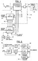
- Fig. 1 is an overall block diagram illustrating the invention.
- Fig. 2 is a block diagram of the PVT monitor circuit shown in Fig. 1.
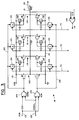
- Fig. 3 is a circuit diagram of the programmable output pad circuit shown in the block diagram of Fig. 1.
- Fig. 4 is a chart illustrating control outputs generated by the microprocessor of Fig. 1, in response to PVT readings and determined network electrical characteristics.
- a semiconductor chip 10 (shown dotted)includes a main circuit area 12 and a margin area 14. Within margin area 14, a plurality of input/output (I/O) pads 15 are positioned. Each pad 15 is connected to a programmable I/O circuit 16 which is, in turn, connected to a circuit in main circuit area 12. A PVT monitor circuit is positioned within margin area 14 and is connected to a microprocessor 20. Programmable I/O circuit 16 is also connected to microprocessor 20.
- Microprocessor 20 is provided with a read-only memory (ROM) 22 and a random access memory (RAM) 24. While microprocessor 20 is shown positioned off of chip 10, it could also be emplaced within main circuit area 12 of chip 10.
- ROM read-only memory
- RAM random access memory
- Chip 10 is mounted on a circuit carrier 25 and is connected thereto by a plurality of pins 28 (both schematically shown to illustrate the capacitive loading created thereby). Each pin 28 is connected through I/O pad 15 to programmable I/O circuit 16.
- Circuit carrier 25 may be a printed circuit board, a ceramic multi-layer circuit board, or other chip carrier. Pin 28 may also be connected to other circuit carrier connectors which may or may not be populated. Each circuit carrier 25 connected to pin 28 modifies the output impedance seen from pad 15 and, as a result, the load capacitance reflected into programmable I/O drive circuit 16.
- Microprocessor 20 is provided with a bidirectional output bus 30 which is, in turn, connected to the various circuit carriers. Microprocessor 20 at power-up, surveys signals from the circuit carriers populating the system and determines the circuit carrier configuration connected to each pad 15. As an alternate, microprocessor 20 may have the system configuration pre-programmed therein. Under such circumstances microprocessor 20 would only survey signals from included circuit carriers.
- ROM 22 stores a table which enables microprocessor 20 to convert the findings from the survey of circuit carriers to load capacitance values. From the derived load capacitances, microprocessor 20 then has part of the information required to enable the structuring of each programmable I/O circuit 16. The remaining portion of the information is supplied from PVT monitor 18. Details of PVT monitor 18 are shown in Fig. 2.
- Ring oscillator 50 is a 13-stage, oscillator whose frequency is, to a first order, dependent upon process, supply voltage and chip temperature parameters.
- Oscillator 50 is preferrably constructed of CMOS inverter gates.
- the output of ring oscillator 50 is applied to an input to a multiplexer 52.
- Another input to multiplexer 52 is the system clock, as received from input line 54.
- the output of multiplexer 52 is fed to a 4-bit counter 56 which, in turn, provides four outputs 58 indicative of its count.
- a four position latch 60 receives and stores, periodically, the outputs from counter 56 and manifests the stored values on output lines 62 (see also Fig. 1) to microprocessor 20.
- the 4-bit size of counter 56 is merely chosen as an example and other bit lengths are equally applicable.
- the system clock on input line 54 is also applied to a second multiplexer 64, along with a control SRT input 66 from microprocessor 20.
- the output of multiplexer 64 is applied to a latch and clear generator 66 whose outputs control 4-bit counter 56 and latch 60.
- Multiplexers 62, 64 and the SRT input are used for test purposes and are not directly relevant to this invention.
- Ring oscillator 50 is caused to oscillate (during a time that a PVT reading is required) by a control level on input 68 from microprocessor 20.
- Counter 56 begins a count of the oscillations emanating from oscillator 50.
- latch and clear generator 66 issues a signal which causes the count present in counter 56 to be latched into latch 60 and then resets counter 56. Because the system clock is crystal controlled and invariant, its use as a reference enables the oscillator count to be an accurate representation of PVT variations.
- the latched count appears on output lines 62 and provides a 4-bit indication of the number of oscillation cycles that have occurred between positive going system clock signals. That indication is representative of the combined PVT parameters present within chip 10.
- microprocessor 20 receives a 4-bit PVT value from PVT monitor 18 and has further derived the load capacitance of the network attached to terminal 28, it is able to provide signals to programmable I/O circuit 16 which adjust the output drive strength at output pin 28. Those signals are binary and are passed via output control lines 70, 72 and 74 to programmable I/O circuit 16. While three output control lines are shown, it is to be understood that this is merely exemplary and more control lines may be provided, one for each controllable stage within programmable I/O circuit 16. The details of programmable I/O circuit 16 are shown in Fig. 3.
- a signal input 100 provides an input level from a circuit within main circuit area 12.
- An output enable level OEN is applied to input terminal 102 to place the circuit into an output mode.
- the OEN level enables NAND and NOR gates 104 and 106, respectively, to respond to input signal transitions appearing on input line 100.
- the OEN level enables programmable I/O circuit 16 to exhibit a tri-state output characteristic - i.e., "0", "1" or high impedance. If the high impedance output is not required, the circuit can be configured to just produce "0" or "1" levels.
- a plurality of inverter output stages 108, 110, 112 and 114 are connected, in parallel, between a VDD bus 116 and a ground bus 118.
- Each inverter stage is comprised of a pair of complementary field effect transistors, connected source to drain and between VDD bus 116 and ground bus 118.
- An output line 120 interconnects each inverter's common source/drain interconnection to output pad 15.
- Output pad 15 is in turn connected to output pin 28, and from there to the circuit carrier network.
- Inverter 108 is not programmable and is always connected to output signal busses 126 and 128, (which, in turn, manifest the outputs from NAND and NOR gates 104 and 106, respectively).
- Inverters 110, 112 and 114 are programmable via the action of transmission gates 124, 130 and 132, respectively. More specifically, the gates of the upper and lower transistors in inverter 110 are connected through transmission gates 124, to output signal busses 126 and 128 respectively.
- transmission gates 130 and 132 interconnect the gates of the upper and lower transistors of inverters 112 and 114 to output signal buses 126 and 128.
- the controlling inputs for transmission gates 124, 130 and 132 are respectively derived from control inputs 70, 72 and 74 from microprocessor 20. Depending upon the logical levels applied to control inputs 70, 72 and 74, inverters 110, 112 and 114 will either be connected to or disconnected from output signal buses 126, 128.
- Additional transmission gates 124,' 130' and 132' connect the gates of the transistors in inverters 110, 112 and 114 to VDD and ground lines 116 and 128, respectively.
- Each of gates 124', 130' and 132' is fed through an inverter and evidences a complementary state to transmission gates 124, 130 and 132 respectively.
- Transmission gates 124', 130' and 132' when conductive, assure that the gates of the inverter transistors do not float and are tied to a supply bus.
- Control inputs 70, 72 and 74 together, manifest a 3-bit binary word whose value can range from 0 to 7 depending upon the applied levels.
- inverter stages 110, 112 and 114 which may be connected between output signal buses 126 and 128.
- Each inverter stage can impress upon output line 120; a high voltage value (VDD); a low voltage (ground); or a high impedance interface when both transistors are nonconductive.
- VDD high voltage value
- ground low voltage
- NOR gate 106 When OEN line 102 is active low and signal line 100 is active high, NAND gate 104 and NOR gate 106 will provide complementary output values to drive the transistors of a connected inverter.
- OEN line 102 is active low, outputs from NAND gate 104 and NOR gate 106 render connected inverter transistors into a nonconductive state.
- the transistors in inverters 110, 112 and 114 are sized to provide a binary progression of drive capability.
- the transistors in inverter 114 are designed to have a conduction channel which is four times larger than the transistors in inverter 110, and the transistors in inverter 112 are sized to have a conduction channel twice as large as the the transistors in inverter 110.
- the combination of binary sized conduction channels with binary control inputs provides a linear output progression of output drives on output line 120 with a progression of count values on control inputs 70, 72 and 74.
- Programmable I/O circuit 16 also includes an input function which is enabled by an IEN level applied to NOR circuit 140.
- the input circuit is not programmable and is not an important feature of this invention.
- a table (exemplary) is shown that is stored in ROM 22 (or in RAM 24) and provides digital values for control inputs 70, 72 and 74 of programmable I/O circuit 16.
- PVT readings vary from 0000 to 1111, with the lower binary values indicating a "slow" oscillator frequency and the higher binary values indicating a "fast” oscillator frequency.
- a slow oscillator frequency is indicative of one or more of the following: a high temperature leading to reduced transconductances; a low voltage from the VDD supply; a process variation that causes electron mobilities to be affected, etc.
- a fast oscillator frequency indicates the opposite.
- the horizontal axis of the table in Fig. 4 indicates pad load capacitances that are determined by microprocessor 20 in response to its survey of circuit carriers connected to output pin 28. Thus, certain combinations of circuit carriers will result in a large output capacitance, whereas other configurations will result in lower output capacitances.
- the table shown in Fig. 4 may be interpreted as follows. For a fast oscillator value (1111) and a low output load capacitance (e.g.. 70 - 80 pF), the table cause 0's to be output on control lines 70, 72 and 74 (e.g. low logical levels). The low levels on output lines 70, 72 and 74 cause switches 124, 130 and 132, respectively, to be in their nonconductive states. However, since inverter 108 is always connected to output signal buses 126 and 128, a minimum output drive current is provided to output pad 15.
- ground or supply bounce is an overshoot or ringing that occurs when fast rise or fall, large outputs are emplaced upon output conductor 120.
- Ground or supply bounce is related to the rate of change of gate signals to inverters 108, 110, 112 and 114. This effect is reduced in the circuit shown in Fig. 3 due to the fact that the gate capacitances of the transistors in inverters 110, 112 and 114 are increasingly larger with conduction channel size.
- the transistors in inverter 110 will be rendered conductive shortly before the transistors in inverter 112.
- transistors in inverter 112 will become conductive shortly before the transistors in inverter 114, all because of the different gate capacitance charge times through gates 124, 130 and 132 (all of which exhibit the same resistance). This effect will affect the signal rise time and reduce resulting ground bounce.
- microprocessor 20 can readjust each programmable I/O circuit in accordance with the then extant parameters.
Landscapes
- Physics & Mathematics (AREA)
- Engineering & Computer Science (AREA)
- Computer Hardware Design (AREA)
- Computing Systems (AREA)
- General Engineering & Computer Science (AREA)
- Mathematical Physics (AREA)
- Logic Circuits (AREA)
- Electronic Switches (AREA)
Applications Claiming Priority (2)
| Application Number | Priority Date | Filing Date | Title |
|---|---|---|---|
| US07/807,971 US5337254A (en) | 1991-12-16 | 1991-12-16 | Programmable integrated circuit output pad |
| US807971 | 1991-12-16 |
Publications (3)
| Publication Number | Publication Date |
|---|---|
| EP0547349A2 true EP0547349A2 (de) | 1993-06-23 |
| EP0547349A3 EP0547349A3 (de) | 1993-08-04 |
| EP0547349B1 EP0547349B1 (de) | 2000-12-27 |
Family
ID=25197556
Family Applications (1)
| Application Number | Title | Priority Date | Filing Date |
|---|---|---|---|
| EP92118747A Expired - Lifetime EP0547349B1 (de) | 1991-12-16 | 1992-11-02 | Integrierte Schaltung mit programmierbarem Ausgang |
Country Status (4)
| Country | Link |
|---|---|
| US (1) | US5337254A (de) |
| EP (1) | EP0547349B1 (de) |
| JP (1) | JP3425172B2 (de) |
| DE (1) | DE69231612T2 (de) |
Cited By (6)
| Publication number | Priority date | Publication date | Assignee | Title |
|---|---|---|---|---|
| WO1998036497A1 (en) * | 1997-02-18 | 1998-08-20 | Rambus, Inc. | Bus driver circuit including a slew rate indicator circuit having a series of delay elements |
| US5959481A (en) | 1997-02-18 | 1999-09-28 | Rambus Inc. | Bus driver circuit including a slew rate indicator circuit having a one shot circuit |
| EP0714167B1 (de) * | 1994-11-22 | 2002-02-20 | Micronas GmbH | Digitale Treiberschaltung für eine integrierte Schaltung |
| GB2375446A (en) * | 2001-03-20 | 2002-11-13 | Hewlett Packard Co | Controlled impedance driver receiving a combination binary and thermometer code |
| US9251913B2 (en) | 2011-06-09 | 2016-02-02 | International Business Machines Corporation | Infrastructure for performance based chip-to-chip stacking |
| WO2019022825A3 (en) * | 2017-07-28 | 2019-05-16 | Qualcomm Incorporated | Voltage histogram generation |
Families Citing this family (31)
| Publication number | Priority date | Publication date | Assignee | Title |
|---|---|---|---|---|
| US5739714A (en) * | 1995-10-24 | 1998-04-14 | Lucent Technologies, Inc. | Apparatus for controlling ground bounce |
| US5844928A (en) * | 1996-02-27 | 1998-12-01 | Lucent Technologies, Inc. | Laser driver with temperature sensor on an integrated circuit |
| US6085033A (en) * | 1997-06-25 | 2000-07-04 | Sun Microsystems, Inc. | Method for determining bit element values for driver impedance control |
| US6363505B1 (en) * | 1997-11-14 | 2002-03-26 | Altera Corporation | Programmable control circuit for grounding unused outputs |
| US6496037B1 (en) * | 2000-06-06 | 2002-12-17 | International Business Machines Corporation | Automatic off-chip driver adjustment based on load characteristics |
| WO2001096893A1 (en) * | 2000-06-16 | 2001-12-20 | Transmeta Corporation | Apparatus for controlling semiconductor chip characteristics |
| US6335638B1 (en) | 2000-06-29 | 2002-01-01 | Pericom Semiconductor Corp. | Triple-slope clock driver for reduced EMI |
| US6864706B1 (en) * | 2000-07-20 | 2005-03-08 | Silicon Graphics, Inc. | GTL+Driver |
| US7849332B1 (en) | 2002-11-14 | 2010-12-07 | Nvidia Corporation | Processor voltage adjustment system and method |
| US7882369B1 (en) | 2002-11-14 | 2011-02-01 | Nvidia Corporation | Processor performance adjustment system and method |
| US7886164B1 (en) | 2002-11-14 | 2011-02-08 | Nvidia Corporation | Processor temperature adjustment system and method |
| US20050028020A1 (en) * | 2003-07-28 | 2005-02-03 | Ryan Zarrieff | Spread spectrum clocking for data transfer bus loading |
| JP4610919B2 (ja) * | 2004-03-29 | 2011-01-12 | ルネサスエレクトロニクス株式会社 | 半導体集積回路装置 |
| US7330080B1 (en) * | 2004-11-04 | 2008-02-12 | Transmeta Corporation | Ring based impedance control of an output driver |
| US7157932B2 (en) * | 2004-11-30 | 2007-01-02 | Agere Systems Inc. | Adjusting settings of an I/O circuit for process, voltage, and/or temperature variations |
| US7348857B1 (en) * | 2005-02-28 | 2008-03-25 | Marvell Semiconductor Israel Ltd. | Monitoring and compensating for real time local circuit speed in an integrated circuit |
| US7739531B1 (en) * | 2005-03-04 | 2010-06-15 | Nvidia Corporation | Dynamic voltage scaling |
| US7327167B2 (en) * | 2005-04-28 | 2008-02-05 | Silicon Graphics, Inc. | Anticipatory programmable interface pre-driver |
| JP2007184809A (ja) * | 2006-01-10 | 2007-07-19 | Epson Toyocom Corp | 発振装置 |
| US9134782B2 (en) | 2007-05-07 | 2015-09-15 | Nvidia Corporation | Maintaining optimum voltage supply to match performance of an integrated circuit |
| WO2009058141A1 (en) * | 2007-10-31 | 2009-05-07 | Agere Systems Inc. | Compensation techniques for reducing power comsumption in digital circuitry |
| US7812639B2 (en) * | 2007-12-31 | 2010-10-12 | Sandisk Corporation | Extending drive capability in integrated circuits utilizing programmable-voltage output circuits |
| US8370663B2 (en) * | 2008-02-11 | 2013-02-05 | Nvidia Corporation | Power management with dynamic frequency adjustments |
| US8001434B1 (en) | 2008-04-14 | 2011-08-16 | Netlist, Inc. | Memory board with self-testing capability |
| US8154901B1 (en) | 2008-04-14 | 2012-04-10 | Netlist, Inc. | Circuit providing load isolation and noise reduction |
| JP2010178262A (ja) * | 2009-02-02 | 2010-08-12 | Fujitsu Semiconductor Ltd | ドライバストレングス調整回路、半導体集積回路、及びドライバストレングスの調整方法 |
| US9256265B2 (en) | 2009-12-30 | 2016-02-09 | Nvidia Corporation | Method and system for artificially and dynamically limiting the framerate of a graphics processing unit |
| US9830889B2 (en) | 2009-12-31 | 2017-11-28 | Nvidia Corporation | Methods and system for artifically and dynamically limiting the display resolution of an application |
| US8839006B2 (en) | 2010-05-28 | 2014-09-16 | Nvidia Corporation | Power consumption reduction systems and methods |
| US9928194B2 (en) | 2015-11-30 | 2018-03-27 | Allegro Microsystems, Llc | Non-linear transmit biasing for a serial bus transmitter |
| US9621140B1 (en) | 2016-01-15 | 2017-04-11 | Allegro Microsystems, Llc | Electronic circuit for driving an output current signal and method of driving the output current signal from the electronic circuit to achieve an altered transition of the output current signal |
Citations (5)
| Publication number | Priority date | Publication date | Assignee | Title |
|---|---|---|---|---|
| EP0184875A1 (de) * | 1984-12-05 | 1986-06-18 | Koninklijke Philips Electronics N.V. | Adaptives elektronisches Pufferverstärkersystem |
| EP0253914A1 (de) * | 1986-07-23 | 1988-01-27 | Deutsche ITT Industries GmbH | Isolierschicht-Feldeffekttransistor-Gegentakttreiberstufe mit Kompensierung von Betriebsparameterschwankungen und Fertigungsstreuungen |
| EP0463316A1 (de) * | 1990-06-07 | 1992-01-02 | International Business Machines Corporation | Selbsteinstellender Treiber für Impedanzanpassung |
| EP0482392A2 (de) * | 1990-10-26 | 1992-04-29 | Alcatel SEL Aktiengesellschaft | Schaltungsanordnung zur Bereitstellung eines Ausgangsstromes für einen Datentreiber |
| EP0520687A1 (de) * | 1991-06-28 | 1992-12-30 | AT&T Corp. | Digital gesteuerte Bauelement-Grössenbemessung |
Family Cites Families (14)
| Publication number | Priority date | Publication date | Assignee | Title |
|---|---|---|---|---|
| JPS5772429A (en) * | 1980-10-22 | 1982-05-06 | Toshiba Corp | Semiconductor integrated circuit device |
| US4383216A (en) * | 1981-01-29 | 1983-05-10 | International Business Machines Corporation | AC Measurement means for use with power control means for eliminating circuit to circuit delay differences |
| US4494021A (en) * | 1982-08-30 | 1985-01-15 | Xerox Corporation | Self-calibrated clock and timing signal generator for MOS/VLSI circuitry |
| US4684897A (en) * | 1984-01-03 | 1987-08-04 | Raytheon Company | Frequency correction apparatus |
| US4641048A (en) * | 1984-08-24 | 1987-02-03 | Tektronix, Inc. | Digital integrated circuit propagation delay time controller |
| US4623805A (en) * | 1984-08-29 | 1986-11-18 | Burroughs Corporation | Automatic signal delay adjustment apparatus |
| US5086238A (en) * | 1985-07-22 | 1992-02-04 | Hitachi, Ltd. | Semiconductor supply incorporating internal power supply for compensating for deviation in operating condition and fabrication process conditions |
| US4691124A (en) * | 1986-05-16 | 1987-09-01 | Motorola, Inc. | Self-compensating, maximum speed integrated circuit |
| EP0264470B1 (de) * | 1986-10-21 | 1991-03-06 | International Business Machines Corporation | Verfahren zur digitalen Regelung der Flankensteilheit der Ausgangssignale von Leistungsverstärkern der für einen Computer bestimmten Halbleiterchips mit hochintegrierten Schaltungen |
| US4818901A (en) * | 1987-07-20 | 1989-04-04 | Harris Corporation | Controlled switching CMOS output buffer |
| US4939389A (en) * | 1988-09-02 | 1990-07-03 | International Business Machines Corporation | VLSI performance compensation for off-chip drivers and clock generation |
| US5198759A (en) * | 1990-11-27 | 1993-03-30 | Alcatel N.V. | Test apparatus and method for testing digital system |
| US5198758A (en) * | 1991-09-23 | 1993-03-30 | Digital Equipment Corp. | Method and apparatus for complete functional testing of a complex signal path of a semiconductor chip |
| US5272390A (en) * | 1991-09-23 | 1993-12-21 | Digital Equipment Corporation | Method and apparatus for clock skew reduction through absolute delay regulation |
-
1991
- 1991-12-16 US US07/807,971 patent/US5337254A/en not_active Expired - Lifetime
-
1992
- 1992-11-02 EP EP92118747A patent/EP0547349B1/de not_active Expired - Lifetime
- 1992-11-02 DE DE69231612T patent/DE69231612T2/de not_active Expired - Fee Related
- 1992-12-16 JP JP33592192A patent/JP3425172B2/ja not_active Expired - Fee Related
Patent Citations (5)
| Publication number | Priority date | Publication date | Assignee | Title |
|---|---|---|---|---|
| EP0184875A1 (de) * | 1984-12-05 | 1986-06-18 | Koninklijke Philips Electronics N.V. | Adaptives elektronisches Pufferverstärkersystem |
| EP0253914A1 (de) * | 1986-07-23 | 1988-01-27 | Deutsche ITT Industries GmbH | Isolierschicht-Feldeffekttransistor-Gegentakttreiberstufe mit Kompensierung von Betriebsparameterschwankungen und Fertigungsstreuungen |
| EP0463316A1 (de) * | 1990-06-07 | 1992-01-02 | International Business Machines Corporation | Selbsteinstellender Treiber für Impedanzanpassung |
| EP0482392A2 (de) * | 1990-10-26 | 1992-04-29 | Alcatel SEL Aktiengesellschaft | Schaltungsanordnung zur Bereitstellung eines Ausgangsstromes für einen Datentreiber |
| EP0520687A1 (de) * | 1991-06-28 | 1992-12-30 | AT&T Corp. | Digital gesteuerte Bauelement-Grössenbemessung |
Non-Patent Citations (1)
| Title |
|---|
| IBM TECHNICAL DISCLOSURE BULLETIN. vol. 30, no. 7, December 1987, NEW YORK US pages 23 - 25 'auto programming lumped off-chip drivers' * |
Cited By (6)
| Publication number | Priority date | Publication date | Assignee | Title |
|---|---|---|---|---|
| EP0714167B1 (de) * | 1994-11-22 | 2002-02-20 | Micronas GmbH | Digitale Treiberschaltung für eine integrierte Schaltung |
| WO1998036497A1 (en) * | 1997-02-18 | 1998-08-20 | Rambus, Inc. | Bus driver circuit including a slew rate indicator circuit having a series of delay elements |
| US5959481A (en) | 1997-02-18 | 1999-09-28 | Rambus Inc. | Bus driver circuit including a slew rate indicator circuit having a one shot circuit |
| GB2375446A (en) * | 2001-03-20 | 2002-11-13 | Hewlett Packard Co | Controlled impedance driver receiving a combination binary and thermometer code |
| US9251913B2 (en) | 2011-06-09 | 2016-02-02 | International Business Machines Corporation | Infrastructure for performance based chip-to-chip stacking |
| WO2019022825A3 (en) * | 2017-07-28 | 2019-05-16 | Qualcomm Incorporated | Voltage histogram generation |
Also Published As
| Publication number | Publication date |
|---|---|
| US5337254A (en) | 1994-08-09 |
| DE69231612D1 (de) | 2001-02-01 |
| EP0547349A3 (de) | 1993-08-04 |
| JP3425172B2 (ja) | 2003-07-07 |
| EP0547349B1 (de) | 2000-12-27 |
| JPH0690160A (ja) | 1994-03-29 |
| DE69231612T2 (de) | 2001-05-03 |
Similar Documents
| Publication | Publication Date | Title |
|---|---|---|
| US5337254A (en) | Programmable integrated circuit output pad | |
| US5877634A (en) | CMOS buffer with controlled slew rate | |
| US9411767B2 (en) | Flash controller to provide a value that represents a parameter to a flash memory | |
| US5568068A (en) | Buffer circuit for regulating driving current | |
| EP0883248B1 (de) | Integrierte Halbleiterschaltung mit Eingangs/Ausgangschnittstelle geeignet für niedrige Amplituden | |
| KR100875675B1 (ko) | 임피던스 조정된 의사 오픈 드레인 출력 드라이버 | |
| KR100655083B1 (ko) | 반도체 장치에서의 임피던스 콘트롤 회로 및 임피던스콘트롤 방법 | |
| KR100318685B1 (ko) | 프로그래머블임피던스콘트롤회로 | |
| US7268602B2 (en) | Method and apparatus for accommodating delay variations among multiple signals | |
| GB2317515A (en) | Binary data link with reduced termination resistor dissipation | |
| US6987407B2 (en) | Delay locked loops having delay time compensation and methods for compensating for delay time of the delay locked loops | |
| US6941526B2 (en) | Low power buffer implementation | |
| US6781428B2 (en) | Input circuit with switched reference signals | |
| US20040080336A1 (en) | Output buffer apparatus capable of adjusting output impedance in synchronization with data signal | |
| US5852372A (en) | Apparatus and method for signal handling on GTL-type buses | |
| US7339399B2 (en) | Anti-noise input/output impedance control of semiconductor circuit with reduced circuit size | |
| US5686851A (en) | Variable delay circuit | |
| JP3460802B2 (ja) | 半導体装置 | |
| US11742856B2 (en) | Digital buffer device with self-calibration | |
| JP2500775B2 (ja) | 半導体集積回路 | |
| US20040225976A1 (en) | Glitch free programmable delay line for edge sensitive design | |
| KR960005017Y1 (ko) | 데이타 출력버퍼 | |
| KR20080072982A (ko) | 듀얼 파워 차동증폭기 회로 |
Legal Events
| Date | Code | Title | Description |
|---|---|---|---|
| PUAI | Public reference made under article 153(3) epc to a published international application that has entered the european phase |
Free format text: ORIGINAL CODE: 0009012 |
|
| PUAL | Search report despatched |
Free format text: ORIGINAL CODE: 0009013 |
|
| AK | Designated contracting states |
Kind code of ref document: A2 Designated state(s): DE FR GB IT |
|
| AK | Designated contracting states |
Kind code of ref document: A3 Designated state(s): DE FR GB IT |
|
| 17P | Request for examination filed |
Effective date: 19940126 |
|
| 17Q | First examination report despatched |
Effective date: 19960208 |
|
| GRAG | Despatch of communication of intention to grant |
Free format text: ORIGINAL CODE: EPIDOS AGRA |
|
| GRAG | Despatch of communication of intention to grant |
Free format text: ORIGINAL CODE: EPIDOS AGRA |
|
| GRAH | Despatch of communication of intention to grant a patent |
Free format text: ORIGINAL CODE: EPIDOS IGRA |
|
| GRAH | Despatch of communication of intention to grant a patent |
Free format text: ORIGINAL CODE: EPIDOS IGRA |
|
| GRAA | (expected) grant |
Free format text: ORIGINAL CODE: 0009210 |
|
| AK | Designated contracting states |
Kind code of ref document: B1 Designated state(s): DE FR GB IT |
|
| REF | Corresponds to: |
Ref document number: 69231612 Country of ref document: DE Date of ref document: 20010201 |
|
| ET | Fr: translation filed | ||
| ITF | It: translation for a ep patent filed | ||
| RAP2 | Party data changed (patent owner data changed or rights of a patent transferred) |
Owner name: HEWLETT-PACKARD COMPANY, A DELAWARE CORPORATION |
|
| PLBE | No opposition filed within time limit |
Free format text: ORIGINAL CODE: 0009261 |
|
| STAA | Information on the status of an ep patent application or granted ep patent |
Free format text: STATUS: NO OPPOSITION FILED WITHIN TIME LIMIT |
|
| 26N | No opposition filed | ||
| REG | Reference to a national code |
Ref country code: GB Ref legal event code: IF02 |
|
| REG | Reference to a national code |
Ref country code: GB Ref legal event code: 732E |
|
| REG | Reference to a national code |
Ref country code: FR Ref legal event code: TP |
|
| PGFP | Annual fee paid to national office [announced via postgrant information from national office to epo] |
Ref country code: IT Payment date: 20061130 Year of fee payment: 15 |
|
| PGFP | Annual fee paid to national office [announced via postgrant information from national office to epo] |
Ref country code: GB Payment date: 20070125 Year of fee payment: 15 |
|
| PGFP | Annual fee paid to national office [announced via postgrant information from national office to epo] |
Ref country code: DE Payment date: 20070228 Year of fee payment: 15 |
|
| PGFP | Annual fee paid to national office [announced via postgrant information from national office to epo] |
Ref country code: FR Payment date: 20070207 Year of fee payment: 15 |
|
| GBPC | Gb: european patent ceased through non-payment of renewal fee |
Effective date: 20071102 |
|
| PG25 | Lapsed in a contracting state [announced via postgrant information from national office to epo] |
Ref country code: DE Free format text: LAPSE BECAUSE OF NON-PAYMENT OF DUE FEES Effective date: 20080603 |
|
| REG | Reference to a national code |
Ref country code: FR Ref legal event code: ST Effective date: 20080930 |
|
| PG25 | Lapsed in a contracting state [announced via postgrant information from national office to epo] |
Ref country code: GB Free format text: LAPSE BECAUSE OF NON-PAYMENT OF DUE FEES Effective date: 20071102 |
|
| PG25 | Lapsed in a contracting state [announced via postgrant information from national office to epo] |
Ref country code: FR Free format text: LAPSE BECAUSE OF NON-PAYMENT OF DUE FEES Effective date: 20071130 |
|
| PG25 | Lapsed in a contracting state [announced via postgrant information from national office to epo] |
Ref country code: IT Free format text: LAPSE BECAUSE OF NON-PAYMENT OF DUE FEES Effective date: 20071102 |