EP0545577B1 - Display system and method - Google Patents
Display system and method Download PDFInfo
- Publication number
- EP0545577B1 EP0545577B1 EP92310528A EP92310528A EP0545577B1 EP 0545577 B1 EP0545577 B1 EP 0545577B1 EP 92310528 A EP92310528 A EP 92310528A EP 92310528 A EP92310528 A EP 92310528A EP 0545577 B1 EP0545577 B1 EP 0545577B1
- Authority
- EP
- European Patent Office
- Prior art keywords
- modification values
- line
- bits
- bit signals
- values
- Prior art date
- Legal status (The legal status is an assumption and is not a legal conclusion. Google has not performed a legal analysis and makes no representation as to the accuracy of the status listed.)
- Expired - Lifetime
Links
Images


Classifications
-
- G—PHYSICS
- G06—COMPUTING; CALCULATING OR COUNTING
- G06F—ELECTRIC DIGITAL DATA PROCESSING
- G06F3/00—Input arrangements for transferring data to be processed into a form capable of being handled by the computer; Output arrangements for transferring data from processing unit to output unit, e.g. interface arrangements
- G06F3/14—Digital output to display device ; Cooperation and interconnection of the display device with other functional units
- G06F3/153—Digital output to display device ; Cooperation and interconnection of the display device with other functional units using cathode-ray tubes
-
- G—PHYSICS
- G06—COMPUTING; CALCULATING OR COUNTING
- G06F—ELECTRIC DIGITAL DATA PROCESSING
- G06F3/00—Input arrangements for transferring data to be processed into a form capable of being handled by the computer; Output arrangements for transferring data from processing unit to output unit, e.g. interface arrangements
- G06F3/14—Digital output to display device ; Cooperation and interconnection of the display device with other functional units
- G06F3/147—Digital output to display device ; Cooperation and interconnection of the display device with other functional units using display panels
- G06F3/1475—Digital output to display device ; Cooperation and interconnection of the display device with other functional units using display panels with conversion of CRT control signals to flat panel control signals, e.g. adapting the palette memory
-
- G—PHYSICS
- G09—EDUCATION; CRYPTOGRAPHY; DISPLAY; ADVERTISING; SEALS
- G09G—ARRANGEMENTS OR CIRCUITS FOR CONTROL OF INDICATING DEVICES USING STATIC MEANS TO PRESENT VARIABLE INFORMATION
- G09G3/00—Control arrangements or circuits, of interest only in connection with visual indicators other than cathode-ray tubes
- G09G3/20—Control arrangements or circuits, of interest only in connection with visual indicators other than cathode-ray tubes for presentation of an assembly of a number of characters, e.g. a page, by composing the assembly by combination of individual elements arranged in a matrix no fixed position being assigned to or needed to be assigned to the individual characters or partial characters
- G09G3/34—Control arrangements or circuits, of interest only in connection with visual indicators other than cathode-ray tubes for presentation of an assembly of a number of characters, e.g. a page, by composing the assembly by combination of individual elements arranged in a matrix no fixed position being assigned to or needed to be assigned to the individual characters or partial characters by control of light from an independent source
- G09G3/36—Control arrangements or circuits, of interest only in connection with visual indicators other than cathode-ray tubes for presentation of an assembly of a number of characters, e.g. a page, by composing the assembly by combination of individual elements arranged in a matrix no fixed position being assigned to or needed to be assigned to the individual characters or partial characters by control of light from an independent source using liquid crystals
- G09G3/3611—Control of matrices with row and column drivers
-
- G—PHYSICS
- G09—EDUCATION; CRYPTOGRAPHY; DISPLAY; ADVERTISING; SEALS
- G09G—ARRANGEMENTS OR CIRCUITS FOR CONTROL OF INDICATING DEVICES USING STATIC MEANS TO PRESENT VARIABLE INFORMATION
- G09G2340/00—Aspects of display data processing
- G09G2340/04—Changes in size, position or resolution of an image
- G09G2340/0407—Resolution change, inclusive of the use of different resolutions for different screen areas
- G09G2340/0414—Vertical resolution change
-
- G—PHYSICS
- G09—EDUCATION; CRYPTOGRAPHY; DISPLAY; ADVERTISING; SEALS
- G09G—ARRANGEMENTS OR CIRCUITS FOR CONTROL OF INDICATING DEVICES USING STATIC MEANS TO PRESENT VARIABLE INFORMATION
- G09G2340/00—Aspects of display data processing
- G09G2340/04—Changes in size, position or resolution of an image
- G09G2340/0407—Resolution change, inclusive of the use of different resolutions for different screen areas
- G09G2340/0421—Horizontal resolution change
-
- G—PHYSICS
- G09—EDUCATION; CRYPTOGRAPHY; DISPLAY; ADVERTISING; SEALS
- G09G—ARRANGEMENTS OR CIRCUITS FOR CONTROL OF INDICATING DEVICES USING STATIC MEANS TO PRESENT VARIABLE INFORMATION
- G09G2340/00—Aspects of display data processing
- G09G2340/04—Changes in size, position or resolution of an image
- G09G2340/0442—Handling or displaying different aspect ratios, or changing the aspect ratio
-
- G—PHYSICS
- G09—EDUCATION; CRYPTOGRAPHY; DISPLAY; ADVERTISING; SEALS
- G09G—ARRANGEMENTS OR CIRCUITS FOR CONTROL OF INDICATING DEVICES USING STATIC MEANS TO PRESENT VARIABLE INFORMATION
- G09G3/00—Control arrangements or circuits, of interest only in connection with visual indicators other than cathode-ray tubes
- G09G3/20—Control arrangements or circuits, of interest only in connection with visual indicators other than cathode-ray tubes for presentation of an assembly of a number of characters, e.g. a page, by composing the assembly by combination of individual elements arranged in a matrix no fixed position being assigned to or needed to be assigned to the individual characters or partial characters
- G09G3/2007—Display of intermediate tones
- G09G3/2044—Display of intermediate tones using dithering
- G09G3/2051—Display of intermediate tones using dithering with use of a spatial dither pattern
Description
- The present invention relates to a display system for converting an N bit signal representing 2N gray levels (N being an integer larger than or equal to 2), to an M bit signal representing 2M gray levels (M being an integer satisfying N>M≥1).
- US Patent 5059962 describes a display system comprising a Cathode Ray Tube (CRT) display device connected to a personal computer via a digital to analog convertor and a Liquid Crystal Display (LCD) device connected to the computer via a LCD controller. The two devices can display different ranges of gray levels. Specifically, the CRT display device can display 64 gray levels, but the LCD device can display only 16 gray levels. The personal computer supplies a 6 bit signal for each picture element (pel). The 6 bit signal represents the 64 gray levels of the CRT display device. To display 64 gray levels on the LCD device, LCD controller generates four 4 bit signals in response to each 6 bit signal. The 4 bit signal represents the 16 gray levels displayed by one pel of the LCD device. Four pels of the LCD device are used to display the four 4 bit signals. Thus, if the picture supplied by the
computer 20 has 320x200 pels, the CRT display device displays a picture having 320x200 pels and the LCD device displays a picture having 640x400 pels. - The aspect ratio of the CRT display device is A:B. The pitch between adjacent horizontal scanning lines in the CRT display device is determined by a vertical scanning signal. The scanning signal is controlled, by values of capacitors, coils, and resistors in a deflection circuit, to repeatedly display the same horizontal pels on two adjacent horizontal scan lines. In other words, 200 x 2 = 400 horizontal scan lines are displayed in dimension B of the CRT display device. The spacing between pels in the LCD device is determined during fabrication of the LCD panel. In general, the aspect ratio C:D of the LCD device differs from the aspect ratio A:B of the CRT display device. Generally, the image displayed on the LCD device is compressed or stretched vertically with respect to the image displayed on the CRT display device.
- In accordance with the present invention there is provided a display system for converting N bit signals each, representing 2N grey scale levels, to M bit signals representing 2M grey levels, where N is an integer larger than or equal to 2 and M is an integer satisfying N>M≥1, the system comprising: means for separating each of the N bit signals into higher order M bits and N-M bits; 2N-M tables each storing a distinctive set of PxQ modification values satisfying PxQ≥2N-M: means for selecting one of the tables as a function of the N-M bits; means for detecting a difference between a first set of modification values and a second set of modification values of the selected table, means for exchanging the first set of modification values and the second set of modification values to generate a modified table from the selected table; means for adding the M bits of one N bit signal and each of the modification values of one of said modified or the selected table to generate a set of PxQ M bit signals; and means for supplying the set of M bit signals to a display device of 2M grey levels.
- This advantageously permits the addition of pel lines to the picture displayed on the LCD device to bring the aspect ratio of the LCD device into line with that of the CRT device without introducing inconsistent grey levels into the picture.
- The display device preferably receives the first and second sets of PxQ M bit signals to display them on Q image lines and the same image as that of the Qth image line on one additional line.
- Viewing the present invention from a second aspect, there is provided a method for converting N bit signals each, representing 2N grey levels, to M bit signals representing 2M grey levels, where N is an integer larger than or equal to 2 and M is an integer satisfying N>M≥1, said method comprising the steps of: separating each of said N bit signals into higher M bits and lower N-M bits; creating 2N-M tables each of which stores a distinct set of PxQ modification values satisfying PxQ≥2N-M; selecting one of said tables using said N-M bits; conditionally detecting unequality between first set of modification values and second set of modification values of said selected table; conditionally exchanging said first set of modification values and said second set of modification values to generated a modified table from said selected table; conditionally adding said M bits of one N bit signal and each of the modification values of one of said modified or said selected table to generate a set of PxQ M bit signals; and supplying said set of M bit signals to a display device of 2M grey levels.
- Preferred embodiments of the present invention will now be described with reference to the accompanying drawings, in which:
- Figure 1 is a block diagram of a display system of the present invention;
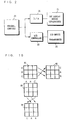
- Figure 2 is a block diagram of a conventional display system;
- Figure 3 shows the number of horizontal and vertical pels and aspect ratio of various display devices;
- Figure 4 is a flow chart of an embodiment of the present invention.
- Figures 5, 6 and 7 are pel patterns generated by the display system of the present invention;
- Figure 8 is a flow chart of another embodiment of the present invention;
- Figure 9 is a pel pattern generated in accordance with the flow chart shown in Figure 8;
- Figure 10 is an example of an alternate table; and
- Figures 11, 12, 13 and 14 show pel patterns generated by a display system of the prior art and in accordance with the present invention.
-
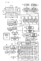
- Referring to Figure 2, an example of a conventional display system comprises a
CRT display device 21 and anLCD display device 25 both for displaying data produced by apersonal computer 20. The video output ofcomputer 20 is connected toCRT device 21 andLCD device 25 through a digital-analog converter 22 and aLCD controller 23, respectively.CRT device 21 displays 64 gray levels andLCD device 25 displays 16 gray levels.Computer 20 supplies a 6 bit signal for each picture element. The 6 bit signal represents the 64 gray levels of theCRT display device 25. To display the 64 gray levels onLCD device 25,LCD controller 23 generates four 4 bit signals in response to each 6 bit signal. The 4 bit signal represents the 16 gray levels displayable by one pel ofLCD device 25. Four pels ofLCD device 25 are used to display the four 4 bit signals. Thus, referring to Figure 3, if the picture supplied bycomputer 20 has 320x200 pels,CRT device 21 displays a picture having 320x200 pels andLCD device 25 displays a picture having has 640x400 dots. - Referring to Figure 1,
blocks LCD controller 23 are described in detail in the aforementioned US Patent 5059962, the contents of which is included herein in full. What follows is a brief description ofcontroller 23 in operation. - It will be assumed for the purpose of description that
control device 12 generates 6 bit gray level signal 101010 (decimal value 42) which is stored inregister 1.Control device 12 then loads the most significant 4 bits, M bits (1010), of the 6 bit signal into the least significant 4 bit positions ofregister 4 throughline 2. The most significant 2 bit positions ofregister 4 are always 00. The reason for concatenating the most significant 2 bits inregister 4 will be described below.Control device 12, online 3, supplies the least significant 2 bits, N-M bits, of the 6 bit signal 101010 as an address to select one of Tables 5, 6, 7 and 8. Tables 5, 6, 7, and 8 are known as dither matrices. The number of tables used is determined by 2N-M. Thus, 4 tables are prepared. The least significant 2 bits are represented by x and y in Figure 1. N is an integer larger than or equal to 2 and M is an integer satisfying N>M≥1. Since x=1 and y=0, Table 7 is selected. Each table stores 4 modification values, PxQ, satisfying PxQ≥2N-M. Each set of modification values corresponds to the 4 pels of each one ofareas LCD device 25. The modification values are represented in Figure 1 by decimal values, but as 0 corresponds to thebinary value 00000 and 1 corresponds to the binary value 00001, these binary values are actually stored in the tables. The modification value can be any value in the range from +15 to -15. The range +3 to -3 is however preferred for fidelity. The modification value has 5 bits representing +15 to -15. A negative value is represented by the complement of 2. A single most significant bit is concatenated to the 5 bits from the table by a sign extension. For example, where the modification value is +1, 00001 is stored in the table and 0 is concatenated to the 00001 by the sign extension. Thus, the input to adder 9 from the table is 000001. Where the modification value in the table is -1, 11111 is stored in the table, and 1 is concatenated to the 11111 by the sign extension. Thus, 111111 is supplied to adder 9. Since the input to adder 9 from the tables is 6 bits, the input fromregister 4 is also made to be 6 bits. Thus, the 2 mostsignificant bits 00 are concatenated inregister 4. - To generate a gray level signal for pel (0,0) of
area 14A ofLCD device 25,control device 12 first concatenates bit 0 to the upper left modification value 00000 in Table 7, and supplies 000000 to adder 9. Next,control device 12 activates adder 9 to add inputs from the table andregister 4. In other words, 000000 representing the upperleft modification value 0 in Table 7 is added to 001010 (2+M bits) to generate 001010.Control device 12transfers 001010 from adder 9 todiscrimination device 10.Discrimination device 10 generates a signal on the output line as a function of the total value received from adder 9.Device 10 generates a signal corresponding to 15 (binary value 1111) on the output line if the total value is larger than 15, generates 0 (binary value 0000) on the output line if the total value is less than 0 (negative), and supplies the lower 4 bits of the total value on the output line if the total value satisfies 15 ≥ total value ≥ 0. To perform the discrimination, the most significant 2 bits of the total value are tested. When the most significant bit is 1, the total value is negative. When the most significant 2 bits are 01, the total value is larger than 15, and when the most significant 2 bits are 00, the relation 15total value 0 is satisfied. In the case of the upper left modification value in Table 7, the total value is 001010. Thus, the 4 bits 1010 are supplied toLCD device 25 as the gray level signal for pel (0,0) inarea 14A. A gray level of 10 (i.e. binary value 1010) is therefore displayed at pel (0,0) ofdevice 25. - To generate a gray level signal for pel (1,0) in
area 14A ofdevice 25,control device 12 reads the upper right modification value 1 (binary value 00001) in table 7, converts it to the 6 bits 000001 by the sign extension, supplies those 6 bits to adder 9, and supplies the 6bits 001010 in 2+M register 4 to adder 9. Next, both of these values are added. The total value is 001011 and satisfies 15total value 0. Thus, the bits 1011 are supplied toLCD device 25 as the gray level signal for pel (1,0) inarea 14A. A gray level of 11 (binary value 1011) is therefore displayed at pel (1,0) ofdisplay device 25. -
Control device 12 performs the level conversion operation for the second pel (1,0) inpel line 0 ofCRT device 21 in the same manner. The gray level signals for pels (2,0) and (3,0) inarea 14B of theLCD device 25 are generated and these pels are displayed. Similarly, the third and subsequent pels inpel line 0 ofCRT device 21 can be converted, and the two pels inarea 14C and the subsequent areas ofLCD device 25 can be displayed. In this manner, the same image can be displayed on bothdevices CRT device 21 differs from those ofLCD device 25. As desired, both devices may be operated simultaneously or individually. - The gray level signals for pels of
line 1 ofLCD device 25 are generated in the same manner. Now, however, the lowerleft modification value 0 and lower right modification value -1 are used to generate the gray level signals for pels (0,1) and (1,1) respectively. - Referring to Figure 3, the aspect ratio of
CRT device 21 is A:B. The pitch between adjacent horizontal scanning lines onCRT device 21 is determined by a vertical scan signal. The scan signal is controlled, by values of capacitors, coils, and resistors in a deflection circuit, to repeatedly display the same horizontal pels on two adjacent horizontal scan lines. In other words, 200 x 2 = 400 horizontal scan lines are displayed in dimension B ofCRT device 21. The spacing between pels ofLCD device 25 is determined during fabrication of the LCD panel. Conventionally, the aspect ratio C:D ofLCD device 25 differs from the aspect ratio A:B ofCRT device 21. Usually, the picture produced byLCD device 25 is compressed or stretched vertically with respect to the picture displayed onCRT device 21. - In an example of a display system of the present invention,
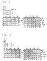
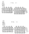
LCD device 25 has 640 horizontal pels and 480 vertical pels to display a picture of the same aspect ratio as that of CRT device 21 (A:B = E:F). The pel spacing of the 640X480 pel LCD device is equal to that of the conventional 640x400 pel LCD device. To realise A:B = E:F, one horizontal picture line is inserted every five horizontal picture lines. However, if the same picture information as that on the preceding image line is repeatedly displayed on the inserted line, the conventional gray level setting algorithm described above can produce visible mismatches between adjacent lines. - Figures 11 to 14 show the effect of the additional lines on the picture. In Figures 11 to 14, the insets are the 2x2 dither matrix tables 5-8 in Figure 1. The leftmost patterns show pels of the 640X400 LCD device generated conventionally as described in the aforementioned US Patent 5059962. The rightmost patterns show pels for the 640X480 pel LCD device generated by inserting additional lines in accordance with the present invention. Although the sum of the value (M bits) and the modification value of the tables is displayed in each pel of
LCD device 25, only the modification values are shown in Figures 11-14, since the value (M pels) is effectively a constant. Referring to Figure 1, Tables 5, 6, 7 and 8 of 2x2 pels, as mentioned earlier, are the dither matrices for the four gray levels specified by bits X and Y (M-N bits) inregister 1. The human eye sees each 2x2 dither pel pattern as a single pel. - Referring to Figures 11 to 14 again, all the leftmost pel patterns appear to the human eye to be at the same gray level because the sums of the gray levels in any of the 2x2 matrices in all the leftmost pel patterns have the same value. Specifically, the sum of the gray levels of any 2x2 dot matrix of the leftmost pel pattern in Figure 11 is -2. Similarly, the sum in Figure 12 is -1, the sum in Figure 13 is 0, and the sum in Figure 14 is +1. However, when a
horizontal pel line 2 having the same pel pattern as that of the precedingpel line 1 is inserted, as shown in the rightmost pel patterns of Figures 11 to 14, a line of the picture of a different gray level to the remaining portion is observed by the human eye in Figures 12 to 14. - Referring to Figure 11, the sums of gray levels of pairs of
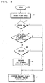
pel lines pel line 2 appears to the human eye to be a smooth gray scale picture. The sums of the gray levels ofpel lines pel lines pel lines - With reference to Figure 4, to remove the degradation in accordance with the present invention, starting at pel position (0,0),
control device 12 resets registers 1 and 4,X counter 27,Y counter 28 andY counter 35. In accordance with the present invention,control device 12 utilizes an odd column discrimination circuit 29, aline pattern generator 36 and a comparingcircuit 37 because, in this case, horizontal lines are inserted into the picture displayed onLCD device 25. It is assumed, for the purpose of the following description, that the 6 bit signals for all pels onlines CRT device 21 is 101010. - At
block 41,control device 12 stores the 6 bit signal 101010 for pel position (0,0) ofCRT device 21 inregister 1, and, inblock 42,control device 12 selects one of the dither tables, table 7. Atblock 43, any requirement for the addition of a horizontal line such asline 2 of the rightmost pel pattern in Figure 5 is determined. If not, operation proceeds to block 47. If so, as in the example case, operation proceeds to block 44. Atblock 44, comparingcircuit 31 compares the sum, +1 in this case, of the upper 2 values of dither table 7 with the sum, -1 in this case, of the lower 2 values of table 7. If the sums are equal, operation proceeds to block 47. If the sums are not equal, as in this case, then operation proceeds to block 45. Atblock 45, odd column discrimination circuit 29 determines whether the 6 bit signal is used for an odd column pel ofCRT display device 21. If so, operation proceeds to block 46. If not, as in this case, then operation proceeds to block 47. Atblock 47, adder 9 anddiscrimination device 10 generate, in the manner hereinbefore described, the gray levels, such as 0 and +1, of the upper two pels (on pel line 0) inarea 14A of the rightmost pel pattern in Figure 5. - Next, the gray levels of the upper two pels of
area 14B onpel line 0 of the rightmost pel pattern in Figure 5 are generated.X counter 27 is advanced to 1. Therefore,control device 12 stores the 6 bit signal 101010 of pel position (1, 0) inregister 1. Atblock 42, dither table 7 is selected, and operation proceeds to block 43 from which the response is YES. Atblock 44, the sum, +1, of the upper two values in table 7 are compared to the sum, -1, of the lower two values in table 7. Because the response fromblock 44 is NO, operation proceeds to block 45. Atblock 45, odd column discrimination circuit 29 determines whether the 6 bit signal is being used for an odd or an even column ofCRT device 21. Since pel position (1,0) is an odd column, the response fromblock 45 is YES. Specifically, odd column discrimination circuit 29 generates an output signal for activating anexchange circuit 32. Operation proceeds to block 46. AtBlock 46, the upper twovalues 0 and +1 of table 7 are exchanged with the lower twovalues 0 and -1, as shown in table 7A of Figure 5. Operation proceeds to block 47. Inblock 47,gray levels 0 and -1 of the upper two pels (on line 0) inarea 14B of the rightmost pattern of Figure 5 are generated. - To generate the gray level signals of the upper two pels of
area 14C of the rightmost pattern in Figure 5,X counter 27 is advanced to 2, andcontrol device 12 stores the 6 bit signal 101010 of pel position (2,0) ofCRT device 21 inregister 1. A similar operation to Operation A is then performed. However, in this case, the response ofblock 45 is NO. Therefore, the exchange of the values of table 7 inblock 46 is not performed. Thus, the gray level signals 0 and +1 for the upper two pels ofarea 14C are generated. - To generate the gray level signals of the upper two pels of
area 14D of the rightmost pattern in Figure 5,X counter 27 is advanced to 3, andcontrol device 12 stores the 6 bit signal 101010 of pel position (3,0) ofCRT device 21 inregister 1. A similar operation to Operation B is then performed. However, in this case, the response ofblock 45 is YES. Therefore, the exchange of values in table 7 inblock 46 is performed. Thus, the gray level signals 0 and -1 for the upper two pels of thearea 14D are generated. - In this manner, the 6 bit signals of
pel line 0 forCRT device 21 supplied fromcomputer 20 are sequentially stored inregister 1 and sequentially processed by the algorithm illustrated in Figure 4 to generate the gray level signals for pels onpel line 0 ofLCD device 25. The gray level signals are supplied todata driver 38 ofLCD device 25 for displaying the picture online 0. - The gray level signals for pels of
line 1 ofLCD device 25 are now generated. Since the 6 bit signals for pels online 0 ofCRT device 21 are used to generate the gray level signals for pels on bothlines LCD device 25, the above-mentioned 6 bit signals forpel line 0 ofCRT device 21 are again sequentially processed by the algorithm of Figure 4. However, the lower two values of tables 7 and 7A are used to generate the gray level signals of pels ofline 1 ofLCD device 25. In other words, the lower twovalues 0 and -1 of table 7 are used for evenareas values 0 and +1 of table 7A are used forodd areas -
Line 2 is now added afterline 1 of the rightmost pattern of Figure 5. When the gray scale signal of a pel online 1 ofLCD device 25 is supplied fromdata driver 38 to pels ofLCD device 25,gate lines gate driver 39.Y counter 35, aline pattern generator 36 and a comparingcircuit 37 insert the line.Y counter 35 is initially reset to 0, and then incremented bycontrol device 12.Control device 12 initially stores 1, 6, 11,... inline pattern generator 36 to indicate the lines after which a new line is added. Comparingcircuit 37 compares the value in Y counter 35 with the value inline pattern generator 36. If both values are equal, comparingcircuit 37 supplies a signal togate driver 39.Gate driver 39 sequentially activates the gate lines in synchronism withY counter 35 when the signal is not supplied from comparingcircuit 37. Whengate driver 39 is about to activateline 1, and the signal is supplied from comparingcircuit 37,gate driver 39 responds by simultaneously activating bothlines line 1 is thus simultaneously displayed online 2. The gray level signals forlines LCD device 25 are now generated in the same manner. - Referring to Figure 5, in the rightmost pattern, the 2x2 dither pel groups of the picture appear to the human eye as single pels. The sums of gray levels of pairs of
lines lines Lines - The dot patterns generated in accordance with the present invention via tables 6 and 8 are shown in the rightmost dot patterns in Figures 6 and 7. The sums, -4 and +4, of the gray levels of
lines lines - The same problem as that raised by inserting horizontal lines is also raised by inserting vertical columns. Although a Figure illustrating the insertion of vertical columns is excluded from the attached drawings, the problem will be easily understood by those skilled in the art by reference to Figures 12 to 14. Referring to Figure 8, the present invention prevents the introduction of a vertical pel column with different gray level to that of the remaining picture. The algorithm shown in Figure 8 is similar to that shown in Figure 4, except that
block 63 determines whether vertical pel columns should be inserted to expand, for example, 640 horizontal pels to 980 pels, block 64 determines whether the sum of the left two values in the dither matrix is equal to the sum of the right two values, block 65 determines whether the 6 bit signal is being used for an odd line ofCRT device 21, and block 66 exchanges the left two values and the right two values to generate a modified table, such as table 6A in Figure 9. Therefore, comparingcircuit 31 compares the sum of the left two values of the table with the right two values.Exchange circuit 32 exchanges the left two values and the right two values. -
Control device 12 initially resetsregisters X counter 27,Y counter 28,X counter 33.Control device 12 operates oddline discrimination circuit 30, acolumn pattern generator 34 and a comparingcircuit 40 because, in this case, pel columns are inserted. - The lower pattern in Figure 9 shows a
pel column 2 being added. In Figure 9, table 6 is used.Column 2 has the same pels ascolumn 1. The addition ofcolumn 2 aftercolumn 1 is performed byX counter 33,column pattern generator 34 and comparingcircuit 40. When the gray scale signal forcolumn 1 is supplied todata driver 38, the gray scale signal forcolumn 1 is copied into thenext column 2 so that the same gray scale pels as those ofcolumn 1 are displayed incolumn 2 ofLCD device 25. To perform the insertion,control device 12 initially storesvalue 1 corresponding tocolumn 1 incolumn pattern generator 34.X counter 33 is advanced from 0 to 1, 2, 3, .... . Comparingcircuit 40 compares the value inX counter 33 with the value incolumn pattern generator 34 and supplies a signal todata driver 38 when both values are equal, whereby the same gray level pels as those incolumn 1 are displayed incolumn 2. - Briefly describing the generation of the lower pattern in Figure 9 using the algorithm shown in Figure 8, the gray level signals of
line column 2 is added. For the processing oflines block 65 responds with the answer NO. Specifically, oddline discrimination circuit 30 does not supply the activation signal to exchangecircuit 32. When the 6 bit signals online 1 ofCRT device 21 are processed, oddline discrimination circuit 30 activatesexchange circuit 32 inblock 65, andexchange circuit 32 exchanges theright side value 0 and -1 and theleft side values block 66 to produce table 6A. The gray levels onlines LCD device 25 are thus displayed, as shown in the lower pattern of Figure 9. The operation is repeated to generate the gray scale signals oflines 4 to 7 of the lower pattern in Figure 9. - The resultant lower pattern in Figure 9 shows that the sum, -2, of the gray levels of
columns columns columns columns column - In the embodiments of the present invention hereinbefore described, the tables each included 2x2 matrices. However, it will be appreciated that any tables of PxQ modification values satisfying PxQ≥2N-M can be used. For example, a table including a 3x3 matrix is shown in Figure 10. To perform the exchange of values in the table in
block 46, the values in lines A, B and C in table 81 are exchanged to generate table 82, as shown in Figure 10. To perform the exchange inblock 66, the values in columns A, B and C in table 83 are exchanged to generate table 84. - As described hereinbefore, the present invention prevents the appearance of pel lines of different gray level through the insertion of horizontal pel lines or columns to the picture displayed on an LCD device. In accordance with the present invention, this is achieved by determining whether or not to shift compensation values in a dither matrix table depending on whether or not a corresponding pel line is to be inserted.
Claims (10)
- A display system for converting N bit signals each, representing 2N grey scale levels, to M bit signals representing 2M grey levels, where N is an integer larger than or equal to 2 and M is an integer satisfying N>M≥1, the system comprising:means (1) for separating each of the N bit signals into higher order M bits and N-M bits;2N-M tables (5,6,7,8) each storing a distinctive set of PxQ modification values satisfying PxQ≥2N-M:means (12) for selecting one of the tables as a function of the N-M bits;means (31) for detecting a difference between a first set of modification values and a second set of modification values of the selected table,means (32) for exchanging the first set of modification values and the second set of modification values to generate a modified table from the selected table;means (9) for adding the M bits of one N bit signal and each of the modification values of one of said modified or the selected table to generate a set of PxQ M bit signals; andmeans (10) for supplying the set of M bit signals to a display device of 2M grey levels.
- A display system according to Claim 1, wherein the system comprises means (35,36,37 & 33,34,40) for detecting the need to add a line or column, and wherein the detecting means and exchanging means are operable in response to said need.
- A display system according to Claim 1 or 2, wherein the system comprises means (27,29 & 28,30) for detecting whether a line or column is odd, and wherein the exchanging means are operable in response to said need.
- A display system according to Claim 1, 2 or 3, wherein the display device receives the first and second sets of PxQ M bit signals to display them on Q image lines and the same image as that of the Qth image line on one additional line.
- A display system as claimed in Claim 1, wherein said first set of modification values in said table are P modification values arranged in first horizontal line in said table, and said second set of modification values in said table are P modification values arranged in second horizontal line in said table.
- A display system as claimed in Claim 1, wherein said first set of modification values in said table are Q modification values arranged in first vertical column in said table, and said second set of modification values in said table are Q modification values arranged in second vertical line in said table.
- A method for converting N bit signals each, representing 2N grey levels, to M bit signals representing 2M grey levels, where N is an integer larger than or equal to 2 and M is an integer satisfying N>M≥1, said method comprising the steps of:separating (1) each of said N bit signals into higher M bits and lower N-M bits;creating 2N-M tables (5,6,7,8) each of which stores a distinct set of PxQ modification values satisfying PxQ≥2N-M;selecting (12) one of said tables using said N-M bits;conditionally detecting (31) unequality between first set of modification values and second set of modification values of said selected table;conditionally exchanging (32) said first set of modification values and said second set of modification values to generated a modified table from said selected table;adding (9) said M bits of one N bit signal and each of the modification values of one of said modified or said selected table to generate a set of PxQ M bit signals; andsupplying (10) said set of M bit signals to a display device of 2M grey levels.
- A method as claimed in Claim 7, wherein said display device receives said first and second sets of PxQ M bit signals to display them on Q image lines and the same image as that of Qth image line on one additional line.
- A method as claimed in Claim 7, wherein said first set of modification values in said table are P modification values arranged in first horizontal line in said table, and said second set of modification values in said table are P modification values arranged in second horizontal line in said table.
- A method as claimed in Claim 7, wherein said first set of modification values in said table are Q modification values arranged in first vertical column in said table, and said second set of modification values in said table are Q modification values arranged in second vertical column in said table.
Applications Claiming Priority (3)
| Application Number | Priority Date | Filing Date | Title |
|---|---|---|---|
| JP31881391 | 1991-12-03 | ||
| JP3318813A JPH0772824B2 (en) | 1991-12-03 | 1991-12-03 | Display system |
| JP318813/91 | 1991-12-03 |
Publications (3)
| Publication Number | Publication Date |
|---|---|
| EP0545577A2 EP0545577A2 (en) | 1993-06-09 |
| EP0545577A3 EP0545577A3 (en) | 1995-12-20 |
| EP0545577B1 true EP0545577B1 (en) | 2001-01-17 |
Family
ID=18103233
Family Applications (1)
| Application Number | Title | Priority Date | Filing Date |
|---|---|---|---|
| EP92310528A Expired - Lifetime EP0545577B1 (en) | 1991-12-03 | 1992-11-18 | Display system and method |
Country Status (10)
| Country | Link |
|---|---|
| US (1) | US5272471A (en) |
| EP (1) | EP0545577B1 (en) |
| JP (1) | JPH0772824B2 (en) |
| KR (1) | KR950014981B1 (en) |
| CN (1) | CN1040805C (en) |
| CA (1) | CA2079352C (en) |
| DE (1) | DE69231642T2 (en) |
| ES (1) | ES2153354T3 (en) |
| SG (1) | SG43735A1 (en) |
| TW (1) | TW216475B (en) |
Families Citing this family (20)
| Publication number | Priority date | Publication date | Assignee | Title |
|---|---|---|---|---|
| US5500924A (en) * | 1992-05-07 | 1996-03-19 | Apple Computer, Inc. | Method for vector plotting a bitmap with a reduced number of lines |
| US6118429A (en) | 1993-09-30 | 2000-09-12 | Hitachi, Ltd. | Liquid crystal display system capable of reducing and enlarging resolution of input display data |
| US5726718A (en) * | 1994-09-30 | 1998-03-10 | Texas Instruments Incorporated | Error diffusion filter for DMD display |
| JP3354741B2 (en) * | 1995-04-17 | 2002-12-09 | 富士通株式会社 | Halftone display method and halftone display device |
| US5977933A (en) * | 1996-01-11 | 1999-11-02 | S3, Incorporated | Dual image computer display controller |
| US5990858A (en) * | 1996-09-04 | 1999-11-23 | Bloomberg L.P. | Flat panel display terminal for receiving multi-frequency and multi-protocol video signals |
| US6295041B1 (en) * | 1997-03-05 | 2001-09-25 | Ati Technologies, Inc. | Increasing the number of colors output by an active liquid crystal display |
| DE69937029T9 (en) | 1998-10-12 | 2008-09-04 | Victor Company of Japan, Ltd., Yokohama | Signal processing method and device for gray scale video signal in a matrix display device |
| JP4637315B2 (en) | 1999-02-24 | 2011-02-23 | 株式会社半導体エネルギー研究所 | Display device |
| US7193594B1 (en) * | 1999-03-18 | 2007-03-20 | Semiconductor Energy Laboratory Co., Ltd. | Display device |
| US7145536B1 (en) | 1999-03-26 | 2006-12-05 | Semiconductor Energy Laboratory Co., Ltd. | Liquid crystal display device |
| US6952194B1 (en) | 1999-03-31 | 2005-10-04 | Semiconductor Energy Laboratory Co., Ltd. | Liquid crystal display device |
| US6753854B1 (en) * | 1999-04-28 | 2004-06-22 | Semiconductor Energy Laboratory Co., Ltd. | Display device |
| US6590581B1 (en) * | 1999-05-07 | 2003-07-08 | Semiconductor Energy Laboratory Co., Ltd. | Display device |
| JP3357666B2 (en) | 2000-07-07 | 2002-12-16 | 松下電器産業株式会社 | Display device and display method |
| US7330162B2 (en) * | 2002-02-28 | 2008-02-12 | Semiconductor Energy Laboratory Co., Ltd. | Method of driving a light emitting device and electronic equipment |
| TWI350501B (en) * | 2006-09-20 | 2011-10-11 | Novatek Microelectronics Corp | Method for dithering image data |
| CN201081774Y (en) * | 2006-12-21 | 2008-07-02 | 比亚迪股份有限公司 | Radial circuit for driving LCD |
| TWI395195B (en) * | 2008-07-30 | 2013-05-01 | Orise Technology Co Ltd | Method for applying the same dithering table for different flat panels and display driving method thereof |
| WO2011077926A1 (en) | 2009-12-24 | 2011-06-30 | Semiconductor Energy Laboratory Co., Ltd. | Display device and electronic device |
Family Cites Families (8)
| Publication number | Priority date | Publication date | Assignee | Title |
|---|---|---|---|---|
| JPS6069207A (en) * | 1983-09-14 | 1985-04-19 | Mazda Motor Corp | Eccentric shaft of multicylinder rotary piston engine |
| DE3751035T2 (en) * | 1986-12-04 | 1995-05-24 | Quantel Ltd | Video signal processing systems. |
| JPH0743580B2 (en) * | 1988-09-22 | 1995-05-15 | インターナショナル・ビジネス・マシーンズ・コーポレーション | How to convert gray scale |
| WO1990003019A1 (en) * | 1988-09-16 | 1990-03-22 | Chips And Technologies, Inc. | Compensation method and circuitry for flat panel display |
| US4956638A (en) * | 1988-09-16 | 1990-09-11 | International Business Machines Corporation | Display using ordered dither |
| JPH0650522B2 (en) * | 1988-09-22 | 1994-06-29 | インターナショナル・ビジネス・マシーンズ・コーポレーション | Display system |
| US5068649A (en) * | 1988-10-14 | 1991-11-26 | Compaq Computer Corporation | Method and apparatus for displaying different shades of gray on a liquid crystal display |
| EP0378780B1 (en) * | 1989-01-13 | 1994-05-04 | International Business Machines Corporation | Error propagated image halftoning with time-varying phase shift |
-
1991
- 1991-12-03 JP JP3318813A patent/JPH0772824B2/en not_active Expired - Lifetime
- 1991-12-11 TW TW080109718A patent/TW216475B/zh not_active IP Right Cessation
-
1992
- 1992-09-24 CA CA002079352A patent/CA2079352C/en not_active Expired - Fee Related
- 1992-10-07 US US07/957,562 patent/US5272471A/en not_active Expired - Lifetime
- 1992-11-18 EP EP92310528A patent/EP0545577B1/en not_active Expired - Lifetime
- 1992-11-18 DE DE69231642T patent/DE69231642T2/en not_active Expired - Fee Related
- 1992-11-18 ES ES92310528T patent/ES2153354T3/en not_active Expired - Lifetime
- 1992-11-18 SG SG1996000333A patent/SG43735A1/en unknown
- 1992-11-19 KR KR1019920021694A patent/KR950014981B1/en not_active IP Right Cessation
- 1992-11-19 CN CN92113166A patent/CN1040805C/en not_active Expired - Lifetime
Also Published As
| Publication number | Publication date |
|---|---|
| KR950014981B1 (en) | 1995-12-20 |
| CA2079352A1 (en) | 1993-06-04 |
| CN1040805C (en) | 1998-11-18 |
| JPH05241545A (en) | 1993-09-21 |
| DE69231642D1 (en) | 2001-02-22 |
| EP0545577A2 (en) | 1993-06-09 |
| JPH0772824B2 (en) | 1995-08-02 |
| EP0545577A3 (en) | 1995-12-20 |
| TW216475B (en) | 1993-11-21 |
| CA2079352C (en) | 1997-05-13 |
| US5272471A (en) | 1993-12-21 |
| DE69231642T2 (en) | 2001-06-21 |
| KR930013976A (en) | 1993-07-22 |
| ES2153354T3 (en) | 2001-03-01 |
| CN1073027A (en) | 1993-06-09 |
| SG43735A1 (en) | 1997-11-14 |
Similar Documents
| Publication | Publication Date | Title |
|---|---|---|
| EP0545577B1 (en) | Display system and method | |
| EP1168289B1 (en) | Display device for creating intermediate gradation levels in pseudo manner and imaging signal processing method | |
| KR100735783B1 (en) | Display device and display method | |
| US5552800A (en) | Color display control apparatus for controlling display gray scale of each scanning frame or each plurality of dots | |
| US5712651A (en) | Apparatus for performing a full-color emulation on the TFT display device | |
| US6310602B1 (en) | Liquid crystal display system capable of reducing and enlarging resolution of input display data | |
| KR100554580B1 (en) | Image processing apparatus, image processing method, image display apparatus, and mobile electronic device | |
| CA2017757C (en) | Method for driving display device | |
| EP0076082B1 (en) | Display processing apparatus | |
| US5623316A (en) | On-screen display apparatus and on-screen display method | |
| US20070176949A1 (en) | Dithering system | |
| US7268790B1 (en) | Display system with framestore and stochastic dithering | |
| US6295041B1 (en) | Increasing the number of colors output by an active liquid crystal display | |
| KR19980066488A (en) | Multi Gradient Processing Unit | |
| KR20020040642A (en) | Display apparatus displaying pseudo gray levels and method for displaying the same | |
| EP0346090B1 (en) | Graphic dot flare apparatus | |
| US4737778A (en) | Video display controller | |
| KR19980054752A (en) | Multi Gradient Processing Unit | |
| EP0400990B1 (en) | Apparatus for superimposing character patterns in accordance with dot-matrix on video signals | |
| US5920302A (en) | Display scrolling circuit | |
| KR100347491B1 (en) | Image Information Process Apparatus for Having a Display to Display Continuous Tones in a Pseudo Manner | |
| US6292162B1 (en) | Driving circuit capable of making a liquid crystal display panel display and expanded picture without special signal processor | |
| JPH11133931A (en) | Liquid crystal gradation display circuit | |
| JPH06161400A (en) | Gradational display system | |
| TW530290B (en) | Display device for creating intermediate gradation levels in pseudo manner and imaging signal processing method |
Legal Events
| Date | Code | Title | Description |
|---|---|---|---|
| PUAI | Public reference made under article 153(3) epc to a published international application that has entered the european phase |
Free format text: ORIGINAL CODE: 0009012 |
|
| AK | Designated contracting states |
Kind code of ref document: A2 Designated state(s): BE CH DE ES FR GB IT LI NL SE |
|
| 17P | Request for examination filed |
Effective date: 19931021 |
|
| PUAL | Search report despatched |
Free format text: ORIGINAL CODE: 0009013 |
|
| AK | Designated contracting states |
Kind code of ref document: A3 Designated state(s): BE CH DE ES FR GB IT LI NL SE |
|
| 17Q | First examination report despatched |
Effective date: 19980511 |
|
| RTI1 | Title (correction) |
Free format text: DISPLAY SYSTEM AND METHOD |
|
| GRAG | Despatch of communication of intention to grant |
Free format text: ORIGINAL CODE: EPIDOS AGRA |
|
| 17Q | First examination report despatched |
Effective date: 19980511 |
|
| GRAG | Despatch of communication of intention to grant |
Free format text: ORIGINAL CODE: EPIDOS AGRA |
|
| GRAH | Despatch of communication of intention to grant a patent |
Free format text: ORIGINAL CODE: EPIDOS IGRA |
|
| GRAH | Despatch of communication of intention to grant a patent |
Free format text: ORIGINAL CODE: EPIDOS IGRA |
|
| GRAA | (expected) grant |
Free format text: ORIGINAL CODE: 0009210 |
|
| AK | Designated contracting states |
Kind code of ref document: B1 Designated state(s): BE CH DE ES FR GB IT LI NL SE |
|
| PG25 | Lapsed in a contracting state [announced via postgrant information from national office to epo] |
Ref country code: NL Free format text: LAPSE BECAUSE OF FAILURE TO SUBMIT A TRANSLATION OF THE DESCRIPTION OR TO PAY THE FEE WITHIN THE PRESCRIBED TIME-LIMIT Effective date: 20010117 Ref country code: FR Free format text: LAPSE BECAUSE OF FAILURE TO SUBMIT A TRANSLATION OF THE DESCRIPTION OR TO PAY THE FEE WITHIN THE PRESCRIBED TIME-LIMIT Effective date: 20010117 Ref country code: BE Free format text: LAPSE BECAUSE OF FAILURE TO SUBMIT A TRANSLATION OF THE DESCRIPTION OR TO PAY THE FEE WITHIN THE PRESCRIBED TIME-LIMIT Effective date: 20010117 |
|
| ITF | It: translation for a ep patent filed |
Owner name: BRAVI ALFREDO DR. |
|
| REG | Reference to a national code |
Ref country code: CH Ref legal event code: NV Representative=s name: JULIAN DAVID WILLIAMS C/O INTERNATIONAL BUSINESS M Ref country code: CH Ref legal event code: EP |
|
| REF | Corresponds to: |
Ref document number: 69231642 Country of ref document: DE Date of ref document: 20010222 |
|
| REG | Reference to a national code |
Ref country code: ES Ref legal event code: FG2A Ref document number: 2153354 Country of ref document: ES Kind code of ref document: T3 |
|
| EN | Fr: translation not filed | ||
| NLV1 | Nl: lapsed or annulled due to failure to fulfill the requirements of art. 29p and 29m of the patents act | ||
| PGFP | Annual fee paid to national office [announced via postgrant information from national office to epo] |
Ref country code: SE Payment date: 20011019 Year of fee payment: 10 |
|
| PGFP | Annual fee paid to national office [announced via postgrant information from national office to epo] |
Ref country code: ES Payment date: 20011122 Year of fee payment: 10 |
|
| PLBE | No opposition filed within time limit |
Free format text: ORIGINAL CODE: 0009261 |
|
| STAA | Information on the status of an ep patent application or granted ep patent |
Free format text: STATUS: NO OPPOSITION FILED WITHIN TIME LIMIT |
|
| PG25 | Lapsed in a contracting state [announced via postgrant information from national office to epo] |
Ref country code: LI Free format text: LAPSE BECAUSE OF NON-PAYMENT OF DUE FEES Effective date: 20011130 Ref country code: CH Free format text: LAPSE BECAUSE OF NON-PAYMENT OF DUE FEES Effective date: 20011130 |
|
| REG | Reference to a national code |
Ref country code: GB Ref legal event code: IF02 |
|
| 26N | No opposition filed | ||
| REG | Reference to a national code |
Ref country code: CH Ref legal event code: PL |
|
| PG25 | Lapsed in a contracting state [announced via postgrant information from national office to epo] |
Ref country code: SE Free format text: LAPSE BECAUSE OF NON-PAYMENT OF DUE FEES Effective date: 20021119 Ref country code: ES Free format text: LAPSE BECAUSE OF NON-PAYMENT OF DUE FEES Effective date: 20021119 |
|
| EUG | Se: european patent has lapsed | ||
| REG | Reference to a national code |
Ref country code: ES Ref legal event code: FD2A Effective date: 20031213 |
|
| REG | Reference to a national code |
Ref country code: GB Ref legal event code: 732E |
|
| PGFP | Annual fee paid to national office [announced via postgrant information from national office to epo] |
Ref country code: GB Payment date: 20061122 Year of fee payment: 15 |
|
| PGFP | Annual fee paid to national office [announced via postgrant information from national office to epo] |
Ref country code: IT Payment date: 20061130 Year of fee payment: 15 |
|
| PGFP | Annual fee paid to national office [announced via postgrant information from national office to epo] |
Ref country code: DE Payment date: 20070102 Year of fee payment: 15 |
|
| GBPC | Gb: european patent ceased through non-payment of renewal fee |
Effective date: 20071118 |
|
| PG25 | Lapsed in a contracting state [announced via postgrant information from national office to epo] |
Ref country code: DE Free format text: LAPSE BECAUSE OF NON-PAYMENT OF DUE FEES Effective date: 20080603 |
|
| PG25 | Lapsed in a contracting state [announced via postgrant information from national office to epo] |
Ref country code: GB Free format text: LAPSE BECAUSE OF NON-PAYMENT OF DUE FEES Effective date: 20071118 |
|
| PG25 | Lapsed in a contracting state [announced via postgrant information from national office to epo] |
Ref country code: IT Free format text: LAPSE BECAUSE OF NON-PAYMENT OF DUE FEES Effective date: 20071118 |