EP0543391A2 - Photoelectric conversion device and method of driving the same - Google Patents
Photoelectric conversion device and method of driving the same Download PDFInfo
- Publication number
- EP0543391A2 EP0543391A2 EP92119795A EP92119795A EP0543391A2 EP 0543391 A2 EP0543391 A2 EP 0543391A2 EP 92119795 A EP92119795 A EP 92119795A EP 92119795 A EP92119795 A EP 92119795A EP 0543391 A2 EP0543391 A2 EP 0543391A2
- Authority
- EP
- European Patent Office
- Prior art keywords
- photoelectric conversion
- layer
- forbidden band
- conversion device
- band
- Prior art date
- Legal status (The legal status is an assumption and is not a legal conclusion. Google has not performed a legal analysis and makes no representation as to the accuracy of the status listed.)
- Granted
Links
- 238000006243 chemical reaction Methods 0.000 title claims abstract description 131
- 238000000034 method Methods 0.000 title claims description 41
- 125000005842 heteroatom Chemical group 0.000 claims abstract description 50
- 239000004065 semiconductor Substances 0.000 claims abstract description 26
- 230000005764 inhibitory process Effects 0.000 claims abstract description 11
- 238000002347 injection Methods 0.000 claims abstract description 11
- 239000007924 injection Substances 0.000 claims abstract description 11
- 239000012535 impurity Substances 0.000 claims description 54
- 210000003127 knee Anatomy 0.000 claims description 29
- 238000003860 storage Methods 0.000 claims description 22
- 229920006395 saturated elastomer Polymers 0.000 claims description 11
- 239000010410 layer Substances 0.000 description 195
- 239000000758 substrate Substances 0.000 description 34
- BLRPTPMANUNPDV-UHFFFAOYSA-N Silane Chemical compound [SiH4] BLRPTPMANUNPDV-UHFFFAOYSA-N 0.000 description 21
- 230000005684 electric field Effects 0.000 description 18
- 239000000463 material Substances 0.000 description 18
- 238000005137 deposition process Methods 0.000 description 15
- 230000035945 sensitivity Effects 0.000 description 13
- 230000000903 blocking effect Effects 0.000 description 10
- 238000004519 manufacturing process Methods 0.000 description 9
- 229910000577 Silicon-germanium Inorganic materials 0.000 description 7
- 238000005268 plasma chemical vapour deposition Methods 0.000 description 7
- VYPSYNLAJGMNEJ-UHFFFAOYSA-N silicon dioxide Inorganic materials O=[Si]=O VYPSYNLAJGMNEJ-UHFFFAOYSA-N 0.000 description 7
- 238000005229 chemical vapour deposition Methods 0.000 description 6
- 238000005516 engineering process Methods 0.000 description 6
- QUZPNFFHZPRKJD-UHFFFAOYSA-N germane Chemical compound [GeH4] QUZPNFFHZPRKJD-UHFFFAOYSA-N 0.000 description 6
- 229910052986 germanium hydride Inorganic materials 0.000 description 6
- 238000004544 sputter deposition Methods 0.000 description 6
- 239000013078 crystal Substances 0.000 description 4
- 230000006866 deterioration Effects 0.000 description 4
- 229910003465 moissanite Inorganic materials 0.000 description 4
- 229910010271 silicon carbide Inorganic materials 0.000 description 4
- 235000012239 silicon dioxide Nutrition 0.000 description 4
- 229910004469 SiHx Inorganic materials 0.000 description 3
- 229910021417 amorphous silicon Inorganic materials 0.000 description 3
- FFBHFFJDDLITSX-UHFFFAOYSA-N benzyl N-[2-hydroxy-4-(3-oxomorpholin-4-yl)phenyl]carbamate Chemical compound OC1=C(NC(=O)OCC2=CC=CC=C2)C=CC(=C1)N1CCOCC1=O FFBHFFJDDLITSX-UHFFFAOYSA-N 0.000 description 3
- 229910052681 coesite Inorganic materials 0.000 description 3
- 230000000052 comparative effect Effects 0.000 description 3
- 229910052906 cristobalite Inorganic materials 0.000 description 3
- 238000010586 diagram Methods 0.000 description 3
- 230000000694 effects Effects 0.000 description 3
- 239000002184 metal Substances 0.000 description 3
- 229910052751 metal Inorganic materials 0.000 description 3
- 239000013081 microcrystal Substances 0.000 description 3
- 230000003287 optical effect Effects 0.000 description 3
- 239000002245 particle Substances 0.000 description 3
- 229920002120 photoresistant polymer Polymers 0.000 description 3
- 239000000377 silicon dioxide Substances 0.000 description 3
- 229910052682 stishovite Inorganic materials 0.000 description 3
- 229910052905 tridymite Inorganic materials 0.000 description 3
- XDLMVUHYZWKMMD-UHFFFAOYSA-N 3-trimethoxysilylpropyl 2-methylprop-2-enoate Chemical compound CO[Si](OC)(OC)CCCOC(=O)C(C)=C XDLMVUHYZWKMMD-UHFFFAOYSA-N 0.000 description 2
- 238000010521 absorption reaction Methods 0.000 description 2
- 230000001133 acceleration Effects 0.000 description 2
- 238000004891 communication Methods 0.000 description 2
- 230000000779 depleting effect Effects 0.000 description 2
- 238000002161 passivation Methods 0.000 description 2
- XOLBLPGZBRYERU-UHFFFAOYSA-N tin dioxide Chemical compound O=[Sn]=O XOLBLPGZBRYERU-UHFFFAOYSA-N 0.000 description 2
- 229910003811 SiGeC Inorganic materials 0.000 description 1
- 229910004541 SiN Inorganic materials 0.000 description 1
- 229910020328 SiSn Inorganic materials 0.000 description 1
- 238000002441 X-ray diffraction Methods 0.000 description 1
- 229910017875 a-SiN Inorganic materials 0.000 description 1
- 239000002253 acid Substances 0.000 description 1
- 239000003513 alkali Substances 0.000 description 1
- 229910052782 aluminium Inorganic materials 0.000 description 1
- 229910052787 antimony Inorganic materials 0.000 description 1
- 229910052785 arsenic Inorganic materials 0.000 description 1
- 238000000098 azimuthal photoelectron diffraction Methods 0.000 description 1
- 229910052790 beryllium Inorganic materials 0.000 description 1
- 229910052797 bismuth Inorganic materials 0.000 description 1
- 229910052796 boron Inorganic materials 0.000 description 1
- 229910052793 cadmium Inorganic materials 0.000 description 1
- 229910052791 calcium Inorganic materials 0.000 description 1
- 229910052799 carbon Inorganic materials 0.000 description 1
- 239000000919 ceramic Substances 0.000 description 1
- 230000008602 contraction Effects 0.000 description 1
- 238000002425 crystallisation Methods 0.000 description 1
- 230000008025 crystallization Effects 0.000 description 1
- 238000000151 deposition Methods 0.000 description 1
- 230000008021 deposition Effects 0.000 description 1
- 230000005611 electricity Effects 0.000 description 1
- 230000001747 exhibiting effect Effects 0.000 description 1
- 229910052733 gallium Inorganic materials 0.000 description 1
- 229910052732 germanium Inorganic materials 0.000 description 1
- 239000011521 glass Substances 0.000 description 1
- 238000003384 imaging method Methods 0.000 description 1
- 229910052738 indium Inorganic materials 0.000 description 1
- 230000010365 information processing Effects 0.000 description 1
- 150000002500 ions Chemical class 0.000 description 1
- VRIVJOXICYMTAG-IYEMJOQQSA-L iron(ii) gluconate Chemical compound [Fe+2].OC[C@@H](O)[C@@H](O)[C@H](O)[C@@H](O)C([O-])=O.OC[C@@H](O)[C@@H](O)[C@H](O)[C@@H](O)C([O-])=O VRIVJOXICYMTAG-IYEMJOQQSA-L 0.000 description 1
- 229910052749 magnesium Inorganic materials 0.000 description 1
- 229910052753 mercury Inorganic materials 0.000 description 1
- 229910044991 metal oxide Inorganic materials 0.000 description 1
- 150000004706 metal oxides Chemical class 0.000 description 1
- 239000000203 mixture Substances 0.000 description 1
- 229910052698 phosphorus Inorganic materials 0.000 description 1
- 229910052699 polonium Inorganic materials 0.000 description 1
- -1 polycrystal Substances 0.000 description 1
- 239000010453 quartz Substances 0.000 description 1
- 239000011347 resin Substances 0.000 description 1
- 229920005989 resin Polymers 0.000 description 1
- 229910052711 selenium Inorganic materials 0.000 description 1
- 229910052710 silicon Inorganic materials 0.000 description 1
- LIVNPJMFVYWSIS-UHFFFAOYSA-N silicon monoxide Inorganic materials [Si-]#[O+] LIVNPJMFVYWSIS-UHFFFAOYSA-N 0.000 description 1
- 239000002356 single layer Substances 0.000 description 1
- 239000007787 solid Substances 0.000 description 1
- 239000002904 solvent Substances 0.000 description 1
- 229910052712 strontium Inorganic materials 0.000 description 1
- 239000000126 substance Substances 0.000 description 1
- 229910052717 sulfur Inorganic materials 0.000 description 1
- 229910052715 tantalum Inorganic materials 0.000 description 1
- 229910052714 tellurium Inorganic materials 0.000 description 1
- 229910052725 zinc Inorganic materials 0.000 description 1
Images


Classifications
-
- H—ELECTRICITY
- H10—SEMICONDUCTOR DEVICES; ELECTRIC SOLID-STATE DEVICES NOT OTHERWISE PROVIDED FOR
- H10F—INORGANIC SEMICONDUCTOR DEVICES SENSITIVE TO INFRARED RADIATION, LIGHT, ELECTROMAGNETIC RADIATION OF SHORTER WAVELENGTH OR CORPUSCULAR RADIATION
- H10F77/00—Constructional details of devices covered by this subclass
- H10F77/10—Semiconductor bodies
- H10F77/14—Shape of semiconductor bodies; Shapes, relative sizes or dispositions of semiconductor regions within semiconductor bodies
-
- H—ELECTRICITY
- H10—SEMICONDUCTOR DEVICES; ELECTRIC SOLID-STATE DEVICES NOT OTHERWISE PROVIDED FOR
- H10F—INORGANIC SEMICONDUCTOR DEVICES SENSITIVE TO INFRARED RADIATION, LIGHT, ELECTROMAGNETIC RADIATION OF SHORTER WAVELENGTH OR CORPUSCULAR RADIATION
- H10F30/00—Individual radiation-sensitive semiconductor devices in which radiation controls the flow of current through the devices, e.g. photodetectors
- H10F30/20—Individual radiation-sensitive semiconductor devices in which radiation controls the flow of current through the devices, e.g. photodetectors the devices having potential barriers, e.g. phototransistors
- H10F30/21—Individual radiation-sensitive semiconductor devices in which radiation controls the flow of current through the devices, e.g. photodetectors the devices having potential barriers, e.g. phototransistors the devices being sensitive to infrared, visible or ultraviolet radiation
- H10F30/22—Individual radiation-sensitive semiconductor devices in which radiation controls the flow of current through the devices, e.g. photodetectors the devices having potential barriers, e.g. phototransistors the devices being sensitive to infrared, visible or ultraviolet radiation the devices having only one potential barrier, e.g. photodiodes
- H10F30/225—Individual radiation-sensitive semiconductor devices in which radiation controls the flow of current through the devices, e.g. photodetectors the devices having potential barriers, e.g. phototransistors the devices being sensitive to infrared, visible or ultraviolet radiation the devices having only one potential barrier, e.g. photodiodes the potential barrier working in avalanche mode, e.g. avalanche photodiodes
- H10F30/2255—Individual radiation-sensitive semiconductor devices in which radiation controls the flow of current through the devices, e.g. photodetectors the devices having potential barriers, e.g. phototransistors the devices being sensitive to infrared, visible or ultraviolet radiation the devices having only one potential barrier, e.g. photodiodes the potential barrier working in avalanche mode, e.g. avalanche photodiodes in which the active layers form heterostructures, e.g. SAM structures
-
- H—ELECTRICITY
- H10—SEMICONDUCTOR DEVICES; ELECTRIC SOLID-STATE DEVICES NOT OTHERWISE PROVIDED FOR
- H10F—INORGANIC SEMICONDUCTOR DEVICES SENSITIVE TO INFRARED RADIATION, LIGHT, ELECTROMAGNETIC RADIATION OF SHORTER WAVELENGTH OR CORPUSCULAR RADIATION
- H10F39/00—Integrated devices, or assemblies of multiple devices, comprising at least one element covered by group H10F30/00, e.g. radiation detectors comprising photodiode arrays
- H10F39/10—Integrated devices
- H10F39/12—Image sensors
- H10F39/18—Complementary metal-oxide-semiconductor [CMOS] image sensors; Photodiode array image sensors
- H10F39/184—Infrared image sensors
- H10F39/1843—Infrared image sensors of the hybrid type
Definitions
- the present invention relates to a photoelectric conversion device and a method of driving the same, and, more particularly to a photoelectric conversion device and a method of driving the same which is capable of, at the time of performing an operation of storing charges into an avalanche photodiode (APD), lowering the driving voltage of the photoelectric conversion device while having Knee characteristics.
- APD avalanche photodiode
- an elongated line sensor comprising photosensors, which are one-dimensionally arranged, and an area sensor comprising the same which are two-dimensionally arranged, have been widely used with wide use of image information processing apparatuses such as facsimile machines, digital copying machines, image readers, and video cameras.
- a solid-state image sensing device such as a CCD, a bipolar transistor, or a MOS-type solid-state image sensing device have been used.
- a solid-state image sensing device such as a CCD, a bipolar transistor, or a MOS-type solid-state image sensing device have been used.
- incident light has been used effectively by utilizing a spherical lens or by employing a structure in which a photoelectric conversion device made of a material such as amorphous silicon is stacked on a CCD or the like.
- a peculiar problem of the noise of the transfer system has remained unsolved.
- avalanche photodiode (APD) which relatively eliminate the noise of the transfer system by amplifying the optical signal in a photoelectric conversion device (refer to "Shin-Gaku Giho" Vol. 86, No. 208, '86),
- the APDs are diodes which are widely used in the optical communication field and which are capable of amplifying the output to a degree of several tens to hundreds times. If the APD can be applied to an image pickup device, it can be expected that the S/N ratio can be satisfactorily improved.
- the ordinary APD for use in the optical communication field requires a considerably high voltage of several tens to hundreds volts because avalanche multiplication is induced by acceleration of the electric field of the carrier which is realized by an application of high voltage between two terminals of the device, and therefore the APD is not a normal power source for driving a solid sate imaging device.
- the fact that the avalanche multiplication considerably depends upon the intensity of the electric field has no region from which a linear output can be obtained with respect to the intensity of input light when the avalanche multiplication is considered to be utilized in a charge storage mode which is an ordinary method of driving the solid-state image sensing device.
- an improvement means has been developed (ITEJ Technical Report Vol. 11, No. 28, pp67 to 72) which has an additional capacity provided for the charge storage portion so as to restrict the change of the electric field taken place due to the charge storage, so that the linearity of the input and that of the output are maintained.
- deterioration of the linearity of the input and the output cannot be perfectly prevented when the voltage of the output signal component has been changed, while remaining the problem unsolved in that a high voltage power source must be used.
- each of the inclined layers it is necessary for each of the inclined layers to be applied with a voltage of 1 to 2 V by the number of times which correspond to the number of the inclined layers because the voltage to be applied to the multiplication layer can be reduced to a level which is able to deplete each of the inclined band gap layers. For example, it is sufficient to apply a voltage of 10V in the case where, for example, there are five inclined layers to each of which a voltage of 2V is added.
- the aforesaid photoelectric conversion device cannot be prevent the deterioration of the dynamic range depending upon the driving conditions such as the applied bias because it is designed for the purpose of mainly obtaining stable linearity of the input and the output, that is, even if the effective bias applied to the device has been changed during the charge storage operation, the carrier multiplication is not changed.
- Fig. 1 illustrates an energy band which shows the structure of a conventional photoelectric conversion device disclosed in International Laid-Open No. WO91/02381.
- Fig. 1A illustrates an energy band realized when no bias is applied to an APD having, as the device structure, a carrier multiplication portion formed by three stages.
- symbol Eg1 represents a required forbidden band
- Eg2 represents a minimum forbidden band
- Eg3 represents a maximum forbidden band.
- Symbol V0 represents energy which is the difference (x2 - x3) between electron affinity x2 of a material of Eg2 and electron affinity x3 of a material of Eg3.
- Fig. 3B illustrates an energy band realized when a bias required to cause a carrier multiplication to take place is applied.
- symbol E ion represents carrier ionizing energy
- V0 represents energy which is the difference (x2 - x3) between electron affinity x2 of a material of Eg2 and electron affinity x3 of a material of Eg3.
- Symbol V DA represents energy obtained by adding an energy step, which corresponds to the accelerated electric field, to V0, the aforesaid V DA having a relationship V DA ⁇ E ION ⁇ V0.
- Fig. 2 is a graph which illustrates characteristics between electric currents and voltages of an photoelectric conversion device of a type arranged as shown in Fig. 1.
- the structure shown in Fig. 1 is arranged in such a manner that the minimum forbidden band is subjected to a high density n-type doping because the band offset energy of the conductive zone of the hetero junction portion between the inclined band gap layers realized due to the carrier multiplication is lower than the energy for ionizing the minimum band gap portion, so that an electric field concentration is taken place when the bias is applied to the device in order to cause the electron ionization to take place.
- the APD structured into a high-density n-type semiconductor by subjecting its minimum forbidden band to a high density n-type doping among the aforesaid conventional APD designed to utilize the electron multiplication to be additionally applied with voltages of about 20, 40 and 60V after an electric current, which corresponds to a quantum efficiency of 1 at 14 to 15V, starts passing until multiplications of 2, 4 and 8 times take place.
- the aforesaid voltage levels are high levels comparing to the voltage levels which have raised a problem to be solved by the conventional APD of the electric field acceleration type. Therefore, it can be said that the aforesaid requirement is no practical use.
- the conventional photoelectric conversion device arranged in such a manner that the high density n-type semiconductor is disposed in the hetero junction portion between the maximum forbidden band layer and the minimum forbidden band layer for the purpose of preventing reduction of the dynamic range of the APD designed to utilize the electron multiplication and having a structure realized by repeating the inclined band gap layers encounters an unsolved problem that high voltage must be applied when it is driven.
- Fig. 3A illustrates an energy band realized when no bias is applied to another APD having, as the device structure, a carrier multiplication portion composed of three stages
- Fig. 3B illustrates an energy band realized when a bias required for a carrier multiplication to take place.
- symbol V0 represents energy which is the difference (x2 - x3) between electron affinity x2 of a material of Eg2 and electron affinity x3 of a material of Eg3
- V D represents energy of the step of the conductive band of the hetero junction portion realized when the bias is applied
- Fig. 4 is a graph which illustrates the characteristics of the APD shown in Fig. 3 between electric currents and voltages.
- the band offset energy of the hetero junction portion between the inclined band gap layers for the carrier multiplication exceeds the energy for ionizing the minimum band gap portion at the moment of the zero bias. Therefore, all of the inclined band gap layers are substantially simultaneously depleted with the progress of the bias application to the device. If the voltage exceeds depleting voltage V dep as shown in Fig. 4, a large electric current, which corresponds to about a quantum efficiency of 8, starts passing rapidly.
- Fig. 5 illustrates the relationship (solid line) between the input and the output from the conventional photoelectric conversion device realized when a charge is stored thereto and the relationship (dashed line) between the same of a device of a type having a quantum efficiency of 1.
- the device, on which the APD is mounted encounters the reduction of a saturated light quantity and the contraction of the dynamic range although the sensitivity can be improved.
- a photoelectric conversion device designed for the purpose of mainly obtaining high sensitive output and a method of driving the same encounter a problem in that the dynamic range is undesirably contracted.
- An object of the present invention is provide a photoelectric conversion device which is capable of overcoming the aforesaid conventional problem, which is arranged to utilize multiplication of electrons, on which an APD having a structure formed by repeating inclined band gaps is mounted, which is capable of performing a storage operation while having Knee characteristics, and which can be driven by minimized voltage, and a method of driving the same.
- Another object of the present invention is to provide a photoelectric conversion device capable of maintaining a wide dynamic range while preventing deterioration of the S/N ratio and a method of driving the same.
- a photoelectric conversion device comprising: a photoelectric conversion portion having a light absorbing layer disposed between charge injection inhibition layers and having a predetermined forbidden band width Eg1, and a carrier multiplication portion including a single or a plurality of inclined band gap layers, the inclined band gap layer including a minimum forbidden band width Eg2 and a maximum forbidden band width Eg3 which are disposed to be in contact with each other to form a hetero junction and having, at the two ends thereof, forbidden band widths Eg4 which holds a relationship Eg2 ⁇ Eg4 ⁇ Eg3 in such a manner that the forbidden band width is continuously changed from the two forbidden band widths Eg2 and Eg3 to the forbidden band width Eg4, and the energy step in a conductive band of the hetero junction portion is larger than the energy step in a valence electron band, wherein at least the minimum forbidden band width Eg2 of portions which form the hetero junction is made of a high density
- the voltage which must be applied to the device can be lowered by making the impurity to be the accepter and by using p-type semiconductor because the electric field acting on the light absorbing layer can be reduced.
- a photoelectric conversion device comprising: a photoelectric conversion portion having a light absorbing layer disposed between charge injection inhibition layers and having a predetermined forbidden band width Eg1, and a carrier multiplication portion including a single or a plurality of inclined band gap layers, the inclined band gap layer including a minimum forbidden band width Eg2 and a maximum forbidden band width Eg3 which are disposed to be in contact with each other to form a hetero junction and having, at the two ends thereof, forbidden band widths Eg4 which holds a relationship Eg2 ⁇ Eg4 ⁇ Eg3 in such a manner that the forbidden band width is continuously changed from the two forbidden band widths Eg2 and Eg3 to the forbidden band width Eg4, and the energy step in a conductive band of the hetero junction portion is larger than the energy step in a valence electron band, wherein at least the minimum forbidden band width Eg2 of portions which form the hetero junction is made of a high density
- the voltage which must be applied to the device can be lowered by making the impurity to be donor and by using n-type semiconductor because the electric field acting on the light absorbing layer can be reduced.
- Fig. 6A is a cross sectional view which illustrates the structure of an embodiment of a photoelectric conversion device according to the present invention.
- reference numeral 602 represents a MOS source or MOS drain serving as a switch device formed on a substrate 600, and 604 represents its drain.
- Reference numeral 611 represents a hole blocking layer (a charge injection inhibition layer)
- 612 represents a carrier multiplication portion
- 613 represents alight absorption layer
- 614 represents an electron blocking layer (a charge injection inhibition layer)
- 616 represents an upper electrode
- 615 represents a passivation layer.
- the carrier multiplication portion 612 is composed of three layers 612a, 612b and 612c and constituting, together with the light absorbing layer 613, a photoelectric conversion portion.
- the layer 612b which constitutes the three-layered carrier multiplication portion 612 is formed into a high density p-type layer.
- the thickness of the employed material may be determined to be a value which is about an average free stroke of the multiplication carrier. If the thickness is determined, the thickness of a single layer of the inclined band gap layer is determined. The thickness must be about three times the thickness of an impurity additional layer of the hetero junction portion, preferably about 10 to 20 times.
- the thickness and the quantity of the added impurities of the impurity additional layer of the hetero junction portion for concentrating the electric field in order to compensate the wanting offset energy may be determined as follows.
- the quantity of impurities to be added is determined to a value with which the voltage to be applied when the impurity layer has been completely depleted is higher than the quantity of the wanting offset energy. That is, it is determined as follows:
- Fig. 7A is a cross sectional structural view which illustrates another embodiment of the photoelectric conversion device according to the present invention, wherein the structure which is formed in the case where the carrier to be multiplied is a positive hole.
- reference numeral 602 represents a MOS source or MOS drain serving as a switch device formed on a substrate 600, and 604 represents its drain.
- Reference numeral 611 represents an electron blocking layer (a charge injection inhibition layer)
- 612 represents a carrier multiplication portion
- 613 represents alight absorption layer
- 614 represents a positive hole blocking layer (a charge injection inhibition layer)
- 616 represents an upper electrode
- 615 represents a passivation layer.
- the carrier multiplication portion 612 is composed of three layers 612a, 612b and 612c and constituting, together with the light absorbing layer 613, a photoelectric conversion portion. Furthermore, the layer 612b which constitutes the three-layered carrier multiplication portion 612 is formed into a high density p-type layer.
- the thickness and the quantity of the added impurities of the impurity additional layer of the hetero junction portion for concentrating the electric field in order to compensate the wanting offset energy may be determined as follows.
- the quantity of impurities to be added is determined to a value with which the voltage to be applied when the impurity layer has been completely depleted is higher than the quantity of the wanting offset energy. That is, it is determined as follows:
- Fig. 8 illustrates another embodiment of the photoelectric conversion device according to the present invention, wherein Fig. 8A is a cross sectional structural view, Fig. 8B illustrates an energy band realized when no bias is applied, and Fig. 8C illustrates an energy band realized when a bias required to cause the carrier multiplication to take place.
- the energy band of the present invention shown in Fig. 8 is different from it in a fact that there is no increase of the energy step due to the application of the bias because the hetero junction portion is not subjected to the impurity doping.
- the aforesaid fact is a characteristic of the driving method according to the present invention.
- Fig. 9 is a graph which illustrates the characteristics of the APD between electric currents and voltages, the APD having, as the device structure, a carrier multiplication portion composed of three stages.
- an electric current corresponding to a quantum efficiency 2 starts passing at a position in the neighborhood of ionization commencement voltage 1V ion1 , and then an electric current corresponding to quantum efficiencies 4 and 8 starts gradually passing at positions in the neighborhood of V ion2 and V ion3 .
- Fig. 10 illustrates the relationship between inputs and outputs realized when the storage operation is performed by applying a bias higher than V ion3 to the device according to this embodiment.
- the output is changed in this way that its inclination with respect to the input is changed if it exceeds a certain light quantity to become moderate by a degree corresponding to the step of the current-voltage characteristics until it is saturated.
- Output saturation characteristics of the aforesaid type can be approximately assumed to be a so-called Knee characteristics with which the dynamic range can be widened.
- the dynamic range can be widened by a degree (about 8 times according to this embodiment) which equivalents to the multiplication ratio in comparison to the case where the output has no Knee characteristics by superposing the boundary of the subject light quantity region on a point at which the saturation characteristics are commenced.
- Fig. 11 illustrates an example of the structure of a circuit for use in the photoelectric conversion device according to the present invention.
- the charge which has been generated in a photoelectric conversion device PD before it is multiplied, is divided into a portion to be stored in a capacity C PD of the PD and a portion to be stored in a junction capacity C D of the source portion of the switch MOS transistor Tr H .
- the quantity of the impurities to be added must be determined to a value with which the voltage which is applied when the impurity layer has been completely depleted made higher than the wanting quantity of the offset energy. That is, it is determined as follows depending upon the fact that the impurity layers are disposed at the two ends of the inclined band gap layer and the fact that the same is disposed at an end of the inclined band gap layer.
- the quantity in the case of the positive current is determined by the factors expressed as follows:
- the bias voltage V V to be applied to the photoelectric conversion device thus manufactured is obtained by using the following parameter in accordance with Equation (21):
- any one of an insulating substrate, a semiconductor substrate or a metal substrate may be employed if it is able to resist the temperature at the time of the deposition of the films on the substrate, an acid, alkali and a solvent for use to perform the required processes.
- insulating substrates of a type arranged in such a manner that switch devices and scanning devices are formed on glass, quartz or ceramics are widely used.
- a heat resisting resin film is employed.
- Semiconductor substrates of a type having a signal processing circuit such as a switch device, an amplifier, and a scanning device are employed.
- the signal processing circuit is typified by a CCD device, a MOS device, a BBD device and an image sensor disclosed in U.S. Patent No. 4,791,469 and arranged in such a manner that an emitter of a bipolar phototransistor is connected to an output circuit including a capacity load.
- either side employs a light transmissive electrode for receiving incidental light, the light transmissive electrode being exemplified by a metal film having a thickness of tens to hundreds of ⁇ and a conductive metal oxide film made of SnO2, ITO, ZnO2, IrO x or the like.
- the residual side is usually made of a metal film which may be selected from a group which meets required conditions such as resistance and chemical properties.
- a semiconductor As the photoconductive film and a carrier multiplication portion, a semiconductor, the valence electron thereof can be controlled, can be employed in the present invention, the semiconductor being exemplified by a tetrahedral (group IV) semiconductor or a composition semiconductor of groups III to V.
- Semiconductors of group IV are exemplified by Ge, Si, C and their complexes SiGe, SiC, SiGeC, and SiN, SiO and SiSn.
- the i-layer portion (non-dope or a small quantity dope layer) of the semiconductor may be formed into a structure selected from a group consisting of crystal, polycrystal, microcrystal, and amorphous.
- crystal used hereinbefore is meant a structure containing crystal particles the size of which is tens to hundreds of ⁇ in the amorphous portion thereof and the crystallization rate is raised to tens to 100 %.
- a V-group material is used to control the N-type valence electrons
- a III-group material is used to control the P-type valence electrons.
- Any one of the V-group materials such as P, As, Sb and Bi may be employed, and any one of the III-group materials such as B, Al, Ga, In and Ta may be employed.
- the polycrystal or the microcrystal high density impurity layer may be mainly formed by a CVD method selected from a group consisting of a plasma CVD method, a light CVD method, a heat CVD method, a ⁇ W-CVD method, an LP-CVD method, a room pressure CVD method.
- the crystal particle size is controlled to a size to meet conditions such as the power, the temperature of the substrate, the light quantity, the pressure, and the gas flow rate, and the like (the crystal particle size for determining the conditions is evaluated by an X-ray diffraction method or a direct observation method which uses a TEM).
- III to V group semiconductors are exemplified by AlGaAsSb, InAsSb, InGaAsSb, InGaAlAs, InAsPSb, InGaAsSb and AlGaP.
- Any of the materials of group VI such as S, Se, Te and Po may be employed, and any one of the group II materials such as Be, Mg, Ca, Sr, Ba, Ra, Zn, Cd and Hg may be used.
- This embodiment relates to an apparatus having a cross sectional structure formed as shown in Fig. 6A, an energy band profile realized when no bias is applied to the photoelectric conversion device portion and shown in Fig. 6B and an energy band profile realized when a bias required to cause the carrier multiplication to take place and shown in Fig. 6C.
- Figs. 12A to 12F are cross sectional views which illustrates a process of manufacturing the photoelectric conversion device according to the present invention.
- a scanning IC substrate comprising a MOS transistor is manufactured by an ordinary MOS processing technology (Fig. 12A).
- the surface of the substrate is flattened for the purpose of stacking the photoelectric conversion device in such a manner that a taking-out electrode 608 is formed in process (Fig. 12A), and a SiO2 film 609 is deposited by 8000 ⁇ .
- an ordinary photoresist is spin-coated so that the surface is flattened before it is etched back by a RIE so as to cause the top portion of the electrode 608 to appear while maintaining the flatness (Fig. 12B).
- a pixel electrode 610 is formed (Fig. 12C).
- the sample is placed in a capacity-coupled plasma CVD apparatus in which a SiH4 gas and a PH3 gas diluted to 10 % by a H2 gas are introduced into the aforesaid apparatus by quantities of 60 SCCM and 20 SCCM respectively so as to perform RF discharge for about 5.5 minutes while making the total gas pressure to be 0.2 Torr.
- a hole blocking layer 611 which is an n-type high density layer made of a-Si:H and having a thickness of about 1000 ⁇ is deposited.
- the temperature of the substrate is 300°C and the density of the discharge power is about 0.2 W/cm2 at this time.
- the SiH4 gas is continuously changed from 60 SCCM to 6 SCCM and a GeH4 gas is continuously changed from 0 SCCM to 54 SCCM in the aforesaid CVD apparatus, and an RF discharge is performed for 2.8 minutes under conditions that the temperature of the substrate is 300°C, the total gas pressure is 0.2 Torr, the RF power density is about 0.5 W/cm2, so that an inclined band gap layer 612a made of a-SiGe:H is deposited to have a thickness of about 500 ⁇ (a deposition process 1).
- a 6 SCCM SiH4 gas, a 54 SCCM GeH4 gas and a 6 SCCM B2H6 gas diluted to 10 % by a H2 gas are introduced into the aforesaid CVD apparatus and RF discharge is performed for 34 seconds under conditions that the temperature of the substrate is 300°C, the total gas pressure is 0.2 Torr, the RF power density is about 0.5 W/cm2, so that a p-type layer 612b made of a-SiGe:H is deposited to have a thickness of about 100 ⁇ (a deposition process 2).
- the flow rate of the SiH4 gas is gradually changed from 24 SCCM to 60 SCCM and the flow rate of the CH4 gas is gradually changed from 36 SCCM to 0 SCCM, and RF discharge is performed for about 4.7 minutes seconds under conditions that the temperature of the substrate is 300°C, the total gas pressure is 0.3 Torr, the RF power density is about 0.2 W/cm2, so that an inclined band gap layer 612c made of a-SiC:H is deposited to have a thickness of about 500 ⁇ (a deposition process 3).
- the flow rate of the SiH4 gas is set to 30 SCCM and that of the H2 gas is set to 30 SCCM, and RF discharge is performed for about 75 minutes under conditions that the temperature of the substrate is 300°C, the total gas pressure is 0.3 Torr, the RF power density is about 0.2 W/cm2, so that a light absorbing layer 613 having a thickness of about 8000 ⁇ is formed.
- the semiconductor layers 611 to 614 are patterned to be a desired shape and the device was isolated (Fig. 12E).
- the sample is placed in another capacity-coupled plasma CVD apparatus, 10 SCCM of a SiH4 gas diluted to 10 % by a H2 gas and 100 SCCM 99.99 % NH3 gas are introduced, and an RF discharge is performed for about 60 minutes under conditions that the temperature of the substrate is 300°C, the total gas pressure is 0.4 Torr, the RF power density is about 0.01 W/cm2, so that a protection layer 615 having a thickness of about 3000 ⁇ and made of SiHx film is formed. Then, a through hole is formed in the protection layer 615, and an ITO film 616 having a thickness of 700 ⁇ is formed by a sputtering method, so that a photoelectric conversion device is manufactured (Fig. 12F).
- the photoelectric conversion device according to this embodiment is manufactured.
- Figs. 6A to 6C illustrate the photoelectric conversion device according to this embodiment thus manufactured.
- the device according to this embodiment has a larger energy step in the conductive band in the hetero junction portion with respect to the energy step of the valence electron band and is provided with the carrier multiplication portion 612 designed to utilize the multiplication of electrons.
- Fig. 6B illustrates an energy band of the photoelectric conversion device according to this embodiment thus manufactured.
- symbol Eg1 represents a required forbidden band
- Eg2 represents a minimum forbidden band
- Eg3 represents a maximum forbidden band.
- Symbol V0 represents energy which is the difference (x2 - x3) between electron affinity x2 of a material of Eg2 and electron affinity x3 of a material of Eg3.
- the photoelectric conversion device according to the present invention is structured similarly to the conventional example shown in Fig. 1A in such a manner that the three-step inclined band gap layer forms a hetero junction
- the difference lies in that the structure of the conventional example shown in the energy band view shown in Fig. 1A and arranged in such a manner that the Eg2 portion is made of an n-type structure and the Eg3 portion is made of an i-type structure is replaced by a structure arranged in such a manner that the Eg2 portion is made of a p-type structure and the Eg3 portion is made of an i-type structure.
- the aforesaid structure is a characteristic of this embodiment.
- Fig. 6C illustrates an energy band realized when a bias is applied.
- an electric field acting on the light absorbing portion Eg1 is relatively weakened and an effect can be obtained in that the bias required to be applied to the overall portion of the device can be reduced.
- Fig. 13 is a graph which illustrates the characteristics of the APD between electric currents and voltages, the APD having the three-step carrier multiplication portion as shown in Figs. 6A to 6C.
- an electric current corresponding to a quantum efficiency 2 starts passing at a position in the neighborhood exceeding ionization commencement voltage 1V ion1
- an electric current corresponding to quantum efficiencies 4 and 8 starts gradually passing at positions in the neighborhood of V ion2 and V ion3 .
- Fig. 14 illustrates the relationship between inputs and outputs realized when the storage operation is performed by applying a bias higher than V ion3 to the device according to this embodiment.
- the output is, as shown in Fig. 14, changed in this way that its inclination with respect to the input is changed if it exceeds a certain light quantity to become moderate by a degree corresponding to the step of the current-voltage characteristics until it is saturated.
- An output saturation characteristics of the aforesaid type can be approximately assumed to be a so-called Knee characteristics with which the dynamic range can be widened.
- the dynamic range can be widened by a degree (about 8 times according to this embodiment) which equivalents to the multiplication ratio in comparison to the case where the output has no Knee characteristics by superposing the boundary of the subject light quantity region on a point at which the saturation characteristics are commenced.
- the bias voltage V V to be applied to the two ends of the light absorbing layer and the carrier multiplication layer of the photoelectric conversion device must meet the following relationship:
- the Knee characteristics can be attained in the charge storage operation, the dynamic range can be widened, and excellent sensitivity can be realized since the photoelectric conversion device, on which the APD arranged to utilize the electron multiplication and having a structure formed by repeating the inclined band gap is mounted, is arranged in such a manner that at least a portion having the minimum forbidden width Eg2 of the hetero junction portion of the minimum forbidden band Eg2 portion of the inclined band gap layer and the maximum forbidden band Eg3 portion of the other inclined band gap layer is made to be a high density P-type semiconductor layer.
- the photoelectric conversion device can be driven by a voltage level lower than that required in the conventional example by making the bias voltage V V to be added to the device to be lower in the light absorbing layer than that to be applied to the carrier multiplication layer while meeting the conditional equation.
- This embodiment relates to an apparatus having a cross sectional structure formed as shown in Fig. 8A, an energy band profile realized when no bias is applied to the photoelectric conversion device portion and shown in Fig. 8B and an energy band profile realized when a bias required to cause the carrier multiplication to take place and shown in Fig. 8C.
- Figs. 15A to 15F are cross sectional views which illustrate a process of manufacturing the photoelectric conversion device according to the present invention.
- a scanning IC substrate comprising a MOS transistor is manufactured by an ordinary MOS processing technology (Fig. 12A).
- the surface of the substrate is flattened for the purpose of stacking the photoelectric conversion device in such a manner that a taking-out electrode 608 is formed in process (Fig. 12A), and a SiO2 film 609 is deposited by 8000 ⁇ .
- an ordinary photoresist is spin-coated so that the surface is flattened before it is etched back by a RIE so as to cause the top portion of the electrode 608 to appear while maintaining the flatness (Fig. 12B).
- a pixel electrode 610 is formed (Fig. 12C).
- the sample is placed in a capacity-coupled plasma CVD apparatus in which a SiH4 gas and a B2H6 gas diluted to 10 % by a H2 gas are introduced into the aforesaid apparatus by quantities of 60 SCCM and 20 SCCM respectively so as to perform RF discharge for about 5.5 minutes while making the total gas pressure to be 0.2 Torr.
- an electron blocking layer 611 which is a p-type high density layer made of a-Si:H and having a thickness of about 1000 ⁇ is deposited.
- the temperature of the substrate is 300°C and the density of the discharge power is about 0.2 W/cm2 at this time.
- the SiH4 gas is continuously changed from 60 SCCM to 6 SCCM and a GeH4 gas is continuously changed from 0 SCCM to 54 SCCM in the aforesaid CVD apparatus, and an RF discharge is performed for 2.8 minutes under conditions that the temperature of the substrate is 300°C, the total gas pressure is 0.2 Torr, the RF power density is about 0.5 W/cm2, so that an inclined band gap layer 612a made of a-SiGe:H is deposited to have a thickness of about 500 ⁇ (a deposition process 1).
- a 6 SCCM SiH4 gas, a 54 SCCM GeH4 gas and a 6 SCCM PH3 gas diluted to 10 % by a H2 gas are introduced into the aforesaid CVD apparatus and RF discharge is performed for 34 seconds under conditions that the temperature of the substrate is 300°C, the total gas pressure is 0.2 Torr, the RF power density is about 0.5 W/cm2, so that a n-type layer 612b made of a-SiGe:H is deposited to have a thickness of about 100 ⁇ (a deposition process 2).
- the flow rate of the SiH4 gas is gradually changed from 24 SCCM to 60 SCCM and the flow rate of the NH3 gas is gradually changed from 36 SCCM to 0 SCCM, and RF discharge is performed for about 4.7 minutes under conditions that the temperature of the substrate is 300°C, the total gas pressure is 0.3 Torr, the RF power density is about 0.2 W/cm2, so that an inclined band gap layer 612c made of a-SiN:H is deposited to have a thickness of about 500 ⁇ (a deposition process 3).
- the flow rate of the SiH4 gas is set to 30 SCCM and that of the H2 gas is set to 30 SCCM, and RF discharge is performed for about 75 minutes under conditions that the temperature of the substrate is 300°C, the total gas pressure is 0.3 Torr, the RF power density is about 0.2 W/cm2, so that a light absorbing layer 613 having a thickness of about 8000 ⁇ is formed.
- a 24 SCCM SiH4 gas, a 20 SCCM PH3 gas diluted to 10 % by a H2 gas and a 36 SCCM NH3 gas are introduced, and discharge was performed for about 4.7 minutes under the same conditions as those in the deposition process 3, so that a blocking layer 614 having a thickness of about 500 ⁇ is formed (Fig. 12D).
- the semiconductor layers 611 to 614 are patterned to be a desired shape and the device was isolated (Fig. 12E).
- the sample is placed in another capacity-coupled plasma CVD apparatus, 10 SCCM of a SiH4 gas diluted to 10 % by a H2 gas and 100 SCCM 99.99 % NH3 gas are introduced, and an RF discharge is performed for about 60 minutes under conditions that the temperature of the substrate is 300°C, the total gas pressure is 0.4 Torr, the RF power density is about 0.01 W/cm2, so that a protection layer 615 having a thickness of about 3000 ⁇ and made of SiH x film is formed. Then, a through hole is formed in the protection layer 615, and an ITO film 616 having a thickness of 700 ⁇ is formed by a sputtering method, so that a photoelectric conversion device is manufactured (Fig. 12F).
- the photoelectric conversion device according to this embodiment is manufactured.
- Figs. 7A to 7C illustrate the photoelectric conversion devices according to this embodiment thus manufactured.
- the device according to this embodiment has a larger energy step in the valence electron band in the hetero junction portion with respect to the energy step in the conductive band and is provided with the carrier multiplication portion 612 designed to utilize the multiplication of electrons.
- Fig. 7B illustrates an energy band of the photoelectric conversion device according to this embodiment thus manufactured.
- Eg1 represents a required forbidden band
- Eg2 represents a minimum forbidden band
- Eg3 represents a maximum forbidden band.
- V0 represents energy which is the difference (x2 - x3) between electron affinity x2 of a material of Eg2 and electron affinity x3 of a material of Eg3.
- the photoelectric conversion device according to the present invention is structured similarly to the comparative example shown in Figs. 16A to 16C in such a manner that the three-step inclined band gap layer forms a hetero junction
- the difference lies in that the structure of the comparative example shown in the energy band view shown in Fig. 16A and arranged in such a manner that the Eg2 portion is made of a p-type structure and the Eg3 portion is made of an i-type structure is replaced by a structure arranged in such a manner that the Eg2 portion is made of a n-type structure and the Eg3 portion is made of an i-type structure.
- the aforesaid structure is a characteristic of this embodiment.
- Fig. 7C illustrates an energy band realized when a bias is applied.
- an electric field acting on the light absorbing portion Eg1 is relatively weakened and an effect can be obtained in that the bias required to be applied to the overall portion of the device can be reduced.
- Fig. 17 is a graph which illustrates the characteristics of the APD between electric currents and voltages, the APD having the three-step carrier multiplication portion as shown in Figs. 7A to 7C.
- an electric current corresponding to a quantum efficiency 2 starts passing at a position in the neighborhood exceeding ionization commencement voltage 1V ion1
- an electric current corresponding to quantum efficiencies 4 and 8 starts gradually passing at positions in the neighborhood of V ion2 and V ion3 .
- Fig. 18 illustrates the relationship between inputs and outputs realized when the storage operation is performed by applying a bias higher than V ion3 to the device according to this embodiment.
- the output is, as shown in Fig. 18, changed in this way that its inclination with respect to the input is changed if it exceeds a certain light quantity to become moderate by a degree corresponding to the step of the current-voltage characteristics until it is saturated.
- An output saturation characteristics of the aforesaid type can be approximately assumed to be a so-called Knee characteristics with which the dynamic range can be widened.
- the dynamic range can be widened by a degree (about 8 times according to this embodiment) which equivalents to the multiplication ratio in comparison to the case where the output has no Knee characteristics by superposing the boundary of the subject light quantity region on a point at which the saturation characteristics are commenced.
- the bias voltage V V to be applied to the two ends of the light absorbing layer and the carrier multiplication layer of the photoelectric conversion device must meet the following relationship:
- the Knee characteristics can be attained in the charge storage operation, the dynamic range can be widened, and excellent sensitivity can be realized since the photoelectric conversion device, on which the APD arranged to utilize the electron multiplication and having a structure formed by repeating the inclined band gap is mounted, is arranged in such a manner that at least a portion having the minimum forbidden width Eg2 of the hetero junction portion of the minimum forbidden band Eg2 portion of the inclined band gap layer and the maximum forbidden band Eg3 portion of the other inclined band gap layer is made to be a high density n-type semiconductor layer.
- the photoelectric conversion device can be driven by a voltage level lower than that required in the conventional example by making the bias voltage V V to be added to the device to be lower in the light absorbing layer than that to be applied to the carrier multiplication layer while meeting the conditional equation.
- This embodiment relates to an apparatus having a cross sectional structure formed as shown in Fig. 8A, an energy band profile realized when no bias is applied to the photoelectric conversion device portion and shown in Fig. 8B and an energy band profile realized when a bias required to cause the carrier multiplication to take place and shown in Fig. 8C.
- Figs. 19A to 19F are cross sectional views which illustrates a process of manufacturing the photoelectric conversion device according to the present invention. First, the photoelectric conversion device according to this embodiment will now be described with reference to the manufacturing process shown in Figs. 12A to 12F.
- a scanning IC substrate comprising a MOS transistor is manufactured by ordinary MOS processing technology (Fig. 19A).
- the surface of the substrate is flattened for the purpose of stacking the photoelectric conversion device in such a manner that a taking-out electrode 908 is formed in process (Fig. 19A), a SiO2 film 909 is deposited by 8000 ⁇ . Then, an ordinary photoresist is spin-coated so that the surface is flattened before it is etched back by a RIE so as to cause the top portion of the electrode 908 to appear while maintaining the flatness (Fig. 19B).
- a pixel electrode 910 is formed (Fig. 19C).
- the sample is placed in a capacity-coupled plasma CVD apparatus in which a 65 CCM SiH4 gas, a 54 SCCM GeH4 gas, and 20 SCCM PH3 gas diluted to 10 % by a H2 gas are introduced into the aforesaid apparatus so as to perform RF discharge for about 5.5 minutes while making the total gas pressure to be 0.2 Torr.
- a hole blocking layer 911 which is an n-type high density layer made of a-SiGe:H and having a thickness of about 1000 ⁇ is deposited.
- the temperature of the substrate is 300°C and the density of the discharge power is about 0.2 W/cm2 at this time.
- the SiH4 gas is continuously changed from 60 SCCM to 6 SCCM and a GeH4 gas is continuously changed from 0 SCCM to 54 SCCM in the aforesaid CVD apparatus, and an RF discharge is performed for 2.8 minutes under conditions that the temperature of the substrate is 300°C, the total gas pressure is 0.2 Torr, the RF power density is about 0.5 W/cm2, so that an inclined band gap layer 912a made of a-SiGe:H is deposited to have a thickness of about 500 ⁇ (a deposition process 1).
- a 24 SCCM SiH4 gas, a 36 SCCM CH4 gas, and a 6 SCCM B2H6 gas diluted to 10 % by a H2 gas are introduced into the aforesaid CVD apparatus and RF discharge is performed for 56 seconds under conditions that the temperature of the substrate is 300°C, the total gas pressure is 0.3 Torr, the RF power density is about 0.2 W/cm2, so that a p-type layer 912b made of a-SiC:H is deposited to have a thickness of about 100 ⁇ (a deposition process 2).
- the flow rate of the SiH4 gas is gradually changed from 24 SCCM to 60 SCCM and the flow rate of the CH4 gas is gradually changed from 36 SCCM to 0 SCCM, and RF discharge is performed for about 4.7 minutes seconds under conditions that the temperature of the substrate is 300°C, the total gas pressure is 0.3 Torr, the RF power density is about 0.2 W/cm2, so that an inclined band gap layer 912c made of a-SiC:H is deposited to have a thickness of about 500 ⁇ (a deposition process 3).
- the flow rate of the SiH4 gas is set to 30 SCCM and that of the H2 gas is set to 30 SCCM, and RF discharge is performed for about 75 minutes under conditions that the temperature of the substrate is 300°C, the total gas pressure is 0.3 Torr, the RF power density is about 0.2 W/cm2, so that a light absorbing layer 913 having a thickness of about 8000 ⁇ is formed.
- the semiconductor layers 911 to 914 are patterned to be a desired shape and the device was isolated (Fig. 19E).
- the sample is placed in another capacity-coupled plasma CVD apparatus, 10 SCCM of a SiH4 gas diluted to 10 % by a H2 gas and 100 SCCM 99.99 % NH3 gas are introduced, and an RF discharge is performed for about 60 minutes under conditions that the temperature of the substrate is 300°C, the total gas pressure is 0.4 Torr, the RF power density is about 0.01 W/cm2, so that a protection layer 915 having a thickness of about 3000 ⁇ and made of SiHx film is formed. Then, a through hole is formed in the protection layer 915, and an ITO film 916 having a thickness of 700 ⁇ is formed by a sputtering method, so that a photoelectric conversion device is manufactured (Fig. 19F).
- the photoelectric conversion device according to this embodiment is manufactured.
- V V V ionmax + q ⁇ k ⁇ I Knee ⁇ A ⁇ t s /(C PD + C D ) (24)
- the method of driving the photoelectric conversion device having a repeated structure of inclined band gap layers is arranged in such a manner that voltage V V which meets the following relationship is applied to the aforesaid photoelectric conversion device:
- V V V ionmax + q ⁇ k ⁇ I Knee ⁇ A ⁇ t s /(C PD + C D ) (25) so that an effect is obtained in that a large dynamic range can be maintained while preventing deterioration of the S/N ratio.
- Fig. 20 is a block diagram which illustrates a control system of an information signal processing system having the photoelectric conversion device according to the present invention and shown in Fig. 11.
- a control circuit C OUT transmits pulses ⁇ 1, ⁇ 2, ⁇ SH and ⁇ SV and receives a signal S OUT .
- the image signal S OUT is A/D-converted, and is stored in a memory MEMO.
- the aforesaid signal is read from the memory MEMO if necessary and is recorded on a recording medium by using a recording head HD.
- Symbol DRV represents a drive circuit for driving the recording head.
- a photoelectric conversion device including: a photoelectric conversion portion having a light absorbing layer disposed between charge injection inhibition layers and having a predetermined forbidden band width Eg1, and a carrier multiplication portion including a single or a plurality of inclined band gap layers, the inclined band gap layer including a minimum forbidden band width Eg2 and a maximum forbidden band width Eg3 which are disposed to be in contact with each other to form a hetero junction and having, at the two ends thereof, forbidden band widths Eg4 which holds a relationship Eg2 ⁇ Eg4 ⁇ Eg3 in such a manner that the forbidden band width is continuously changed from the two forbidden band widths Eg2 and Eg3 to the forbidden band width Eg4, and the energy step in a conductive band of the hetero junction portion is larger than the energy step in a valence electron band, wherein at least the minimum forbidden band width Eg2 of portions which form the hetero junction is made of a high density p-type semiconductor.
Landscapes
- Light Receiving Elements (AREA)
- Solid State Image Pick-Up Elements (AREA)
Abstract
Description
- The present invention relates to a photoelectric conversion device and a method of driving the same, and, more particularly to a photoelectric conversion device and a method of driving the same which is capable of, at the time of performing an operation of storing charges into an avalanche photodiode (APD), lowering the driving voltage of the photoelectric conversion device while having Knee characteristics.
- Recently, an elongated line sensor comprising photosensors, which are one-dimensionally arranged, and an area sensor comprising the same which are two-dimensionally arranged, have been widely used with wide use of image information processing apparatuses such as facsimile machines, digital copying machines, image readers, and video cameras.
- As the photoelectric conversion device for use in the aforesaid sensors, a solid-state image sensing device such as a CCD, a bipolar transistor, or a MOS-type solid-state image sensing device have been used. Recently, there is a desire of further improving the S/N ratio because the aperture ratio of the pixel has been lowered and noise of a signal charge transferring system has been enlarged due to the higher dense mounting of the devices required with the improvement of the quality of images.
- Under the aforesaid conditions, incident light has been used effectively by utilizing a spherical lens or by employing a structure in which a photoelectric conversion device made of a material such as amorphous silicon is stacked on a CCD or the like. However, a peculiar problem of the noise of the transfer system has remained unsolved.
- Accordingly, use of avalanche photodiode (APD) has been found which relatively eliminate the noise of the transfer system by amplifying the optical signal in a photoelectric conversion device (refer to "Shin-Gaku Giho" Vol. 86, No. 208, '86), The APDs are diodes which are widely used in the optical communication field and which are capable of amplifying the output to a degree of several tens to hundreds times. If the APD can be applied to an image pickup device, it can be expected that the S/N ratio can be satisfactorily improved.
- However, the fact, that the method of driving the APD is considerably different from that of driving photoelectric conversion elements for use in ordinary image pickup devices such as shot-keys, PN and PIN, has prevented the wide application of the APD to the image pickup devices.
- Specifically, the ordinary APD for use in the optical communication field requires a considerably high voltage of several tens to hundreds volts because avalanche multiplication is induced by acceleration of the electric field of the carrier which is realized by an application of high voltage between two terminals of the device, and therefore the APD is not a normal power source for driving a solid sate imaging device.
- Furthermore, the fact that the avalanche multiplication considerably depends upon the intensity of the electric field has no region from which a linear output can be obtained with respect to the intensity of input light when the avalanche multiplication is considered to be utilized in a charge storage mode which is an ordinary method of driving the solid-state image sensing device.
- Accordingly, an improvement means has been developed (ITEJ Technical Report Vol. 11, No. 28, pp67 to 72) which has an additional capacity provided for the charge storage portion so as to restrict the change of the electric field taken place due to the charge storage, so that the linearity of the input and that of the output are maintained. However, deterioration of the linearity of the input and the output cannot be perfectly prevented when the voltage of the output signal component has been changed, while remaining the problem unsolved in that a high voltage power source must be used.
- As a region in which the avalanche multiplication is taken place, there has been developed a structure arranged in such a manner that inclined band gaps are combined to each other and the carrier multiplication is enhanced in a hetero junction portion (refer to Japanese Patent Laid-Open No. 58-157179).
- With the aforesaid method, the fact that energy required to ionize the carrier is supplied from the energy step present in the hetero junction portion will prevent the change of the multiplication ratio which takes place due to the change of the power supply voltage when the charge is stored. Furthermore, it is necessary for each of the inclined layers to be applied with a voltage of 1 to 2 V by the number of times which correspond to the number of the inclined layers because the voltage to be applied to the multiplication layer can be reduced to a level which is able to deplete each of the inclined band gap layers. For example, it is sufficient to apply a voltage of 10V in the case where, for example, there are five inclined layers to each of which a voltage of 2V is added.
- However, the aforesaid photoelectric conversion device cannot be prevent the deterioration of the dynamic range depending upon the driving conditions such as the applied bias because it is designed for the purpose of mainly obtaining stable linearity of the input and the output, that is, even if the effective bias applied to the device has been changed during the charge storage operation, the carrier multiplication is not changed.
- Accordingly, there has been an intention of realizing a photoelectric conversion device exhibiting a high sensitivity and a wide dynamic range and a method of driving it by giving a Knee characteristic in the charge storage operation by disposing a rich impurity layers in either or both sides of the hetero junction portion between the maximum band gap layer and the minimum band gap layer.
- However, a problem arises in that the concept of driving a photoelectric conversion device with a low voltage cannot be realized if no means is employed which is able to minimize the rise of the applied voltage because the fact that the impurity additional layer is contained by a depletion layer will usually raise the voltage required to depleting process. This problem will now be described briefly.
- Fig. 1 illustrates an energy band which shows the structure of a conventional photoelectric conversion device disclosed in International Laid-Open No. WO91/02381. Fig. 1A illustrates an energy band realized when no bias is applied to an APD having, as the device structure, a carrier multiplication portion formed by three stages. Referring to the drawing, symbol Eg₁ represents a required forbidden band, Eg₂ represents a minimum forbidden band, and Eg₃ represents a maximum forbidden band. Symbol V₀ represents energy which is the difference (x₂ - x₃) between electron affinity x₂ of a material of Eg₂ and electron affinity x₃ of a material of Eg₃.
- Fig. 3B illustrates an energy band realized when a bias required to cause a carrier multiplication to take place is applied. Referring to Fig. 3B, symbol Eion represents carrier ionizing energy, and V₀ represents energy which is the difference (x₂ - x₃) between electron affinity x₂ of a material of Eg₂ and electron affinity x₃ of a material of Eg₃. Symbol VDA represents energy obtained by adding an energy step, which corresponds to the accelerated electric field, to V₀, the aforesaid VDA having a relationship VDA ≧ EION ≧ V₀.
- Fig. 2 is a graph which illustrates characteristics between electric currents and voltages of an photoelectric conversion device of a type arranged as shown in Fig. 1.
- The structure shown in Fig. 1 is arranged in such a manner that the minimum forbidden band is subjected to a high density n-type doping because the band offset energy of the conductive zone of the hetero junction portion between the inclined band gap layers realized due to the carrier multiplication is lower than the energy for ionizing the minimum band gap portion, so that an electric field concentration is taken place when the bias is applied to the device in order to cause the electron ionization to take place.
- However, it is necessary for the APD structured into a high-density n-type semiconductor by subjecting its minimum forbidden band to a high density n-type doping among the aforesaid conventional APD designed to utilize the electron multiplication to be additionally applied with voltages of about 20, 40 and 60V after an electric current, which corresponds to a quantum efficiency of 1 at 14 to 15V, starts passing until multiplications of 2, 4 and 8 times take place. The aforesaid voltage levels are high levels comparing to the voltage levels which have raised a problem to be solved by the conventional APD of the electric field acceleration type. Therefore, it can be said that the aforesaid requirement is no practical use.
- That is, the conventional photoelectric conversion device arranged in such a manner that the high density n-type semiconductor is disposed in the hetero junction portion between the maximum forbidden band layer and the minimum forbidden band layer for the purpose of preventing reduction of the dynamic range of the APD designed to utilize the electron multiplication and having a structure realized by repeating the inclined band gap layers encounters an unsolved problem that high voltage must be applied when it is driven.
- Fig. 3A illustrates an energy band realized when no bias is applied to another APD having, as the device structure, a carrier multiplication portion composed of three stages, and Fig. 3B illustrates an energy band realized when a bias required for a carrier multiplication to take place. Referring to Fig. 3, symbol V₀ represents energy which is the difference (x₂ - x₃) between electron affinity x₂ of a material of Eg₂ and electron affinity x₃ of a material of Eg₃, VD represents energy of the step of the conductive band of the hetero junction portion realized when the bias is applied, and Eion represents carrier ionizing energy, the aforesaid factors having a relationship

- Fig. 4 is a graph which illustrates the characteristics of the APD shown in Fig. 3 between electric currents and voltages.
- In the conventional example shown in Fig. 3, the band offset energy of the hetero junction portion between the inclined band gap layers for the carrier multiplication exceeds the energy for ionizing the minimum band gap portion at the moment of the zero bias. Therefore, all of the inclined band gap layers are substantially simultaneously depleted with the progress of the bias application to the device. If the voltage exceeds depleting voltage Vdep as shown in Fig. 4, a large electric current, which corresponds to about a quantum efficiency of 8, starts passing rapidly.
- Fig. 5 illustrates the relationship (solid line) between the input and the output from the conventional photoelectric conversion device realized when a charge is stored thereto and the relationship (dashed line) between the same of a device of a type having a quantum efficiency of 1. As can be understood from this graph, the device, on which the APD is mounted, encounters the reduction of a saturated light quantity and the contraction of the dynamic range although the sensitivity can be improved.
- That is, a photoelectric conversion device designed for the purpose of mainly obtaining high sensitive output and a method of driving the same encounter a problem in that the dynamic range is undesirably contracted.
- An object of the present invention is provide a photoelectric conversion device which is capable of overcoming the aforesaid conventional problem, which is arranged to utilize multiplication of electrons, on which an APD having a structure formed by repeating inclined band gaps is mounted, which is capable of performing a storage operation while having Knee characteristics, and which can be driven by minimized voltage, and a method of driving the same.
- Another object of the present invention is to provide a photoelectric conversion device capable of maintaining a wide dynamic range while preventing deterioration of the S/N ratio and a method of driving the same.
- In order to achieve the aforesaid objects, according to one aspect of the present invention, there is provided a photoelectric conversion device comprising:
a photoelectric conversion portion having
a light absorbing layer disposed between charge injection inhibition layers and having a predetermined forbidden band width Eg₁, and
a carrier multiplication portion including a single or a plurality of inclined band gap layers,
the inclined band gap layer including a minimum forbidden band width Eg₂ and a maximum forbidden band width Eg₃ which are disposed to be in contact with each other to form a hetero junction and having, at the two ends thereof, forbidden band widths Eg₄ which holds a relationship Eg₂ < Eg₄ < Eg₃ in such a manner that the forbidden band width is continuously changed from the two forbidden band widths Eg₂ and Eg₃ to the forbidden band width Eg₄, and the energy step in a conductive band of the hetero junction portion is larger than the energy step in a valence electron band, wherein
at least the minimum forbidden band width Eg₂ of portions which form the hetero junction is made of a high density p-type semiconductor. - Practical driving conditions are realized by making bias voltage VV applied to the two ends of the light absorbing layer and the carrier multiplication portion of the photoelectric conversion device to be lower at the light absorbing layer than that applied to the carrier multiplication layer, and by determining its value as follows while assuming that the energy step of the conductive band in the hetero junction portion in which the forbidden band is discontinuously changed from the maximum value to the minimum value is EC OFF, the thickness of the light absorbing layer is dP, the thickness of the carrier multiplication layer is dA, the thickness of one inclined band gap layer is dGRD int, the thickness of one layer having the maximum forbidden band to which impurities are added to a high density is dEG2 dop, and number of hetero junction portions of a layer having the maximum forbidden band and a layer having the minimum forbidden band is n,

According to the present invention, the Knee characteristics can be realized in the charge storage operation and therefore the dynamic range can be widened by arranging the structure of the photoelectric conversion device, which is designed to utilize multiplication of electrons and on which an APD having a structure formed by repeating inclined band gaps is mounted, in such a manner that at least the minimum forbidden band width portion of the hetero junction portion of the minimum forbidden band width Eg₂ portion and the maximum forbidden band width Eg₃ portion is made to be a high density P-type semiconductor layer. - It can be driven by a lower voltage level in comparison to the conventional technology by making the bias VV to be applied to the device to be lower in the light absorbing layer than that in the carrier multiplication portion and by causing VV to meet the aforesaid equation. This fact will now be described in detail.
- In order to prevent an undesirable rise of the applied voltage VV, it is important to prevent an application of a large electric field to the thick light absorbing layer.
- Assuming that electrons are multiplied, it is necessary to make the potential at the light absorbing layer to be lower than that at the carrier multiplication portion in order to cause electrons to flow from the light absorbing layer to the carrier multiplication portion. That is, it is necessary that negative voltage is applied to a terminal of the light absorbing layer. In this case, if the impurity layer is depleted by raising the voltage, the electric field is strengthened in the light absorbing layer in the case where the impurity is a donor, while the same is strengthened in the carrier multiplication portion in the case where the impurity is an accepter.
- That is, the voltage which must be applied to the device can be lowered by making the impurity to be the accepter and by using p-type semiconductor because the electric field acting on the light absorbing layer can be reduced.
- In order to estimate the degree of the video bias VV to be applied to the photoelectric conversion device according to the present invention, voltage to be applied to each layer is as follows:
In the following equations, symbols represent the following factors: - EC OFF:
- energy step of the conductive band in the hetero junction portion in which the forbidden band is discontinuously changed from the maximum value to the minimum value
- dP:
- thickness of light absorbing layer
- dA:
- thickness of carrier multiplication layer
- dGRD int:
- thickness of one inclined band gap layer
- dEG2 dop:
- thickness of one layer having the maximum forbidden band to which impurities are added to a high density
- n:
- number of hetero junction portions of a layer having the maximum forbidden band and a layer having the minimum forbidden band
- k:
- 1 to n, position of the impurity layer counted from the light absorbing layer
- N₁:
- density of impurity
- Eg:
- required forbidden band width
- Eg2:
- minimum forbidden band width
- Eg3:
- maximum forbidden band width
- ε:
- dielectricity constant
- q:
- electricity quantity
- VV:
- voltage to be applied to the device
- In order to achieve the aforesaid object, according to one aspect of the present invention, there is provided a photoelectric conversion device comprising:
a photoelectric conversion portion having
a light absorbing layer disposed between charge injection inhibition layers and having a predetermined forbidden band width Eg₁, and
a carrier multiplication portion including a single or a plurality of inclined band gap layers,
the inclined band gap layer including a minimum forbidden band width Eg₂ and a maximum forbidden band width Eg₃ which are disposed to be in contact with each other to form a hetero junction and having, at the two ends thereof, forbidden band widths Eg₄ which holds a relationship Eg₂ < Eg₄ < Eg₃ in such a manner that the forbidden band width is continuously changed from the two forbidden band widths Eg₂ and Eg₃ to the forbidden band width Eg₄, and the energy step in a conductive band of the hetero junction portion is larger than the energy step in a valence electron band, wherein
at least the minimum forbidden band width Eg₂ of portions which form the hetero junction is made of a high density n-type semiconductor. - Practical driving conditions are realized by making bias voltage VV applied to the two ends of the light absorbing layer and the carrier multiplication portion of the photoelectric conversion device to be higher at the light absorbing layer than that applied to the carrier multiplication layer, and by determining its value as follows while assuming that the energy step of the valence band in the hetero junction portion in which the forbidden band is discontinuously changed from the maximum value to the minimum value is EV OFF, the thickness of the light absorbing layer is dP, the thickness of the carrier multiplication layer is dA, the thickness of one inclined band gap layer is dGRD int, the thickness of one layer having the maximum forbidden band to which impurities are added to a high density is dEG2 dop, and number of hetero junction portions of a layer having the maximum forbidden band and a layer having the minimum forbidden band is n,

According to the present invention, the Knee characteristics can be realized in the charge storage operation and therefore the dynamic range can be widened by arranging the structure of the photoelectric conversion device, which is designed to utilize multiplication of positive holes and on which an APD having a structure formed by repeating inclined band gaps is mounted, in such a manner that at least the minimum forbidden band width portion of the hetero junction portion of the minimum forbidden band width Eg₂ portion and the maximum forbidden band width Eg₃ portion is made to be a high density n-type semiconductor layer. - It can be driven by a lower voltage level in comparison to the conventional technology by making the bias VV to be applied to the device to be higher in the light absorbing layer than that in the carrier multiplication portion and by causing VV to meet the aforesaid equation. This fact will now be described in detail.
- In order to prevent an undesirable rise of the applied voltage VV, it is important to prevent an application of a large electric field to the thick light absorbing layer.
- Assuming that positive holes are multiplied, it is necessary to make the potential at the light absorbing layer to be higher than that at the carrier multiplication portion in order to cause positive holes to flow from the light absorbing layer to the carrier multiplication portion. That is, it is necessary that positive voltage is applied to a terminal of the light absorbing layer. In this case, if the impurity layer is depleted by raising the voltage, the electric field is strengthened in the light absorbing layer in the case where the impurity is an accepter, while the same is strengthened in the carrier multiplication portion in the case where the impurity is a donor.
- That is, the voltage which must be applied to the device can be lowered by making the impurity to be donor and by using n-type semiconductor because the electric field acting on the light absorbing layer can be reduced.
- In order to estimate the degree of the video bias VV to be applied to the photoelectric conversion device according to the present invention, voltage to be applied to each layer is as follows: In the following equations, symbols represent the following factors:
- EV OFF:
- energy step of the valence band in the hetero junction portion in which the forbidden band width is discontinuously changed from the maximum value to the minimum value
- dP:
- thickness of light absorbing layer
- dA:
- thickness of carrier multiplication layer
- dGRD int:
- thickness of one inclined band gap layer
- dEG2 dop:
- thickness of one layer having the maximum forbidden band to which impurities are added to a high density
- n:
- number of hetero junction portions of a layer having the maximum forbidden band and a layer having the minimum forbidden band (number of impurity layers)
- k:
- 1 to n, position of the impurity layer counted from the light absorbing layer
- N₁:
- density of impurity
- Eg:
- required forbidden band width
- Eg₂:
- minimum forbidden band width
- Eg₃:
- maximum forbidden band width
- ε:
- dielectricity constant
- q:
- electricity quantity
- VV:
- voltage to be applied to the device
-
- Figs. 1A and 1B illustrate an energy band for describing the structure of a conventional photoelectric conversion device;
- Fig. 2 is a graph which illustrates characteristics of the photoelectric conversion device between electric currents and voltages;
- Fig. 3A illustrates an energy band of the conventional photoelectric conversion device realized when no bias is applied;
- Fig. 3B illustrates an energy band realized when a bias required to cause a carrier multiplication to take place is applied, Fig. 3B being further schematically shown in comparison to Fig. 1;
- Fig. 4 is a graph which illustrates characteristics of the photoelectric conversion device shown in Fig. 3 between electric currents and voltages;
- Fig. 5 illustrates the photoelectric conversion characteristics of the photoelectric conversion device shown in Fig. 3;
- Figs. 6A to 6C are schematic views which illustrate a photoelectric conversion device according to an embodiment of the present invention, where Fig. 6A illustrates the structure, Fig. 6B illustrates a band profile realized when no bias is applied, and Fig. 6C illustrates a band profile when a bias is applied;
- Figs. 7A to 7C are schematic views which illustrate a photoelectric conversion device according to an embodiment of the present invention, where Fig. 7A illustrates the structure, Fig. 7B illustrates a band profile realized when no bias is applied, and Fig. 7C illustrates a band profile when a bias is applied;
- Figs. 8A to 8C are schematic views which illustrate a photoelectric conversion device according to an embodiment of the present invention, where Fig. 8A illustrates the structure, Fig. 8B illustrates a band profile realized when no bias is applied, and Fig. 8C illustrates a band profile when a bias is applied;
- Fig. 9 is a graph which illustrates characteristics of the photoelectric conversion device shown in Fig. 8 between electric currents and voltages;
- Fig. 10 illustrates the photoelectric conversion characteristics of the photoelectric conversion device shown in Fig. 8;
- Fig. 11 is a circuit diagram which illustrates the circuit structure of a photoelectric conversion device according to the present invention;
- Figs. 12A to 12F are schematic views which illustrate a process for manufacturing a device according to example 1;
- Fig. 13 is a graph which illustrates characteristics of the photoelectric conversion device shown in Fig. 6 between electric currents and voltages;
- Fig. 14 illustrates the photoelectric conversion characteristics realized when an operation of storing a charge into the photoelectric conversion device shown in Fig. 6;
- Figs. 15A to 15F are schematic views which illustrate a process for manufacturing a device according to example 2;
- Figs. 16A to 16B illustrate a band of the photoelectric conversion device according to a comparative example, where Fig. 16A illustrates a band profile when no bias is applied; and Fig. 16B illustrates a band profile when a bias is applied;
- Fig. 17 is a graph which illustrates characteristics of the photoelectric conversion device shown in Fig. 7 between electric currents and voltages;
- Fig. 18 illustrates the photoelectric conversion characteristics realized when an operation of storing a charge into the photoelectric conversion device shown in Fig. 7;
- Figs. 19A to 19F are schematic views which illustrate a process for manufacturing a device according to example 3; and
- Fig. 20 is a block diagram which illustrates an information signal processing apparatus having the photoelectric conversion device according to the present invention.
- Embodiments of the present invention will now be described.
- Fig. 6A is a cross sectional view which illustrates the structure of an embodiment of a photoelectric conversion device according to the present invention. Referring to Fig. 6A,
reference numeral 602 represents a MOS source or MOS drain serving as a switch device formed on asubstrate Reference numeral 611 represents a hole blocking layer (a charge injection inhibition layer), 612 represents a carrier multiplication portion, 613 represents alight absorption layer, 614 represents an electron blocking layer (a charge injection inhibition layer), 616 represents an upper electrode, and 615 represents a passivation layer. Thecarrier multiplication portion 612 is composed of threelayers 612a, 612b and 612c and constituting, together with thelight absorbing layer 613, a photoelectric conversion portion. Furthermore, the layer 612b which constitutes the three-layeredcarrier multiplication portion 612 is formed into a high density p-type layer. - The thickness of the employed material may be determined to be a value which is about an average free stroke of the multiplication carrier. If the thickness is determined, the thickness of a single layer of the inclined band gap layer is determined. The thickness must be about three times the thickness of an impurity additional layer of the hetero junction portion, preferably about 10 to 20 times.
- The thickness and the quantity of the added impurities of the impurity additional layer of the hetero junction portion for concentrating the electric field in order to compensate the wanting offset energy may be determined as follows.
- The quantity of impurities to be added is determined to a value with which the voltage to be applied when the impurity layer has been completely depleted is higher than the quantity of the wanting offset energy. That is, it is determined as follows:
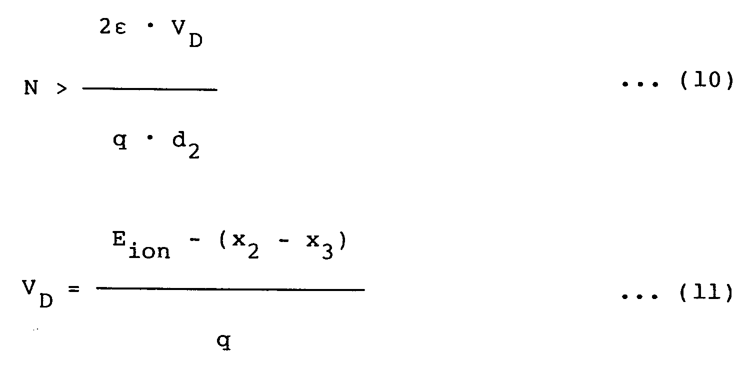
where - ε:
- dielectric constant of impurity layer
- N:
- density of impurity
- x₃:
- electronic affinity of a layer having a maximum forbidden band
- x₂:
- electronic affinity of a layer having a minimum forbidden band
- Eion:
- carrier ionizing energy
- d:
- thickness of impurity layer
- Fig. 7A is a cross sectional structural view which illustrates another embodiment of the photoelectric conversion device according to the present invention, wherein the structure which is formed in the case where the carrier to be multiplied is a positive hole. Referring to Fig. 7A,
reference numeral 602 represents a MOS source or MOS drain serving as a switch device formed on asubstrate Reference numeral 611 represents an electron blocking layer (a charge injection inhibition layer), 612 represents a carrier multiplication portion, 613 represents alight absorption layer, 614 represents a positive hole blocking layer (a charge injection inhibition layer), 616 represents an upper electrode, and 615 represents a passivation layer. Thecarrier multiplication portion 612 is composed of threelayers 612a, 612b and 612c and constituting, together with thelight absorbing layer 613, a photoelectric conversion portion. Furthermore, the layer 612b which constitutes the three-layeredcarrier multiplication portion 612 is formed into a high density p-type layer. - The thickness and the quantity of the added impurities of the impurity additional layer of the hetero junction portion for concentrating the electric field in order to compensate the wanting offset energy may be determined as follows.
- The quantity of impurities to be added is determined to a value with which the voltage to be applied when the impurity layer has been completely depleted is higher than the quantity of the wanting offset energy. That is, it is determined as follows:

where - ε:
- dielectric constant of impurity layer
- N:
- density of impurity
- x₃:
- electronic affinity of a layer having a maximum forbidden band
- x₂:
- electronic affinity of a layer having a minimum forbidden band
- Eion:
- carrier ionizing energy
- d:
- thickness of impurity layer
- Fig. 8 illustrates another embodiment of the photoelectric conversion device according to the present invention, wherein Fig. 8A is a cross sectional structural view, Fig. 8B illustrates an energy band realized when no bias is applied, and Fig. 8C illustrates an energy band realized when a bias required to cause the carrier multiplication to take place.
- In comparison to the energy band of the conventional example shown in Fig. 3, the energy band of the present invention shown in Fig. 8 is different from it in a fact that there is no increase of the energy step due to the application of the bias because the hetero junction portion is not subjected to the impurity doping. The aforesaid fact is a characteristic of the driving method according to the present invention.
- Fig. 9 is a graph which illustrates the characteristics of the APD between electric currents and voltages, the APD having, as the device structure, a carrier multiplication portion composed of three stages. As shown in Fig. 9, with a method of driving the photoelectric conversion device according to the present invention, an electric current corresponding to a quantum efficiency 2 starts passing at a position in the neighborhood of ionization commencement voltage 1Vion1, and then an electric current corresponding to
quantum efficiencies 4 and 8 starts gradually passing at positions in the neighborhood of Vion2 and Vion3. - Fig. 10 illustrates the relationship between inputs and outputs realized when the storage operation is performed by applying a bias higher than Vion3 to the device according to this embodiment. The output is changed in this way that its inclination with respect to the input is changed if it exceeds a certain light quantity to become moderate by a degree corresponding to the step of the current-voltage characteristics until it is saturated. Output saturation characteristics of the aforesaid type can be approximately assumed to be a so-called Knee characteristics with which the dynamic range can be widened. That is, it can be understood that the dynamic range can be widened by a degree (about 8 times according to this embodiment) which equivalents to the multiplication ratio in comparison to the case where the output has no Knee characteristics by superposing the boundary of the subject light quantity region on a point at which the saturation characteristics are commenced.
- Fig. 11 illustrates an example of the structure of a circuit for use in the photoelectric conversion device according to the present invention. Referring to Fig. 11 the charge, which has been generated in a photoelectric conversion device PD before it is multiplied, is divided into a portion to be stored in a capacity CPD of the PD and a portion to be stored in a junction capacity CD of the source portion of the switch MOS transistor TrH. Assuming that the storage time is ts, output voltage ΔV realized when light having a certain light quantity of I is incident can be given from the following equation:

where - q:
- unit charge quantity
- k:
- multiplication constant
- A:
- area of PD
- Assuming that the video bias to be applied to the photoelectric conversion device according to the present invention is VV expressed as follows:

That is, an optimum dynamic range and sensitivity can be obtained by setting VV as follows while assuming that the voltage (voltage with which the multiplication of the electric current is saturated) required for the multiplication to take place in all of n steps of an APD having n-step hetero multiplication portion is Vionmax:

where - Vionmax:
- voltage at which multiplication of current is saturated
- q:
- unit charge quantity
- k:
- multiplication constant
- IKnee:
- light quantity with which Knee characteristics starts taking place
- A:
- area of one pixel
- ts:
- charge storage time
- CPD:
- capacity of photoelectric conversion device portion
- CD:
- storage capacity of switch device
- The quantity of the impurities to be added must be determined to a value with which the voltage which is applied when the impurity layer has been completely depleted made higher than the wanting quantity of the offset energy. That is, it is determined as follows depending upon the fact that the impurity layers are disposed at the two ends of the inclined band gap layer and the fact that the same is disposed at an end of the inclined band gap layer.
- (1) In the case where the impurity layers are present at the two ends of the inclined band gap layer, it is determined by combining the following factors N₁ and N₂:

subscripts 1 and 2 correspond to the wide gap and the narrow gap, ε₁ and ε₂ are dielectric constant, N₁ and N₂ are densities of the impurities, x₁ and x₂ are electronic affinities, Eion is a carrier ionizing energy, and d₁ and d₂ are thicknesses of the impurity layer. In comparison to the aforesaid electron current, the following VD is employed in the case of a positive hole: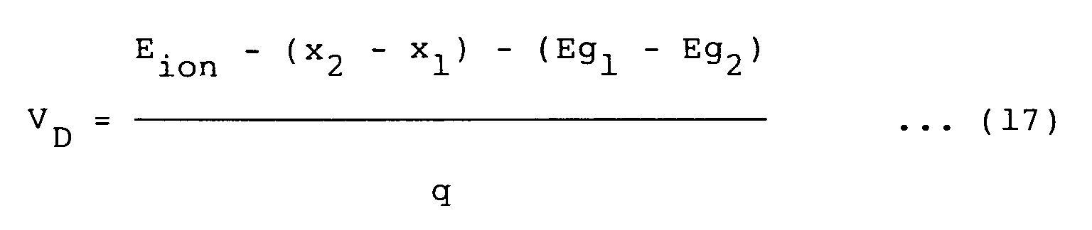
- (2) In the case where the impurity layers are present at the two ends of the inclined band gap layer, the quantity can be determined by the factors expressed as follows:
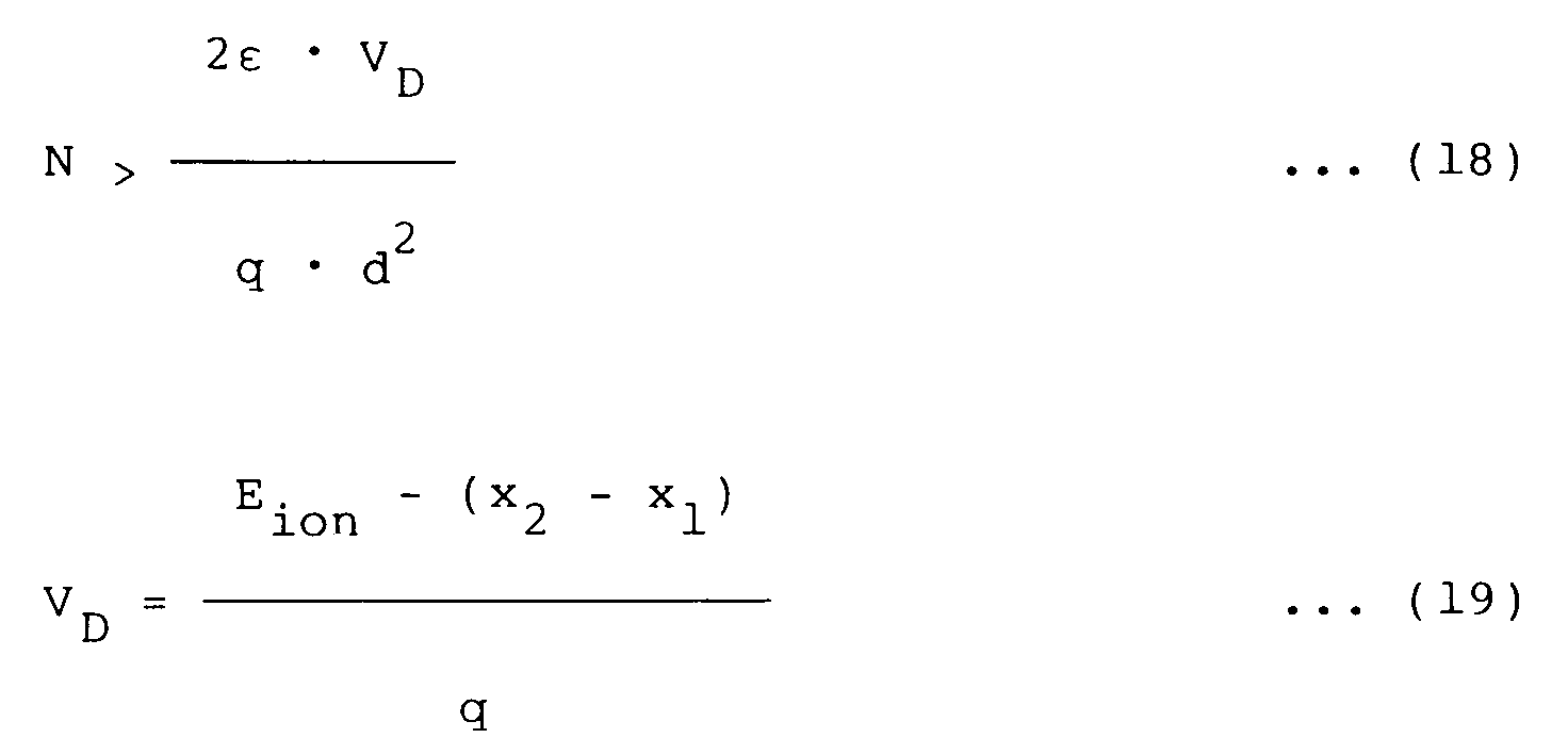
- In comparison to the aforesaid case adapted to the electron current, the quantity in the case of the positive current is determined by the factors expressed as follows:

The bias voltage VV to be applied to the photoelectric conversion device thus manufactured is obtained by using the following parameter in accordance with Equation (21): - Vionmax:
- voltage at which multiplication of the electric current is saturated
- q:
- unit charge quantity
- IKnee:
- light quantity at which Knee characteristics takes place
- A:
- area of one pixel
- ts:
- charge storage time
- k:
- multiplication constant
- CPD:
- capacity of photoelectric conversion device
- CD:
- charge storage capacity of the switch device
- As the substrate for use in the present invention, any one of an insulating substrate, a semiconductor substrate or a metal substrate may be employed if it is able to resist the temperature at the time of the deposition of the films on the substrate, an acid, alkali and a solvent for use to perform the required processes. For example, insulating substrates of a type arranged in such a manner that switch devices and scanning devices are formed on glass, quartz or ceramics are widely used. Also a heat resisting resin film is employed. Semiconductor substrates of a type having a signal processing circuit such as a switch device, an amplifier, and a scanning device are employed. The signal processing circuit is typified by a CCD device, a MOS device, a BBD device and an image sensor disclosed in U.S. Patent No. 4,791,469 and arranged in such a manner that an emitter of a bipolar phototransistor is connected to an output circuit including a capacity load.
- As for the electrode film, either side employs a light transmissive electrode for receiving incidental light, the light transmissive electrode being exemplified by a metal film having a thickness of tens to hundreds of Å and a conductive metal oxide film made of SnO₂, ITO, ZnO₂, IrOx or the like. The residual side is usually made of a metal film which may be selected from a group which meets required conditions such as resistance and chemical properties.
- As the photoconductive film and a carrier multiplication portion, a semiconductor, the valence electron thereof can be controlled, can be employed in the present invention, the semiconductor being exemplified by a tetrahedral (group IV) semiconductor or a composition semiconductor of groups III to V. Semiconductors of group IV are exemplified by Ge, Si, C and their complexes SiGe, SiC, SiGeC, and SiN, SiO and SiSn.
- The i-layer portion (non-dope or a small quantity dope layer) of the semiconductor may be formed into a structure selected from a group consisting of crystal, polycrystal, microcrystal, and amorphous. The term "microcrystal" used hereinbefore is meant a structure containing crystal particles the size of which is tens to hundreds of Å in the amorphous portion thereof and the crystallization rate is raised to tens to 100 %.
- As the impurity to be added for the purpose of controlling the valence electron, a V-group material is used to control the N-type valence electrons, and a III-group material is used to control the P-type valence electrons. Any one of the V-group materials such as P, As, Sb and Bi may be employed, and any one of the III-group materials such as B, Al, Ga, In and Ta may be employed.
- The polycrystal or the microcrystal high density impurity layer may be mainly formed by a CVD method selected from a group consisting of a plasma CVD method, a light CVD method, a heat CVD method, a µW-CVD method, an LP-CVD method, a room pressure CVD method. The crystal particle size is controlled to a size to meet conditions such as the power, the temperature of the substrate, the light quantity, the pressure, and the gas flow rate, and the like (the crystal particle size for determining the conditions is evaluated by an X-ray diffraction method or a direct observation method which uses a TEM).
- The III to V group semiconductors are exemplified by AlGaAsSb, InAsSb, InGaAsSb, InGaAlAs, InAsPSb, InGaAsSb and AlGaP. Any of the materials of group VI such as S, Se, Te and Po may be employed, and any one of the group II materials such as Be, Mg, Ca, Sr, Ba, Ra, Zn, Cd and Hg may be used.
- This embodiment relates to an apparatus having a cross sectional structure formed as shown in Fig. 6A, an energy band profile realized when no bias is applied to the photoelectric conversion device portion and shown in Fig. 6B and an energy band profile realized when a bias required to cause the carrier multiplication to take place and shown in Fig. 6C.
- Figs. 12A to 12F are cross sectional views which illustrates a process of manufacturing the photoelectric conversion device according to the present invention.
- First, the photoelectric conversion device according to this embodiment will now be described with reference to the manufacturing process shown in Figs. 12A to 12F.
- First, a scanning IC substrate comprising a MOS transistor is manufactured by an ordinary MOS processing technology (Fig. 12A).
- Then, the surface of the substrate is flattened for the purpose of stacking the photoelectric conversion device in such a manner that a taking-out
electrode 608 is formed in process (Fig. 12A), and aSiO₂ film 609 is deposited by 8000 Å. Then, an ordinary photoresist is spin-coated so that the surface is flattened before it is etched back by a RIE so as to cause the top portion of theelectrode 608 to appear while maintaining the flatness (Fig. 12B). - Then, Cr is deposited to a thickness of 2000 Å by an ordinary sputtering method, and a desired shape is formed by an ordinary photolithographic process, so that a
pixel electrode 610 is formed (Fig. 12C). Then, the sample is placed in a capacity-coupled plasma CVD apparatus in which a SiH₄ gas and a PH₃ gas diluted to 10 % by a H₂ gas are introduced into the aforesaid apparatus by quantities of 60 SCCM and 20 SCCM respectively so as to perform RF discharge for about 5.5 minutes while making the total gas pressure to be 0.2 Torr. As a result, ahole blocking layer 611 which is an n-type high density layer made of a-Si:H and having a thickness of about 1000 Å is deposited. The temperature of the substrate is 300°C and the density of the discharge power is about 0.2 W/cm² at this time. - Then, in the aforesaid CVD apparatus, the SiH₄ gas is continuously changed from 60 SCCM to 6 SCCM and a GeH₄ gas is continuously changed from 0 SCCM to 54 SCCM in the aforesaid CVD apparatus, and an RF discharge is performed for 2.8 minutes under conditions that the temperature of the substrate is 300°C, the total gas pressure is 0.2 Torr, the RF power density is about 0.5 W/cm², so that an inclined band gap layer 612a made of a-SiGe:H is deposited to have a thickness of about 500 Å (a deposition process 1).
- Then, in the aforesaid CVD apparatus, a 6 SCCM SiH₄ gas, a 54 SCCM GeH₄ gas and a 6 SCCM B₂H₆ gas diluted to 10 % by a H₂ gas are introduced into the aforesaid CVD apparatus and RF discharge is performed for 34 seconds under conditions that the temperature of the substrate is 300°C, the total gas pressure is 0.2 Torr, the RF power density is about 0.5 W/cm², so that a p-type layer 612b made of a-SiGe:H is deposited to have a thickness of about 100 Å (a deposition process 2).
- Then, in the aforesaid CVD apparatus, the flow rate of the SiH₄ gas is gradually changed from 24 SCCM to 60 SCCM and the flow rate of the CH₄ gas is gradually changed from 36 SCCM to 0 SCCM, and RF discharge is performed for about 4.7 minutes seconds under conditions that the temperature of the substrate is 300°C, the total gas pressure is 0.3 Torr, the RF power density is about 0.2 W/cm², so that an inclined
band gap layer 612c made of a-SiC:H is deposited to have a thickness of about 500 Å (a deposition process 3). - Then, the aforesaid deposition processes 1 to 3 are repeated two times, so that three inclined band gap layers are formed.
- Then, in the aforesaid CVD apparatus, the flow rate of the SiH₄ gas is set to 30 SCCM and that of the H₂ gas is set to 30 SCCM, and RF discharge is performed for about 75 minutes under conditions that the temperature of the substrate is 300°C, the total gas pressure is 0.3 Torr, the RF power density is about 0.2 W/cm², so that a light
absorbing layer 613 having a thickness of about 8000 Å is formed. Then, a 24 SCCM SiH₄ gas, a 20 SCCM B₂H₆ gas diluted to 10 % by a H₂ gas and a 36 SCCM CH₄ gas are introduced, and discharge was performed for about 4.7 minutes under the same conditions as those in the deposition process 2, so that ablocking layer 614 having a thickness of about 500 Å is formed (Fig. 12D). - Then, the semiconductor layers 611 to 614 are patterned to be a desired shape and the device was isolated (Fig. 12E).
- Then, the sample is placed in another capacity-coupled plasma CVD apparatus, 10 SCCM of a SiH₄ gas diluted to 10 % by a H₂ gas and 100 SCCM 99.99 % NH₃ gas are introduced, and an RF discharge is performed for about 60 minutes under conditions that the temperature of the substrate is 300°C, the total gas pressure is 0.4 Torr, the RF power density is about 0.01 W/cm², so that a
protection layer 615 having a thickness of about 3000 Å and made of SiHx film is formed. Then, a through hole is formed in theprotection layer 615, and anITO film 616 having a thickness of 700 Å is formed by a sputtering method, so that a photoelectric conversion device is manufactured (Fig. 12F). - In accordance with the aforesaid sequential process, the photoelectric conversion device according to this embodiment is manufactured.
- Figs. 6A to 6C illustrate the photoelectric conversion device according to this embodiment thus manufactured. The device according to this embodiment has a larger energy step in the conductive band in the hetero junction portion with respect to the energy step of the valence electron band and is provided with the
carrier multiplication portion 612 designed to utilize the multiplication of electrons. - Fig. 6B illustrates an energy band of the photoelectric conversion device according to this embodiment thus manufactured. Similarly to Fig. 1 which illustrates the conventional example, symbol Eg₁ represents a required forbidden band, Eg₂ represents a minimum forbidden band, and Eg₃ represents a maximum forbidden band. Symbol V₀ represents energy which is the difference (x₂ - x₃) between electron affinity x₂ of a material of Eg₂ and electron affinity x₃ of a material of Eg₃.
- Although the photoelectric conversion device according to the present invention is structured similarly to the conventional example shown in Fig. 1A in such a manner that the three-step inclined band gap layer forms a hetero junction, the difference lies in that the structure of the conventional example shown in the energy band view shown in Fig. 1A and arranged in such a manner that the Eg₂ portion is made of an n-type structure and the Eg₃ portion is made of an i-type structure is replaced by a structure arranged in such a manner that the Eg₂ portion is made of a p-type structure and the Eg₃ portion is made of an i-type structure. The aforesaid structure is a characteristic of this embodiment.
- Fig. 6C illustrates an energy band realized when a bias is applied. As can be seen from this, an electric field acting on the light absorbing portion Eg₁ is relatively weakened and an effect can be obtained in that the bias required to be applied to the overall portion of the device can be reduced.
- Fig. 13 is a graph which illustrates the characteristics of the APD between electric currents and voltages, the APD having the three-step carrier multiplication portion as shown in Figs. 6A to 6C. As shown in Fig. 13, an electric current corresponding to a quantum efficiency 2 starts passing at a position in the neighborhood exceeding ionization commencement voltage 1Vion1, and then an electric current corresponding to
quantum efficiencies 4 and 8 starts gradually passing at positions in the neighborhood of Vion2 and Vion3. - Fig. 14 illustrates the relationship between inputs and outputs realized when the storage operation is performed by applying a bias higher than Vion3 to the device according to this embodiment. The output is, as shown in Fig. 14, changed in this way that its inclination with respect to the input is changed if it exceeds a certain light quantity to become moderate by a degree corresponding to the step of the current-voltage characteristics until it is saturated. An output saturation characteristics of the aforesaid type can be approximately assumed to be a so-called Knee characteristics with which the dynamic range can be widened.
- That is, it can be understood that the dynamic range can be widened by a degree (about 8 times according to this embodiment) which equivalents to the multiplication ratio in comparison to the case where the output has no Knee characteristics by superposing the boundary of the subject light quantity region on a point at which the saturation characteristics are commenced.
- Then, a method of driving the photoelectric conversion device according to this embodiment and thus manufactured with a minimum voltage level will now be described.
- As described above, the bias voltage VV to be applied to the two ends of the light absorbing layer and the carrier multiplication layer of the photoelectric conversion device must meet the following relationship:

where - EC OFF:
- energy step of the conductive band in the hetero junction portion in which the forbidden band is discontinuously changed from the maximum value to the minimum value
- dP:
- thickness of light absorbing layer
- dA:
- thickness of carrier multiplication layer
- dGRD int:
- thickness of one inclined band gap layer
- dEG2 dop:
- thickness of one layer having the maximum forbidden band to which impurities are added to a high density
- n:
- number of hetero junction portions of layer having the maximum forbidden band and a layer having the minimum forbidden band
- Substituting the aforesaid parameters to aforesaid Equation (22), the following result is obtained:

Therefore, the aforesaid equation can be met if 30 V is applied as the bias voltage (video voltage). - When a video voltage VV of 30 V was added to the photoelectric conversion device thus manufactured while making the voltage level at the light absorbing layer to be lower than that at the carrier multiplication layer, the Knee characteristics took place in the output in the neighborhood of a surface illuminance of the photoelectric conversion device of about 300 lux, and it was saturated at about 2000 lux, and a dynamic range of about 95 dB was obtained.
- A sensitivity of 8 times the sensitivity, which was realized when an ordinary PN, PIN, or shot key device was used, was obtained. Thus, excellent sensitivity and wide dynamic range were realized.
- As described above, according to the present invention, the Knee characteristics can be attained in the charge storage operation, the dynamic range can be widened, and excellent sensitivity can be realized since the photoelectric conversion device, on which the APD arranged to utilize the electron multiplication and having a structure formed by repeating the inclined band gap is mounted, is arranged in such a manner that at least a portion having the minimum forbidden width Eg₂ of the hetero junction portion of the minimum forbidden band Eg₂ portion of the inclined band gap layer and the maximum forbidden band Eg₃ portion of the other inclined band gap layer is made to be a high density P-type semiconductor layer.
- Furthermore, the photoelectric conversion device can be driven by a voltage level lower than that required in the conventional example by making the bias voltage VV to be added to the device to be lower in the light absorbing layer than that to be applied to the carrier multiplication layer while meeting the conditional equation.
- This embodiment relates to an apparatus having a cross sectional structure formed as shown in Fig. 8A, an energy band profile realized when no bias is applied to the photoelectric conversion device portion and shown in Fig. 8B and an energy band profile realized when a bias required to cause the carrier multiplication to take place and shown in Fig. 8C.
- Figs. 15A to 15F are cross sectional views which illustrate a process of manufacturing the photoelectric conversion device according to the present invention.
- First, the photoelectric conversion device according to this embodiment will now be described with reference to the manufacturing process shown in Figs. 15A to 15F.
- First, a scanning IC substrate comprising a MOS transistor is manufactured by an ordinary MOS processing technology (Fig. 12A).
- Then, the surface of the substrate is flattened for the purpose of stacking the photoelectric conversion device in such a manner that a taking-out
electrode 608 is formed in process (Fig. 12A), and aSiO₂ film 609 is deposited by 8000 Å. Then, an ordinary photoresist is spin-coated so that the surface is flattened before it is etched back by a RIE so as to cause the top portion of theelectrode 608 to appear while maintaining the flatness (Fig. 12B). - Then, Cr is deposited to a thickness of 2000 Å by an ordinary sputtering method, and a desired shape is formed by an ordinary photolithographic process, so that a
pixel electrode 610 is formed (Fig. 12C). Then, the sample is placed in a capacity-coupled plasma CVD apparatus in which a SiH₄ gas and a B₂H₆ gas diluted to 10 % by a H₂ gas are introduced into the aforesaid apparatus by quantities of 60 SCCM and 20 SCCM respectively so as to perform RF discharge for about 5.5 minutes while making the total gas pressure to be 0.2 Torr. As a result, anelectron blocking layer 611 which is a p-type high density layer made of a-Si:H and having a thickness of about 1000 Å is deposited. The temperature of the substrate is 300°C and the density of the discharge power is about 0.2 W/cm² at this time. - Then, in the aforesaid CVD apparatus, the SiH₄ gas is continuously changed from 60 SCCM to 6 SCCM and a GeH₄ gas is continuously changed from 0 SCCM to 54 SCCM in the aforesaid CVD apparatus, and an RF discharge is performed for 2.8 minutes under conditions that the temperature of the substrate is 300°C, the total gas pressure is 0.2 Torr, the RF power density is about 0.5 W/cm², so that an inclined band gap layer 612a made of a-SiGe:H is deposited to have a thickness of about 500 Å (a deposition process 1).
- Then, in the aforesaid CVD apparatus, a 6 SCCM SiH₄ gas, a 54 SCCM GeH₄ gas and a 6 SCCM PH₃ gas diluted to 10 % by a H₂ gas are introduced into the aforesaid CVD apparatus and RF discharge is performed for 34 seconds under conditions that the temperature of the substrate is 300°C, the total gas pressure is 0.2 Torr, the RF power density is about 0.5 W/cm², so that a n-type layer 612b made of a-SiGe:H is deposited to have a thickness of about 100 Å (a deposition process 2).
- Then, in the aforesaid CVD apparatus, the flow rate of the SiH₄ gas is gradually changed from 24 SCCM to 60 SCCM and the flow rate of the NH₃ gas is gradually changed from 36 SCCM to 0 SCCM, and RF discharge is performed for about 4.7 minutes under conditions that the temperature of the substrate is 300°C, the total gas pressure is 0.3 Torr, the RF power density is about 0.2 W/cm², so that an inclined
band gap layer 612c made of a-SiN:H is deposited to have a thickness of about 500 Å (a deposition process 3). - Then, the aforesaid deposition processes 1 to 3 are repeated two times, so that three inclined band gap layers are formed.
- Then, in the aforesaid CVD apparatus, the flow rate of the SiH₄ gas is set to 30 SCCM and that of the H₂ gas is set to 30 SCCM, and RF discharge is performed for about 75 minutes under conditions that the temperature of the substrate is 300°C, the total gas pressure is 0.3 Torr, the RF power density is about 0.2 W/cm², so that a light
absorbing layer 613 having a thickness of about 8000 Å is formed. Then, a 24 SCCM SiH₄ gas, a 20 SCCM PH₃ gas diluted to 10 % by a H₂ gas and a 36 SCCM NH₃ gas are introduced, and discharge was performed for about 4.7 minutes under the same conditions as those in the deposition process 3, so that ablocking layer 614 having a thickness of about 500 Å is formed (Fig. 12D). - Then, the semiconductor layers 611 to 614 are patterned to be a desired shape and the device was isolated (Fig. 12E).
- Then, the sample is placed in another capacity-coupled plasma CVD apparatus, 10 SCCM of a SiH₄ gas diluted to 10 % by a H₂ gas and 100 SCCM 99.99 % NH₃ gas are introduced, and an RF discharge is performed for about 60 minutes under conditions that the temperature of the substrate is 300°C, the total gas pressure is 0.4 Torr, the RF power density is about 0.01 W/cm², so that a
protection layer 615 having a thickness of about 3000 Å and made of SiHx film is formed. Then, a through hole is formed in theprotection layer 615, and anITO film 616 having a thickness of 700 Å is formed by a sputtering method, so that a photoelectric conversion device is manufactured (Fig. 12F). - In accordance with the aforesaid sequential process, the photoelectric conversion device according to this embodiment is manufactured.
- Figs. 7A to 7C illustrate the photoelectric conversion devices according to this embodiment thus manufactured. The device according to this embodiment has a larger energy step in the valence electron band in the hetero junction portion with respect to the energy step in the conductive band and is provided with the
carrier multiplication portion 612 designed to utilize the multiplication of electrons. - Fig. 7B illustrates an energy band of the photoelectric conversion device according to this embodiment thus manufactured. Symbol Eg₁ represents a required forbidden band, Eg₂ represents a minimum forbidden band, and Eg₃ represents a maximum forbidden band. Symbol V₀ represents energy which is the difference (x₂ - x₃) between electron affinity x₂ of a material of Eg₂ and electron affinity x₃ of a material of Eg₃.
- Although the photoelectric conversion device according to the present invention is structured similarly to the comparative example shown in Figs. 16A to 16C in such a manner that the three-step inclined band gap layer forms a hetero junction, the difference lies in that the structure of the comparative example shown in the energy band view shown in Fig. 16A and arranged in such a manner that the Eg₂ portion is made of a p-type structure and the Eg₃ portion is made of an i-type structure is replaced by a structure arranged in such a manner that the Eg₂ portion is made of a n-type structure and the Eg₃ portion is made of an i-type structure. The aforesaid structure is a characteristic of this embodiment.
- Fig. 7C illustrates an energy band realized when a bias is applied. As can be seen from this, an electric field acting on the light absorbing portion Eg₁ is relatively weakened and an effect can be obtained in that the bias required to be applied to the overall portion of the device can be reduced.
- Fig. 17 is a graph which illustrates the characteristics of the APD between electric currents and voltages, the APD having the three-step carrier multiplication portion as shown in Figs. 7A to 7C. As shown in Fig. 17, an electric current corresponding to a quantum efficiency 2 starts passing at a position in the neighborhood exceeding ionization commencement voltage 1Vion1, and then an electric current corresponding to
quantum efficiencies 4 and 8 starts gradually passing at positions in the neighborhood of Vion2 and Vion3. - Fig. 18 illustrates the relationship between inputs and outputs realized when the storage operation is performed by applying a bias higher than Vion3 to the device according to this embodiment. The output is, as shown in Fig. 18, changed in this way that its inclination with respect to the input is changed if it exceeds a certain light quantity to become moderate by a degree corresponding to the step of the current-voltage characteristics until it is saturated. An output saturation characteristics of the aforesaid type can be approximately assumed to be a so-called Knee characteristics with which the dynamic range can be widened.
- That is, it can be understood that the dynamic range can be widened by a degree (about 8 times according to this embodiment) which equivalents to the multiplication ratio in comparison to the case where the output has no Knee characteristics by superposing the boundary of the subject light quantity region on a point at which the saturation characteristics are commenced.
- Then, a method of driving the photoelectric conversion device according to this embodiment and thus manufactured with a minimum voltage level will now be described.
- As described above, the bias voltage VV to be applied to the two ends of the light absorbing layer and the carrier multiplication layer of the photoelectric conversion device must meet the following relationship:
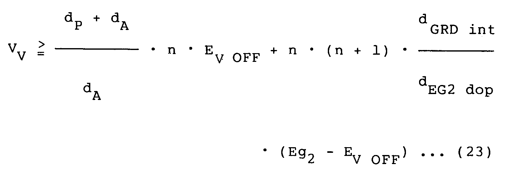
where - EV OFF:
- energy step of the valence electron band in the hetero junction portion in which the forbidden band is discontinuously changed from the maximum value to the minimum value
- dP:
- thickness of light absorbing layer
- dA:
- thickness of carrier multiplication layer
- dGRD int:
- thickness of one inclined band gap layer
- dEG2 dop:
- thickness of one layer having the maximum forbidden band to which impurities are added to a high density
- n:
- number of herero junction portions of a layer having the maximum forbidden band and a layer having the minimum forbidden band
- When a video voltage VV of 30V was added to the photoelectric conversion device thus manufactured while making the voltage level at the light absorbing layer to be lower than that at the carrier multiplication layer, the Knee characteristics took place in the output in the neighborhood of a surface illuminance of the photoelectric conversion device of about 300 lux, and it was saturated at about 2000 lux, and a dynamic range of about 95 dB was obtained.
- A sensitivity of 8 times the sensitivity, which was realized when an ordinary PN, PIN, or shot key device was used, was obtained. Thus, excellent sensitivity and wide dynamic range were realized.
- As described above, according to the present invention, the Knee characteristics can be attained in the charge storage operation, the dynamic range can be widened, and excellent sensitivity can be realized since the photoelectric conversion device, on which the APD arranged to utilize the electron multiplication and having a structure formed by repeating the inclined band gap is mounted, is arranged in such a manner that at least a portion having the minimum forbidden width Eg₂ of the hetero junction portion of the minimum forbidden band Eg₂ portion of the inclined band gap layer and the maximum forbidden band Eg₃ portion of the other inclined band gap layer is made to be a high density n-type semiconductor layer.
- Furthermore, the photoelectric conversion device can be driven by a voltage level lower than that required in the conventional example by making the bias voltage VV to be added to the device to be lower in the light absorbing layer than that to be applied to the carrier multiplication layer while meeting the conditional equation.
- This embodiment relates to an apparatus having a cross sectional structure formed as shown in Fig. 8A, an energy band profile realized when no bias is applied to the photoelectric conversion device portion and shown in Fig. 8B and an energy band profile realized when a bias required to cause the carrier multiplication to take place and shown in Fig. 8C.
- Figs. 19A to 19F are cross sectional views which illustrates a process of manufacturing the photoelectric conversion device according to the present invention. First, the photoelectric conversion device according to this embodiment will now be described with reference to the manufacturing process shown in Figs. 12A to 12F.
- First, a scanning IC substrate comprising a MOS transistor is manufactured by ordinary MOS processing technology (Fig. 19A).
- Then, the surface of the substrate is flattened for the purpose of stacking the photoelectric conversion device in such a manner that a taking-out
electrode 908 is formed in process (Fig. 19A), aSiO₂ film 909 is deposited by 8000 Å. Then, an ordinary photoresist is spin-coated so that the surface is flattened before it is etched back by a RIE so as to cause the top portion of theelectrode 908 to appear while maintaining the flatness (Fig. 19B). - Then, Cr is deposited to a thickness of 2000 Å by an ordinary sputtering method, and a desired shape is formed by an ordinary photolithographic process, so that a
pixel electrode 910 is formed (Fig. 19C). Then, the sample is placed in a capacity-coupled plasma CVD apparatus in which a 65 CCM SiH₄ gas, a 54 SCCM GeH₄ gas, and 20 SCCM PH₃ gas diluted to 10 % by a H₂ gas are introduced into the aforesaid apparatus so as to perform RF discharge for about 5.5 minutes while making the total gas pressure to be 0.2 Torr. As a result, ahole blocking layer 911 which is an n-type high density layer made of a-SiGe:H and having a thickness of about 1000 Å is deposited. The temperature of the substrate is 300°C and the density of the discharge power is about 0.2 W/cm² at this time. - Then, in the aforesaid CVD apparatus, the SiH₄ gas is continuously changed from 60 SCCM to 6 SCCM and a GeH₄ gas is continuously changed from 0 SCCM to 54 SCCM in the aforesaid CVD apparatus, and an RF discharge is performed for 2.8 minutes under conditions that the temperature of the substrate is 300°C, the total gas pressure is 0.2 Torr, the RF power density is about 0.5 W/cm², so that an inclined
band gap layer 912a made of a-SiGe:H is deposited to have a thickness of about 500 Å (a deposition process 1). - Then, in the aforesaid CVD apparatus, a 24 SCCM SiH₄ gas, a 36 SCCM CH₄ gas, and a 6 SCCM B₂H₆ gas diluted to 10 % by a H₂ gas are introduced into the aforesaid CVD apparatus and RF discharge is performed for 56 seconds under conditions that the temperature of the substrate is 300°C, the total gas pressure is 0.3 Torr, the RF power density is about 0.2 W/cm², so that a p-type layer 912b made of a-SiC:H is deposited to have a thickness of about 100 Å (a deposition process 2).
- Then, in the aforesaid CVD apparatus, the flow rate of the SiH₄ gas is gradually changed from 24 SCCM to 60 SCCM and the flow rate of the CH₄ gas is gradually changed from 36 SCCM to 0 SCCM, and RF discharge is performed for about 4.7 minutes seconds under conditions that the temperature of the substrate is 300°C, the total gas pressure is 0.3 Torr, the RF power density is about 0.2 W/cm², so that an inclined
band gap layer 912c made of a-SiC:H is deposited to have a thickness of about 500 Å (a deposition process 3). - Then, the aforesaid deposition processes 1 to 3 are repeated two times, so that three inclined band gap layers are formed.
- Then, in the aforesaid CVD apparatus, the flow rate of the SiH₄ gas is set to 30 SCCM and that of the H₂ gas is set to 30 SCCM, and RF discharge is performed for about 75 minutes under conditions that the temperature of the substrate is 300°C, the total gas pressure is 0.3 Torr, the RF power density is about 0.2 W/cm², so that a light
absorbing layer 913 having a thickness of about 8000 Å is formed. Then, a 24 SCCM SiH₄ gas, a 20 SCCM B₂H₆ gas diluted to 10 % by a H₂ gas and a 36 SCCM CH₄ gas are introduced, and discharge was performed for about 5 minutes under the same conditions as those in the deposition process 2, so that ablocking layer 914 having a thickness of about 500 Å is formed (Fig. 19D). - Then, the semiconductor layers 911 to 914 are patterned to be a desired shape and the device was isolated (Fig. 19E).
- Then, the sample is placed in another capacity-coupled plasma CVD apparatus, 10 SCCM of a SiH₄ gas diluted to 10 % by a H₂ gas and 100 SCCM 99.99 % NH₃ gas are introduced, and an RF discharge is performed for about 60 minutes under conditions that the temperature of the substrate is 300°C, the total gas pressure is 0.4 Torr, the RF power density is about 0.01 W/cm², so that a
protection layer 915 having a thickness of about 3000 Å and made of SiHx film is formed. Then, a through hole is formed in theprotection layer 915, and anITO film 916 having a thickness of 700 Å is formed by a sputtering method, so that a photoelectric conversion device is manufactured (Fig. 19F). - In accordance with the aforesaid sequential process, the photoelectric conversion device according to this embodiment is manufactured.
- In order to perform the driving method according to the present invention, the following relation equation for obtaining the bias VV to be applied to the aforesaid photoelectric conversion device is employed:

where - Vionmax:
- voltage at which multiplication of current is saturated
- q:
- unit charge quantity
- k:
- multiplication constant
- IKnee:
- light quantity with which Knee characteristics take place
- A:
- area of one pixel
- ts:
- charge storage time
- CPD:
- capacity of photoelectric conversion device portion
- CD:
- capacity stored in switch device
- A sensitivity of 8 times the sensitivity, which was realized when an ordinary PN, PIN, or shot key device was used, was obtained. Thus, excellent sensitivity and wide dynamic range were realized.
- As described above, according to the present invention, the method of driving the photoelectric conversion device having a repeated structure of inclined band gap layers is arranged in such a manner that voltage VV which meets the following relationship is applied to the aforesaid photoelectric conversion device:

so that an effect is obtained in that a large dynamic range can be maintained while preventing deterioration of the S/N ratio. - Fig. 20 is a block diagram which illustrates a control system of an information signal processing system having the photoelectric conversion device according to the present invention and shown in Fig. 11. A control circuit COUT transmits pulses φ1, φ2, φSH and φSV and receives a signal SOUT. The image signal SOUT is A/D-converted, and is stored in a memory MEMO. The aforesaid signal is read from the memory MEMO if necessary and is recorded on a recording medium by using a recording head HD. Symbol DRV represents a drive circuit for driving the recording head.
- A photoelectric conversion device including: a photoelectric conversion portion having a light absorbing layer disposed between charge injection inhibition layers and having a predetermined forbidden band width Eg₁, and a carrier multiplication portion including a single or a plurality of inclined band gap layers, the inclined band gap layer including a minimum forbidden band width Eg₂ and a maximum forbidden band width Eg₃ which are disposed to be in contact with each other to form a hetero junction and having, at the two ends thereof, forbidden band widths Eg₄ which holds a relationship Eg₂ < Eg₄ < Eg₃ in such a manner that the forbidden band width is continuously changed from the two forbidden band widths Eg₂ and Eg₃ to the forbidden band width Eg₄, and the energy step in a conductive band of the hetero junction portion is larger than the energy step in a valence electron band, wherein at least the minimum forbidden band width Eg₂ of portions which form the hetero junction is made of a high density p-type semiconductor.

The electric field intensity EDK acting at the end of each impurity layer is expressed by:

Since also the aforesaid electric field is applied to the k-th inclined band gap layer, the voltage VAI to be applied to all of the inclined band gap layer is expressed by:

The impurity density NI is set by the following equation:

Assuming that the voltage required to deplete the inclined gap layer is superposed prior to the depletion of the impurity layer, the voltage corresponding to the superposed portion can be obtained as follows:
The voltage VAI DEP for the multiplication layer is given by:
The voltage VP DEP to be distributed to the light absorbing layer is given by:
Therefore, overall voltage VDEP is given by:
As a result, the voltage VV to be applied to the device is the sum of (1), (2) and (3). However, it can be considered that the portion of (1) is small. A value given from the following equation may be added to obtain the minimum driving voltage:
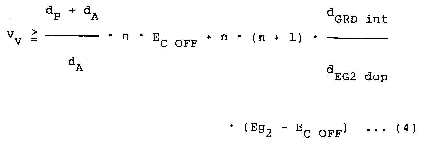
Therefore, a photoelectric conversion device which has the Knee characteristics in the charge storage operation and which can be driven by a low voltage can be provided.

The electric field intensity EDk acting at the end of each impurity layer is expressed by:

Since also the aforesaid electric field is applied to the k-th inclined band gap layer, the voltage VAI to be applied to all of the inclined band gap layer is expressed by:

The impurity density NI is set by the following equation:

Assuming that the voltage required to deplete the inclined gap layer is superposed prior to the depletion of the impurity layer, the voltage corresponding to the superposed portion can be obtained as follows:
The voltage VAI DEP for the multiplication layer is given by:
The voltage VP DEP to be distributed to the light absorbing layer is given by:
Therefore, overall voltage VDEP is given by:
As a result, the voltage VV to be applied to the device is the sum of (5), (6) and (7). However, it can be considered that the portion of (5) is small. A value given from the following equation may be added to obtain the minimum driving voltage:

As a result, according to the present invention, there is provided a photoelectric conversion device which has the Knee characteristics in the charge storage operation and which can be drive by low voltage.
By applying VV thus obtained, the photoelectric conversion device can be driven by a lower voltage level in comparison to the conventional technology.
dP = 8000 Å
dA = 3000 Å
dGRD int= 1000 Å
dEG2 dop = 100 Å
n = 3.
dP = 8000 Å
dA = 3000 Å
dGRD int = 1000 Å
dEG2 dop = 100 Å
n = 3
Substituting the aforesaid parameters to aforesaid Equation (23), the following result is obtained:

Therefore, the aforesaid equation can be met if 30 V is applied as the bias voltage (video voltage).

When a video voltage VV of 30 V was, as the applied bias voltage (video voltage), added to the photoelectric conversion device thus manufactured while making the voltage level at the light absorbing layer to be lower than that at the carrier multiplication layer, the Knee characteristics took place in the output in the neighborhood of a surface illuminance of the photoelectric conversion device of about 300 lux, and it was saturated at about 2000 lux, and a dynamic range of about 95 dB was obtained.
Claims (7)
- A photoelectric conversion device comprising:
a photoelectric conversion portion having
a light absorbing layer disposed between charge injection inhibition layers and having a predetermined forbidden band width Eg₁, and
a carrier multiplication portion including a single or a plurality of inclined band gap layers,
said inclined band gap layer including a minimum forbidden band width Eg₂ and a maximum forbidden band width Eg₃ which are disposed to be in contact with each other to form a hetero junction and having, at the two ends thereof, forbidden band widths Eg₄ which holds a relationship Eg₂ < Eg₄ < Eg₃ in such a manner that the forbidden band width is continuously changed from said two forbidden band widths Eg₂ and Eg₃ to said forbidden band width Eg₄, and the energy step in a conductive band of said hetero junction portion is larger than the energy step in a valence electron band, wherein
at least said minimum forbidden band width Eg₂ of portions which form said hetero junction is made of a high density p-type semiconductor. - A method of driving a photoelectric conversion device according to claim 1, wherein said photoelectric conversion device is driven by bias voltage VV applied to the two ends of said light absorbing layer and said carrier multiplication portion of said photoelectric conversion device in such a manner that the potential of said bias voltage VV applied to said light absorbing layer is lower than that applied to said carrier multiplication layer.
- A method of driving a photoelectric conversion device according to claim 2, wherein said photoelectric conversion device is driven by said bias voltage VV applied to the two ends of said light absorbing layer and said carrier multiplication portion of said photoelectric conversion device, said bias voltage VV holding the following relationship:
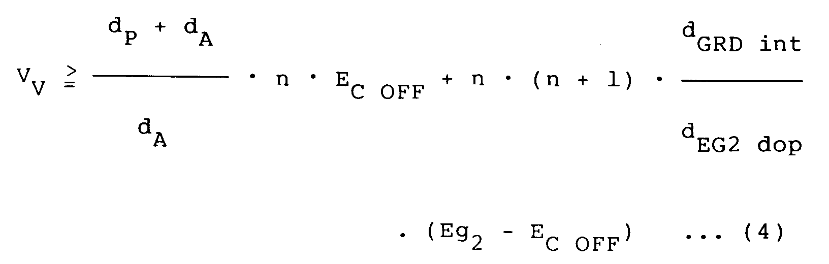 EC OFF: energy step of the conductive band in the hetero junction portion in which the forbidden band is discontinuously changed from the maximum value to the minimum valuedP: thickness of light absorbing layerdA: thickness of carrier multiplication layerdGRD int: thickness of one inclined band gap layerdEG2 dop: thickness of one layer having the maximum forbidden band to which impurities are added to a high densityn: number of hetero junction portions of a layer having the maximum forbidden band and a layer having the minimum forbidden band.
 - A photoelectric conversion device comprising:
a photoelectric conversion portion having
a light absorbing layer disposed between charge injection inhibition layers and having a predetermined forbidden band width Eg₁, and
a carrier multiplication portion including a single or a plurality of inclined band gap layers,
said inclined band gap layer including a minimum forbidden band width Eg₂ and a maximum forbidden band width Eg₃ which are disposed to be in contact with each other to form a hetero junction and having, at the two ends thereof, forbidden band widths Eg₄ which holds a relationship Eg₂ < Eg₄ < Eg₃ in such a manner that the forbidden band width is continuously changed from said two forbidden band widths Eg₂ and Eg₃ to said forbidden band width Eg₄, and the energy step in a conductive band of said hetero junction portion is larger than the energy step in a valence electron band, wherein
at least said minimum forbidden band width Eg₂ of portions which form said hetero junction is made of a high density n-type semiconductor. - A method of driving a photoelectric conversion device according to claim 4, wherein said photoelectric conversion device is driven by bias voltage VV applied to the two ends of said light absorbing layer and said carrier multiplication portion of said photoelectric conversion device in such a manner that the potential of said bias voltage VV applied to said light absorbing layer is lower than that applied to said carrier multiplication layer.
- A method of driving a photoelectric conversion device according to claim 2, wherein said photoelectric conversion device is driven by said bias voltage VV applied to the two ends of said light absorbing layer and said carrier multiplication portion of said photoelectric conversion device, said bias voltage VV holding the following relationship:
 EV OFF: energy step of a valence band in the hetero junction portion in which the forbidden band is discontinuously changed from the maximum value to the minimum valuedP: thickness of light absorbing layerdA: thickness of carrier multiplication layerdGRD int: thickness of one inclined band gap layerdEG2 dop: thickness of one layer having the maximum forbidden band to which impurities are added to a high densityn: number of hetero junction portions of a layer having the maximum forbidden band and a layer having the minimum forbidden band.
 - A method of driving a photoelectric conversion device which has a photoelectric conversion portion composed of
a light absorbing layer disposed between charge injection inhibition layers and having a predetermined forbidden band width Eg₁, and
a carrier multiplication layer connected to a switch device, said carrier multiplication portion having at least one layer formed into a step back structure which has minimum forbidden band widths Eg₂ and maximum forbidden band widths Eg₃ disposed alternately and in which said forbidden band width is continuously changed between said two forbidden bands, and arranged in such a manner that impurities are added to at least a layer having said minimum forbidden band width Eg₂ or a layer having said maximum forbidden band width Eg₃, said method of driving a photoelectric conversion device comprising the step of:
driving said photoelectric conversion device by applying bias VV to said photoelectric conversion device, said bias VV being arranged to meet the following equation:

whereVionmax: voltage at which multiplication of current is saturatedq: unit charge quantityk: multiplication constantIKnee: light quantity with which Knee characteristics starts taking placeA: area of one pixelts: charge storage timeCPD: capacity of photoelectric conversion device portionCD: storage capacity of switch device.
Applications Claiming Priority (9)
| Application Number | Priority Date | Filing Date | Title |
|---|---|---|---|
| JP332787/91 | 1991-11-22 | ||
| JP33278591 | 1991-11-22 | ||
| JP33278791 | 1991-11-22 | ||
| JP332786/91 | 1991-11-22 | ||
| JP3332786A JPH05145109A (en) | 1991-11-22 | 1991-11-22 | Photoelectric conversion device and driving method thereof |
| JP3332787A JPH05145110A (en) | 1991-11-22 | 1991-11-22 | Photoelectric conversion device and driving method thereof |
| JP332785/91 | 1991-11-22 | ||
| JP3332785A JPH05145108A (en) | 1991-11-22 | 1991-11-22 | Drive method of photoconversion device |
| JP33278691 | 1991-11-22 |
Publications (3)
| Publication Number | Publication Date |
|---|---|
| EP0543391A2 true EP0543391A2 (en) | 1993-05-26 |
| EP0543391A3 EP0543391A3 (en) | 1994-04-27 |
| EP0543391B1 EP0543391B1 (en) | 2000-08-30 |
Family
ID=27340561
Family Applications (1)
| Application Number | Title | Priority Date | Filing Date |
|---|---|---|---|
| EP92119795A Expired - Lifetime EP0543391B1 (en) | 1991-11-22 | 1992-11-20 | Photoelectric conversion device and method of driving the same |
Country Status (3)
| Country | Link |
|---|---|
| US (1) | US5767560A (en) |
| EP (1) | EP0543391B1 (en) |
| DE (1) | DE69231398T2 (en) |
Families Citing this family (8)
| Publication number | Priority date | Publication date | Assignee | Title |
|---|---|---|---|---|
| US5993627A (en) * | 1997-06-24 | 1999-11-30 | Large Scale Biology Corporation | Automated system for two-dimensional electrophoresis |
| US6353250B1 (en) * | 1997-11-07 | 2002-03-05 | Nippon Telegraph And Telephone Corporation | Semiconductor photo-detector, semiconductor photo-detection device, and production methods thereof |
| US6252221B1 (en) * | 1999-06-21 | 2001-06-26 | Agilent Technologies, Inc. | Photo-conductive switch having an improved semiconductor structure |
| US6229202B1 (en) | 2000-01-10 | 2001-05-08 | Micron Technology, Inc. | Semiconductor package having downset leadframe for reducing package bow |
| US20020130311A1 (en) * | 2000-08-22 | 2002-09-19 | Lieber Charles M. | Doped elongated semiconductors, growing such semiconductors, devices including such semiconductors and fabricating such devices |
| WO2004079311A1 (en) * | 2003-03-07 | 2004-09-16 | Fujitsu Limited | Electromagnetic radiation sensor and method for fabricating the same |
| US8239176B2 (en) * | 2008-02-13 | 2012-08-07 | Feng Ma | Simulation methods and systems for carriers having multiplications |
| JP6145655B2 (en) | 2012-12-18 | 2017-06-14 | パナソニックIpマネジメント株式会社 | Semiconductor photodetector |
Family Cites Families (8)
| Publication number | Priority date | Publication date | Assignee | Title |
|---|---|---|---|---|
| US4476477A (en) * | 1982-02-23 | 1984-10-09 | At&T Bell Laboratories | Graded bandgap multilayer avalanche photodetector with energy step backs |
| US4686554A (en) * | 1983-07-02 | 1987-08-11 | Canon Kabushiki Kaisha | Photoelectric converter |
| US4886977A (en) * | 1986-11-11 | 1989-12-12 | Canon Kabushiki Kaisha | Photoelectric converter provided with voltage dividing means |
| US5019887A (en) * | 1987-03-27 | 1991-05-28 | Canon Kabushiki Kaisha | Non-single crystalline photosensor with hydrogen and halogen |
| JPH0715979B2 (en) * | 1987-08-27 | 1995-02-22 | 三菱電機株式会社 | Superlattice image sensor |
| JPH02275670A (en) * | 1989-01-18 | 1990-11-09 | Canon Inc | Photoelectric converter and image reader |
| DE69033657T2 (en) * | 1989-08-04 | 2001-05-03 | Canon K.K., Tokio/Tokyo | PHOTOELECTRIC CONVERTER |
| EP0444963B1 (en) * | 1990-03-02 | 1997-09-17 | Canon Kabushiki Kaisha | Photoelectric transfer device |
-
1992
- 1992-11-20 EP EP92119795A patent/EP0543391B1/en not_active Expired - Lifetime
- 1992-11-20 DE DE69231398T patent/DE69231398T2/en not_active Expired - Fee Related
-
1994
- 1994-11-30 US US08/352,688 patent/US5767560A/en not_active Expired - Fee Related
Also Published As
| Publication number | Publication date |
|---|---|
| EP0543391A3 (en) | 1994-04-27 |
| US5767560A (en) | 1998-06-16 |
| EP0543391B1 (en) | 2000-08-30 |
| DE69231398D1 (en) | 2000-10-05 |
| DE69231398T2 (en) | 2001-02-22 |
Similar Documents
| Publication | Publication Date | Title |
|---|---|---|
| EP0538886B1 (en) | Signal processor having avalanche photodiodes | |
| JP3645585B2 (en) | Charge coupled device type solid-state imaging device having overflow drain structure | |
| EP0542152B1 (en) | Laminated solid-state image sensing apparatus and method of manufacturing the same | |
| US4862237A (en) | Solid state image sensor | |
| EP0488174B1 (en) | Photoelectric converting device and information processing apparatus employing the same | |
| US5273910A (en) | Method of making a solid state electromagnetic radiation detector | |
| EP0214408B1 (en) | Solid-state image sensor | |
| EP0186162B1 (en) | Solid state image sensor | |
| US5084747A (en) | Photoelectric conversion device having cells of different spectral sensitivities | |
| JPH0410785B2 (en) | ||
| US4462047A (en) | Solid state imager with blooming suppression | |
| CA1096498A (en) | Ccd radiation sensor | |
| JPH05211321A (en) | Avalanche photodiode and signal processing device using thereof | |
| EP0543391B1 (en) | Photoelectric conversion device and method of driving the same | |
| JPH0513748A (en) | Solid-state image sensor | |
| US4912536A (en) | Charge accumulation and multiplication photodetector | |
| KR0139314B1 (en) | Solid state imaging device and driving method thereof | |
| US6586784B1 (en) | Accumulation mode clocking of a charge-coupled device | |
| EP0494691B1 (en) | Photoelectric converting device and image processing apparatus utilizing the same | |
| EP0495414B1 (en) | Photoelectric converting device and image processing apparatus utilizing the same | |
| JPH05145110A (en) | Photoelectric conversion device and driving method thereof | |
| Chikamura et al. | A high-sensitivity solid-state image sensor using a thin-film ZnSe-Zn 1-x Cd x Te heterojunction photosensor | |
| JPH05145109A (en) | Photoelectric conversion device and driving method thereof | |
| JPS6333353B2 (en) | ||
| Kaneko | Solid-State Image Sensor |
Legal Events
| Date | Code | Title | Description |
|---|---|---|---|
| PUAI | Public reference made under article 153(3) epc to a published international application that has entered the european phase |
Free format text: ORIGINAL CODE: 0009012 |
|
| AK | Designated contracting states |
Kind code of ref document: A2 Designated state(s): DE FR GB |
|
| PUAL | Search report despatched |
Free format text: ORIGINAL CODE: 0009013 |
|
| AK | Designated contracting states |
Kind code of ref document: A3 Designated state(s): DE FR GB |
|
| 17P | Request for examination filed |
Effective date: 19940913 |
|
| 17Q | First examination report despatched |
Effective date: 19970521 |
|
| GRAG | Despatch of communication of intention to grant |
Free format text: ORIGINAL CODE: EPIDOS AGRA |
|
| GRAG | Despatch of communication of intention to grant |
Free format text: ORIGINAL CODE: EPIDOS AGRA |
|
| GRAH | Despatch of communication of intention to grant a patent |
Free format text: ORIGINAL CODE: EPIDOS IGRA |
|
| GRAH | Despatch of communication of intention to grant a patent |
Free format text: ORIGINAL CODE: EPIDOS IGRA |
|
| GRAA | (expected) grant |
Free format text: ORIGINAL CODE: 0009210 |
|
| AK | Designated contracting states |
Kind code of ref document: B1 Designated state(s): DE FR GB |
|
| REF | Corresponds to: |
Ref document number: 69231398 Country of ref document: DE Date of ref document: 20001005 |
|
| ET | Fr: translation filed | ||
| PG25 | Lapsed in a contracting state [announced via postgrant information from national office to epo] |
Ref country code: GB Free format text: LAPSE BECAUSE OF NON-PAYMENT OF DUE FEES Effective date: 20001130 |
|
| PLBE | No opposition filed within time limit |
Free format text: ORIGINAL CODE: 0009261 |
|
| STAA | Information on the status of an ep patent application or granted ep patent |
Free format text: STATUS: NO OPPOSITION FILED WITHIN TIME LIMIT |
|
| GBPC | Gb: european patent ceased through non-payment of renewal fee |
Effective date: 20001130 |
|
| 26N | No opposition filed | ||
| PGFP | Annual fee paid to national office [announced via postgrant information from national office to epo] |
Ref country code: FR Payment date: 20041109 Year of fee payment: 13 |
|
| PGFP | Annual fee paid to national office [announced via postgrant information from national office to epo] |
Ref country code: DE Payment date: 20041118 Year of fee payment: 13 |
|
| PG25 | Lapsed in a contracting state [announced via postgrant information from national office to epo] |
Ref country code: DE Free format text: LAPSE BECAUSE OF NON-PAYMENT OF DUE FEES Effective date: 20060601 |
|
| PG25 | Lapsed in a contracting state [announced via postgrant information from national office to epo] |
Ref country code: FR Free format text: LAPSE BECAUSE OF NON-PAYMENT OF DUE FEES Effective date: 20060731 |
|
| REG | Reference to a national code |
Ref country code: FR Ref legal event code: ST Effective date: 20060731 |