EP0541011B1 - Verfahren zur Herstellung eines SrTiO3-YBa2Cu3O7-Schichtsystems und Schichtsystem aus SrTiO3 und YBa2Cu3O7 - Google Patents
Verfahren zur Herstellung eines SrTiO3-YBa2Cu3O7-Schichtsystems und Schichtsystem aus SrTiO3 und YBa2Cu3O7 Download PDFInfo
- Publication number
- EP0541011B1 EP0541011B1 EP92118576A EP92118576A EP0541011B1 EP 0541011 B1 EP0541011 B1 EP 0541011B1 EP 92118576 A EP92118576 A EP 92118576A EP 92118576 A EP92118576 A EP 92118576A EP 0541011 B1 EP0541011 B1 EP 0541011B1
- Authority
- EP
- European Patent Office
- Prior art keywords
- yba2cu3o7
- srtio3
- layer
- oriented
- layered structure
- Prior art date
- Legal status (The legal status is an assumption and is not a legal conclusion. Google has not performed a legal analysis and makes no representation as to the accuracy of the status listed.)
- Expired - Lifetime
Links
Images
Classifications
-
- H—ELECTRICITY
- H10—SEMICONDUCTOR DEVICES; ELECTRIC SOLID-STATE DEVICES NOT OTHERWISE PROVIDED FOR
- H10N—ELECTRIC SOLID-STATE DEVICES NOT OTHERWISE PROVIDED FOR
- H10N60/00—Superconducting devices
- H10N60/80—Constructional details
- H10N60/85—Superconducting active materials
- H10N60/855—Ceramic superconductors
- H10N60/857—Ceramic superconductors comprising copper oxide
- H10N60/858—Ceramic superconductors comprising copper oxide having multilayered structures, e.g. superlattices
-
- C—CHEMISTRY; METALLURGY
- C30—CRYSTAL GROWTH
- C30B—SINGLE-CRYSTAL GROWTH; UNIDIRECTIONAL SOLIDIFICATION OF EUTECTIC MATERIAL OR UNIDIRECTIONAL DEMIXING OF EUTECTOID MATERIAL; REFINING BY ZONE-MELTING OF MATERIAL; PRODUCTION OF A HOMOGENEOUS POLYCRYSTALLINE MATERIAL WITH DEFINED STRUCTURE; SINGLE CRYSTALS OR HOMOGENEOUS POLYCRYSTALLINE MATERIAL WITH DEFINED STRUCTURE; AFTER-TREATMENT OF SINGLE CRYSTALS OR A HOMOGENEOUS POLYCRYSTALLINE MATERIAL WITH DEFINED STRUCTURE; APPARATUS THEREFOR
- C30B23/00—Single-crystal growth by condensing evaporated or sublimed materials
- C30B23/02—Epitaxial-layer growth
-
- C—CHEMISTRY; METALLURGY
- C30—CRYSTAL GROWTH
- C30B—SINGLE-CRYSTAL GROWTH; UNIDIRECTIONAL SOLIDIFICATION OF EUTECTIC MATERIAL OR UNIDIRECTIONAL DEMIXING OF EUTECTOID MATERIAL; REFINING BY ZONE-MELTING OF MATERIAL; PRODUCTION OF A HOMOGENEOUS POLYCRYSTALLINE MATERIAL WITH DEFINED STRUCTURE; SINGLE CRYSTALS OR HOMOGENEOUS POLYCRYSTALLINE MATERIAL WITH DEFINED STRUCTURE; AFTER-TREATMENT OF SINGLE CRYSTALS OR A HOMOGENEOUS POLYCRYSTALLINE MATERIAL WITH DEFINED STRUCTURE; APPARATUS THEREFOR
- C30B29/00—Single crystals or homogeneous polycrystalline material with defined structure characterised by the material or by their shape
- C30B29/10—Inorganic compounds or compositions
- C30B29/16—Oxides
- C30B29/22—Complex oxides
-
- C—CHEMISTRY; METALLURGY
- C30—CRYSTAL GROWTH
- C30B—SINGLE-CRYSTAL GROWTH; UNIDIRECTIONAL SOLIDIFICATION OF EUTECTIC MATERIAL OR UNIDIRECTIONAL DEMIXING OF EUTECTOID MATERIAL; REFINING BY ZONE-MELTING OF MATERIAL; PRODUCTION OF A HOMOGENEOUS POLYCRYSTALLINE MATERIAL WITH DEFINED STRUCTURE; SINGLE CRYSTALS OR HOMOGENEOUS POLYCRYSTALLINE MATERIAL WITH DEFINED STRUCTURE; AFTER-TREATMENT OF SINGLE CRYSTALS OR A HOMOGENEOUS POLYCRYSTALLINE MATERIAL WITH DEFINED STRUCTURE; APPARATUS THEREFOR
- C30B29/00—Single crystals or homogeneous polycrystalline material with defined structure characterised by the material or by their shape
- C30B29/10—Inorganic compounds or compositions
- C30B29/16—Oxides
- C30B29/22—Complex oxides
- C30B29/225—Complex oxides based on rare earth copper oxides, e.g. high T-superconductors
-
- Y—GENERAL TAGGING OF NEW TECHNOLOGICAL DEVELOPMENTS; GENERAL TAGGING OF CROSS-SECTIONAL TECHNOLOGIES SPANNING OVER SEVERAL SECTIONS OF THE IPC; TECHNICAL SUBJECTS COVERED BY FORMER USPC CROSS-REFERENCE ART COLLECTIONS [XRACs] AND DIGESTS
- Y10—TECHNICAL SUBJECTS COVERED BY FORMER USPC
- Y10S—TECHNICAL SUBJECTS COVERED BY FORMER USPC CROSS-REFERENCE ART COLLECTIONS [XRACs] AND DIGESTS
- Y10S428/00—Stock material or miscellaneous articles
- Y10S428/922—Static electricity metal bleed-off metallic stock
- Y10S428/9265—Special properties
- Y10S428/93—Electric superconducting
-
- Y—GENERAL TAGGING OF NEW TECHNOLOGICAL DEVELOPMENTS; GENERAL TAGGING OF CROSS-SECTIONAL TECHNOLOGIES SPANNING OVER SEVERAL SECTIONS OF THE IPC; TECHNICAL SUBJECTS COVERED BY FORMER USPC CROSS-REFERENCE ART COLLECTIONS [XRACs] AND DIGESTS
- Y10—TECHNICAL SUBJECTS COVERED BY FORMER USPC
- Y10S—TECHNICAL SUBJECTS COVERED BY FORMER USPC CROSS-REFERENCE ART COLLECTIONS [XRACs] AND DIGESTS
- Y10S505/00—Superconductor technology: apparatus, material, process
- Y10S505/70—High TC, above 30 k, superconducting device, article, or structured stock
- Y10S505/701—Coated or thin film device, i.e. active or passive
-
- Y—GENERAL TAGGING OF NEW TECHNOLOGICAL DEVELOPMENTS; GENERAL TAGGING OF CROSS-SECTIONAL TECHNOLOGIES SPANNING OVER SEVERAL SECTIONS OF THE IPC; TECHNICAL SUBJECTS COVERED BY FORMER USPC CROSS-REFERENCE ART COLLECTIONS [XRACs] AND DIGESTS
- Y10—TECHNICAL SUBJECTS COVERED BY FORMER USPC
- Y10S—TECHNICAL SUBJECTS COVERED BY FORMER USPC CROSS-REFERENCE ART COLLECTIONS [XRACs] AND DIGESTS
- Y10S505/00—Superconductor technology: apparatus, material, process
- Y10S505/70—High TC, above 30 k, superconducting device, article, or structured stock
- Y10S505/701—Coated or thin film device, i.e. active or passive
- Y10S505/702—Josephson junction present
-
- Y—GENERAL TAGGING OF NEW TECHNOLOGICAL DEVELOPMENTS; GENERAL TAGGING OF CROSS-SECTIONAL TECHNOLOGIES SPANNING OVER SEVERAL SECTIONS OF THE IPC; TECHNICAL SUBJECTS COVERED BY FORMER USPC CROSS-REFERENCE ART COLLECTIONS [XRACs] AND DIGESTS
- Y10—TECHNICAL SUBJECTS COVERED BY FORMER USPC
- Y10S—TECHNICAL SUBJECTS COVERED BY FORMER USPC CROSS-REFERENCE ART COLLECTIONS [XRACs] AND DIGESTS
- Y10S505/00—Superconductor technology: apparatus, material, process
- Y10S505/725—Process of making or treating high tc, above 30 k, superconducting shaped material, article, or device
- Y10S505/73—Vacuum treating or coating
- Y10S505/731—Sputter coating
Definitions
- the invention relates to a method for producing a layer system with substrate and c-axis crystal-oriented YBa2Cu3O7 layer and to such a layer system.
- the c-axis crystal orientation of the YBa2Cu3O7 layer is present when the copper oxide planes are parallel to the substrate surface. Such an alignment is of interest, since particularly large current densities are then possible in the case of powerless current transport. It is therefore desirable that a c-axis-oriented growth occurs in the production of YBa2Cu3O7 layers.
- high pressure dc sputtering results in growth of YBa2Cu3O7 layers with a c-axis orientation under certain conditions.
- the type of crystal growth is influenced by the geometric arrangement, pressure of the sputtering gas, furnace or substrate temperature, choice of substrate and sputtering gas, and by the current intensity during sputtering.
- the object of the invention is to provide a method which enables a controllable, c-axis-oriented YBa2Cu3O7 growth in order to achieve a high-temperature superconductor which preferably consists of c-axis-oriented regions.
- the invention is therefore based on the idea of counteracting uncontrolled growth, which is unavoidable in the case of larger layer thicknesses, by introducing intermediate layers into a superconducting layer, which bring about a further, controlled c-axis-oriented growth.
- a high-temperature superconductor which has proportionally more c-axis-oriented areas than before, therefore consists in the form of a multilayer system of C-axis-crystal-oriented YBa2Cu3O7 and SrTiO3, whereby SrTiO3 layers are 20 nm to 30 nm thick if these are between two YBa2Cu3O7 Layers.
- an inventive high-temperature superconductor of the type mentioned also consists of YBa2Cu3O7 layers which are 300 nm to 500 nm thick.
- SrTiO3 layers were applied by high-frequency sputtering at a sinusoidal voltage of 1000 V, an AC frequency of 7 MHz and under otherwise identical conditions.
Landscapes
- Chemical & Material Sciences (AREA)
- Engineering & Computer Science (AREA)
- Organic Chemistry (AREA)
- Crystallography & Structural Chemistry (AREA)
- Materials Engineering (AREA)
- Metallurgy (AREA)
- Inorganic Chemistry (AREA)
- Ceramic Engineering (AREA)
- Superconductors And Manufacturing Methods Therefor (AREA)
- Inorganic Compounds Of Heavy Metals (AREA)
- Crystals, And After-Treatments Of Crystals (AREA)
- Superconductor Devices And Manufacturing Methods Thereof (AREA)
- Physical Vapour Deposition (AREA)
Description
- Die Erfindung bezieht sich auf ein Verfahren zur Herstellung eines Schichtsystems mit Substrat und c-Achsen-kristallorientierter YBa₂Cu₃O₇-Schicht sowie auf ein derartiges Schichtsystem.
- c-Achsen-Kristallorientierung der YBa₂Cu₃O₇-Schicht liegt vor, wenn die Kupferoxidebenen parallel zur Substratoberfläche liegen. Eine solche Ausrichtung ist von Interesse, da dann bei einem leistungslosen Stromtransport besonders große Stromdichten möglich sind. Daher wird angestrebt, daß bei der Herstellung von YBa₂Cu₃O₇-Schichten ein c-Achsen-orientiertes Wachstum auftritt.
- Es sind verschiedene Verfahren bekannt, die auf einem dafür geeigneten Substrat ein derartiges Wachstum bewirken. Beispielsweise entsteht durch Hochdruck-dc-Sputtern unter bestimmten Bedingungen ein Wachstum von YBa₂Cu₃O₇-Schichten mit c-Achsen-Orientierung. Die Art des Kristallwachstums wird dabei durch die geometrische Anordnung, Druck des Sputtergases, Ofen- bzw. Substrattemperatur, Wahl des Substrates und des Sputtergases sowie durch die Stromstärke während des Sputterns beeinflußt.
- Jedoch kann selbst bei einer optimalen Wahl dieser Parameter nicht verhindert werden, daß mit zunehmender Schichtdicke auch a-Achsen-orientierte Bereiche entstehen. Sind dann diese einmal aufgetreten, so wird dadurch in zunehmendem Maße ein weiteres gleichmäßiges c-Achsen-orientiertes Wachstum verhindert. Der Fachwelt ist bisher keine Möglichkeit bekannt, hier Abhilfe zu schaffen.
- Aufgabe der Erfindung ist es, ein Verfahren zu schaffen, das ein kontrollierbares, c-Achsen-orientiertes YBa₂Cu₃O₇-Wachstum ermöglicht, um damit zu einem Hochtemperatursupraleiter zu gelangen, der möglichst aus c-Achsen-orientierten Bereichen besteht.
- Die Aufgabe wird durch das in Anspruch 1 genannte Verfahren gelöst.
- Der Erfindung liegt also die Idee zugrunde, einem, bei größeren Schichtdicken unvermeidlichen, unkontrollierten Wachstum entgegenzuwirken, indem in eine supraleitende Schicht Zwischenschichten eingebracht werden, die ein weiteres, kontrolliertes c-Achsen-orientiertes Wachstum bewirken.
- Es hat sich gezeigt, daß 20 nm bis 30 nm dicke SrTiO₃-Schichten hinreichen, um ein weiteres c-Achsen-orientiertes Kristallwachstum sicherzustellen.
- Ein Hochtemperatursupraleiter, der anteilsmäßig mehr c-Achsen-orientierte Bereiche als bisher aufweist, besteht daher in Form eines Vielschichtsystems aus C-Achsen-kristallorientiertem YBa₂Cu₃O₇ und SrTiO₃, wobei SrTiO₃-Schichten 20 nm bis 30 nm dick sind, wenn diese sich zwischen zwei YBa₂Cu₃O₇-Schichten befinden.
- Weiter stellte sich heraus, daß ein erfindungsgemäß optimierter Hochtemperatursupraleiter der genannten Art zudem aus YBa₂Cu₃O₇-Schichten, die 300 nm bis 500 nm dick sind, besteht.
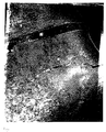
- Im folgenden wird ein Ausführungsbeispiel des erfindungsgemäßen Verfahrens anhand einer elektronenmikroskopischen Aufnahme eines SrTiO₃-YBa₂Cu₃O₇-Schichtsystems beschrieben.
- Gezeigt wird ein unkontrolliert gewachsener Bereich einer YBa₂Cu₃O₇-Schicht 1, eine anschließend wenige nm dick aufgetragene SrTiO₃-Schicht 2, eine weiter unkontrolliert gewachsene YBa₂Cu₃O₇-Schicht 3 eine dann 20 nm bis 30 nm dick aufgetragene SrTiO₃-Schicht 5 und ein dadurch hervorgerufenes gleichmäßiges c-Achsen-orientiertes Wachstum der folgenden YBa₂Cu₃O₇-Schicht 7.
- c-Achsen-orientierte Bereiche erscheinen in der Darstellung quer-, a-Achsen-orientierte Bereiche längsgestreift. Die 20 nm bis 30 nm dicke SrTiO₃-Schicht überdeckt die Stufe 6 und verursachte so ein c-Achsen-orientiertes Wachstum der YBa₂Cu₃O₇-Schicht 7. Es ist deutlich zu erkennen, daß dagegen die dünn aufgetragene SrTiO₃-Schicht 2 nicht in der Lage ist, die Stufe 4 zu überdecken und von dieser Stufe dann ein weiteres a-Achsen-orientierte Wachstum ausgeht.
- Das Auftragen von YBa₂Cu₃O₇ erfolgte durch Hochdruck-dc Sputtern unter folgenden Bedingungen
- einzelnes stöchiometrisches Target mit 35 mm φ
- (100)-orientierter SrTiO₃-Kristall als Substrat
- 13 mm Abstand zwischen Target und Substrat
- Sauerstoff als Sputtergas bei einem Druck von 3,6 mbar
- Ofentemperatur von 880°C
- Oberflächentemperatur des Substrats bei 750°C
- Stromstärke während des Sputterns von 200 mA
- Sauerstoffnachbehandlung bei 550°C.
- SrTiO₃-Schichten wurden durch Hochfrequenz-Sputtern bei einer Sinusspannung vom 1000 V, einer Wechselstromfrequenz von 7 MHz und unter ansonsten gleichen Bedingungen aufgebracht.
Claims (4)
- Verfahren zur Herstellung eines Schichtsystems mit Substrat und darauf aufgewachsener c-Achsen kristallorientierter YBa₂Cu₃O₇-Schicht,
dadurch gekennzeichnet,
daß das Wachstum der YBa₂Cu₃O₇-Schicht bei Auftreten unerwünschter a-Achsen-orientierter Bereiche und dabei zwischen a-Achsen-und c-Achsen-orientierten Bereichen auf der YBa₂Cu₃O₇-Oberfläche entstandener Stufen unterbrochen, eine SrTiO₃-Schicht solange aufgetragen wird, bis die Stufen überdeckt sind und anschließend das Wachstum der YBa₂Cu₃O₇-Schicht fortgesetzt wird. - Verfahren nach Anspruch 1,
dadurch gekennzeichnet,
daß eine SrTiO₃-Schicht, die die Stufen auf der YBa₂Cu₃O₇-Schicht überdeckt, in einer Schichtdicke von 20 nm bis 30 nm aufgetragen wird. - Schichtsystem bestehend aus SrTiO₃ und c-Achsenkristallorientiertem YBa₂Cu₃O₇,
dadurch gekennzeichnet,
daß das Schichtsystem aus mehreren sich abwechselnden SrTiO₃- und YBa₂Cu₃O₇-Schichten besteht und die SrTiO₃-Schichten, die zwischen zwei YBa₂Cu₃O₇-Schichten liegen, 20 nm bis 30 nm dick sind. - Schichtsystem nach Anspruch 3,
dadurch gekennzeichnet,
daß YBa₂Cu₃O₇-Schichten 300 nm bis 500 nm dick sind.
Applications Claiming Priority (2)
| Application Number | Priority Date | Filing Date | Title |
|---|---|---|---|
| DE4136126A DE4136126C2 (de) | 1991-11-02 | 1991-11-02 | Verfahren zur Herstellung eines SrTiO¶3¶-YBa¶2¶Cu¶3¶O¶7¶-Schichtsystems und Schichtsystem aus SrTiO¶3¶ und YBa¶2¶Cu¶3¶O¶7¶ |
| DE4136126 | 1991-11-02 |
Publications (2)
| Publication Number | Publication Date |
|---|---|
| EP0541011A1 EP0541011A1 (de) | 1993-05-12 |
| EP0541011B1 true EP0541011B1 (de) | 1996-04-17 |
Family
ID=6443952
Family Applications (1)
| Application Number | Title | Priority Date | Filing Date |
|---|---|---|---|
| EP92118576A Expired - Lifetime EP0541011B1 (de) | 1991-11-02 | 1992-10-30 | Verfahren zur Herstellung eines SrTiO3-YBa2Cu3O7-Schichtsystems und Schichtsystem aus SrTiO3 und YBa2Cu3O7 |
Country Status (4)
| Country | Link |
|---|---|
| US (1) | US5430014A (de) |
| EP (1) | EP0541011B1 (de) |
| JP (1) | JPH05214513A (de) |
| DE (2) | DE4136126C2 (de) |
Families Citing this family (7)
| Publication number | Priority date | Publication date | Assignee | Title |
|---|---|---|---|---|
| DE4136126C2 (de) * | 1991-11-02 | 1994-06-30 | Forschungszentrum Juelich Gmbh | Verfahren zur Herstellung eines SrTiO¶3¶-YBa¶2¶Cu¶3¶O¶7¶-Schichtsystems und Schichtsystem aus SrTiO¶3¶ und YBa¶2¶Cu¶3¶O¶7¶ |
| US5892243A (en) * | 1996-12-06 | 1999-04-06 | Trw Inc. | High-temperature SSNS and SNS Josephson junction and method of making junction |
| US6383989B2 (en) * | 2000-06-21 | 2002-05-07 | The Regents Of The University Of California | Architecture for high critical current superconducting tapes |
| US6635368B1 (en) * | 2001-12-20 | 2003-10-21 | The United States Of America As Represented By The Secretary Of The Navy | HTS film-based electronic device characterized by low ELF and white noise |
| US6830776B1 (en) | 2002-02-08 | 2004-12-14 | The United States Of America As Represented By The Secretary Of The Air Force | Method of manufacturing a high temperature superconductor |
| WO2012135683A1 (en) * | 2011-03-30 | 2012-10-04 | Ambature Llc | Electrical, mechanical, computing, and/or other devices formed of extremely low resistance materials |
| US9355362B2 (en) * | 2011-11-11 | 2016-05-31 | Northrop Grumman Systems Corporation | Quantum bits and method of forming the same |
Family Cites Families (3)
| Publication number | Priority date | Publication date | Assignee | Title |
|---|---|---|---|---|
| JPH03270280A (ja) * | 1990-03-09 | 1991-12-02 | Univ California | 超伝導交差路を有する微小電子回路素子及び製造方法 |
| US5215960A (en) * | 1990-07-02 | 1993-06-01 | Sumitomo Electric Industries, Ltd. | Method for manufacturing oxide superconducting devices |
| DE4136126C2 (de) * | 1991-11-02 | 1994-06-30 | Forschungszentrum Juelich Gmbh | Verfahren zur Herstellung eines SrTiO¶3¶-YBa¶2¶Cu¶3¶O¶7¶-Schichtsystems und Schichtsystem aus SrTiO¶3¶ und YBa¶2¶Cu¶3¶O¶7¶ |
-
1991
- 1991-11-02 DE DE4136126A patent/DE4136126C2/de not_active Expired - Fee Related
-
1992
- 1992-10-30 DE DE59206031T patent/DE59206031D1/de not_active Expired - Lifetime
- 1992-10-30 US US08/061,715 patent/US5430014A/en not_active Expired - Fee Related
- 1992-10-30 JP JP4293387A patent/JPH05214513A/ja active Pending
- 1992-10-30 EP EP92118576A patent/EP0541011B1/de not_active Expired - Lifetime
Also Published As
| Publication number | Publication date |
|---|---|
| DE4136126C2 (de) | 1994-06-30 |
| US5430014A (en) | 1995-07-04 |
| EP0541011A1 (de) | 1993-05-12 |
| DE59206031D1 (de) | 1996-05-23 |
| JPH05214513A (ja) | 1993-08-24 |
| DE4136126A1 (de) | 1993-05-06 |
Similar Documents
| Publication | Publication Date | Title |
|---|---|---|
| DE69028471T2 (de) | Draht aus supraleiteroxyd, verfahren zur herstellung und so erzeugter gegenstand | |
| DE69218895T2 (de) | Supraleitende Mehrschichtenverschaltung aus supraleitendem oxidischen Material und Verfahren zu ihrer Herstellung | |
| DE69115209T2 (de) | Verfahren zur Herstellung eines Supraleitungsbauelements mit reduzierter Dicke der supraleitenden Oxidschicht und dadurch hergestelltes Supraleitungsbauelement. | |
| DE69115957T2 (de) | Verfahren zum Herstellen hochtemperatursupraleitender Dünnschichten | |
| WO1999022412A1 (de) | Supraleiteraufbau mit glassubstrat und darauf abgeschiedenem hochtemperatursupraleiter sowie verfahren zur herstellung des aufbaus | |
| DE69112520T2 (de) | Supraleitende Dünnschicht-Oxydverbindung und Verfahren zu deren Herstellung. | |
| DE4136126C2 (de) | Verfahren zur Herstellung eines SrTiO¶3¶-YBa¶2¶Cu¶3¶O¶7¶-Schichtsystems und Schichtsystem aus SrTiO¶3¶ und YBa¶2¶Cu¶3¶O¶7¶ | |
| DE69212670T2 (de) | Supraleitende oxydische Dünnschicht mit lokal unterschiedlichen Kristallorientierungen und ein Verfahren zu deren Herstellung | |
| DE3854626T2 (de) | Verfahren zur Herstellung von Komponenten aus supraleitenden oxidkeramischen Materialien. | |
| DE69300940T2 (de) | Josephson-Übergangseinrichtung aus oxidischem Supraleiter und Verfahren zu ihrer Herstellung. | |
| DE69017112T2 (de) | Supraleitende Dünnschicht aus Oxid und Verfahren zu deren Herstellung. | |
| DE69218735T2 (de) | Verfahren zum Herstellen eines künstlichen Josephson-Korngrenzen-Übergangselementes | |
| DE68917779T2 (de) | Josephson-Einrichtung und Verfahren zu ihrer Herstellung. | |
| DE69117378T2 (de) | Supraleitende Einrichtung mit geschichteter Struktur, zusammengesetzt aus oxidischem Supraleiter und Isolatordünnschicht und deren Herstellungsmethode | |
| DE69128753T2 (de) | Verfahren zur Herstellung einer supraleitenden Einrichtung mit reduzierter Dicke der supraleitenden Schicht und dadurch hergestellte supraleitende Einrichtung | |
| DE69218388T2 (de) | Supraleitendes Bauelement mit extrem dünnem Kanal aus supraleitendem Oxyd und sein Herstellungsverfahren | |
| DE3886429T2 (de) | Verfahren zum Herstellen einer supraleitenden Dünnschicht. | |
| DE69220387T2 (de) | Verfahren zur Herstellung eines Tunnelüberganges von der Art einer Josephson-Einrichtung aufgebaut aus supraleitendem oxydischem Verbundmaterial | |
| DE69309830T2 (de) | Supraleitende dünne Schicht und ihr Herstellungsverfahren | |
| DE69210523T2 (de) | Verfahren zur Herstellung von supraleitenden Schichten aus supraleitendem Oxyd in denen nicht-supraleitende Gebiete vorkommen und Verfahren zur Herstellung eines Bauelements welches solche Schichten enthält | |
| DE69010445T2 (de) | Supraleitende Einrichtung. | |
| DE69127719T2 (de) | Verfahren zur Herstellung eines supraleitenden Überganges aus oxydischem Supraleiter | |
| DE69112282T2 (de) | Verfahren zur Herstellung Hochtemperatur supraleitender Dünnschichten. | |
| DE69131611T2 (de) | Verfahren zur Herstellung dünner Schichten aus Oxyd-Supraleiter | |
| EP0330899B1 (de) | Verfahren zur Herstellung einer Schicht aus einem metalloxidischen Supraleitermaterial mit hoher Sprungtemperatur und Vorrichtung zur Durchführung des Verfahrens |
Legal Events
| Date | Code | Title | Description |
|---|---|---|---|
| PUAI | Public reference made under article 153(3) epc to a published international application that has entered the european phase |
Free format text: ORIGINAL CODE: 0009012 |
|
| AK | Designated contracting states |
Kind code of ref document: A1 Designated state(s): DE FR NL |
|
| 17P | Request for examination filed |
Effective date: 19931011 |
|
| 17Q | First examination report despatched |
Effective date: 19950127 |
|
| GRAH | Despatch of communication of intention to grant a patent |
Free format text: ORIGINAL CODE: EPIDOS IGRA |
|
| GRAA | (expected) grant |
Free format text: ORIGINAL CODE: 0009210 |
|
| AK | Designated contracting states |
Kind code of ref document: B1 Designated state(s): DE FR NL |
|
| REF | Corresponds to: |
Ref document number: 59206031 Country of ref document: DE Date of ref document: 19960523 |
|
| ET | Fr: translation filed | ||
| PLBE | No opposition filed within time limit |
Free format text: ORIGINAL CODE: 0009261 |
|
| STAA | Information on the status of an ep patent application or granted ep patent |
Free format text: STATUS: NO OPPOSITION FILED WITHIN TIME LIMIT |
|
| 26N | No opposition filed | ||
| PGFP | Annual fee paid to national office [announced via postgrant information from national office to epo] |
Ref country code: NL Payment date: 20111025 Year of fee payment: 20 Ref country code: FR Payment date: 20111103 Year of fee payment: 20 |
|
| PGFP | Annual fee paid to national office [announced via postgrant information from national office to epo] |
Ref country code: DE Payment date: 20110907 Year of fee payment: 20 |
|
| REG | Reference to a national code |
Ref country code: DE Ref legal event code: R071 Ref document number: 59206031 Country of ref document: DE |
|
| REG | Reference to a national code |
Ref country code: DE Ref legal event code: R071 Ref document number: 59206031 Country of ref document: DE |
|
| REG | Reference to a national code |
Ref country code: NL Ref legal event code: V4 Effective date: 20121030 |