EP0540450A1 - Fehlerkodekorrekturfunktion mit partiellem Schreibzugriff oder Lese-/Änder-/Schreibzugriff und Schnittstellenschema mit Paritätsvorgriff - Google Patents
Fehlerkodekorrekturfunktion mit partiellem Schreibzugriff oder Lese-/Änder-/Schreibzugriff und Schnittstellenschema mit Paritätsvorgriff Download PDFInfo
- Publication number
- EP0540450A1 EP0540450A1 EP92480152A EP92480152A EP0540450A1 EP 0540450 A1 EP0540450 A1 EP 0540450A1 EP 92480152 A EP92480152 A EP 92480152A EP 92480152 A EP92480152 A EP 92480152A EP 0540450 A1 EP0540450 A1 EP 0540450A1
- Authority
- EP
- European Patent Office
- Prior art keywords
- parity
- bits
- memory
- data
- bus
- Prior art date
- Legal status (The legal status is an assumption and is not a legal conclusion. Google has not performed a legal analysis and makes no representation as to the accuracy of the status listed.)
- Granted
Links
Images


Classifications
-
- G—PHYSICS
- G06—COMPUTING; CALCULATING OR COUNTING
- G06F—ELECTRIC DIGITAL DATA PROCESSING
- G06F11/00—Error detection; Error correction; Monitoring
- G06F11/07—Responding to the occurrence of a fault, e.g. fault tolerance
- G06F11/08—Error detection or correction by redundancy in data representation, e.g. by using checking codes
- G06F11/10—Adding special bits or symbols to the coded information, e.g. parity check, casting out 9's or 11's
- G06F11/1008—Adding special bits or symbols to the coded information, e.g. parity check, casting out 9's or 11's in individual solid state devices
- G06F11/1048—Adding special bits or symbols to the coded information, e.g. parity check, casting out 9's or 11's in individual solid state devices using arrangements adapted for a specific error detection or correction feature
- G06F11/1056—Updating check bits on partial write, i.e. read/modify/write
Definitions
- the present invention generally relates to error detecting and/or correcting schemes for digital computers and, more particularly, to an error correcting code (ECC) function especially useful for memory systems in personal computers (PCs) and to a parity interface scheme providing a translation capability between the ECC and parity protocols.
- ECC error correcting code
- ECC error correcting code
- ECC error correcting code
- the check bits that are stored with the data are generated based on the entire thirty-two bits. This makes it necessary to regenerate all of the check bits if even one data bit has changed.
- the entire 4-byte double word must first be read, checked and corrected, the new eight bits substituted, and then all four bytes must be rewritten to memory with the appropriate new check bits. The same is true if two or three bytes of data need to be written to memory. This is called a partial write or a read/modify/write operation.
- U.S. Patent No. 4,884,271 to Concha et al. describes a method for handling the read/modify/write problem which uses a correct-on-error scheme where check bits are generated on uncorrected data and then regenerated if the data is found to be in error.
- This requires a "long” and a “short” read/modify/write cycle, as well as two types of read cycles, to handle data with or without errors, respectively.
- This approach suffers from being relatively complex in operation.
- the correct-on-error scheme allows data processing to begin while the ECC logic determines if an error is present. This has a disadvantage in that the processor must back up and discard the corrupt data when an error occurs.
- U.S. Patent No. 4,852,100 to Christensen et al. describes an error correction and detection method which, like the Concha et al. patent, also incorporates a correct-on-error scheme with multiple ECC sub-blocks.
- Christensen et al. like Kocol et al., do not address the problems of interfacing memory with a variety of other components that may communicate in words composed of different numbers of bytes.
- Christensen et al. use a single ECC unit to handle data of varying numbers of bytes.
- Column 5 of the Christensen et al. patent describes the dedication of an ECC unit to each sub-block of data for various reasons. While the Christensen et al. approach could be employed to address the problem of storing words of varying numbers of bytes, it is generally not feasible due to the excessive overhead on the number of bit paths and consequently cost and space.
- ECC Error Correction Code
- an improved ECC system which allows data of varying byte lengths to be written to memory without the overhead of prior art solutions and with minimal use of the system bus.
- the partial write function is accomplished through the use of internal multiplexing so that the handling of unmodified data is minimized. This is done by overlaying the selected bytes of data read from memory with the new bytes directly within the ECC logic.
- an appropriate ECC code is chosen to facilitate parity generation and checking. This is done by selecting a code that contains groupings of data bits corresponding to the desired parity scheme.
- the ECC XOR trees are modified to allow parity checking and error correction decode simultaneously, thereby eliminating the need for two sets of XOR trees in the interface.
- a parity protocol is implemented on the system bus and an ECC protocol is implemented on the memory bus.
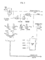
- a 32-bit microprocessor 10 such as an Intel 80386 or 80486 or a Motorola 68030 or 68040 microprocessor, is connected to a 32-bit system bus 12.
- An 8-bit component 14 such as for example, a floppy disk controller board, is connected to the system bus 12, and a 16-bit component 16, such as for example a video display adapter, is also connected to the system bus 12.
- Other components (not shown), either 8-bit or 16-bit, such as a combination facsimile/modem adapter or hard drive controller, may also be connected to the system bus 12.
- the system bus 12 is connected to a dedicated 32-bit memory bus 18 by which data is read from or written to a random access memory (RAM) 20.
- RAM random access memory
- the connection between the two buses is via a parity interface 22 and 32-bit ECC logic 24.
- the invention combines the functions of the parity interface 22 and the ECC logic 24 in a single unit, eliminating redundant logic and overhead thereby conserving valuable silicon real estate and improving speed of operation.
- the ECC protocol for the memory bus 18 is thirty-two data bits and seven check bits, while the parity protocol for the system bus 12 is thirty-two data bits and four parity bits.
- each component attached to the system bus 12, including the parity interface 22, must generate parity when sending to the system bus 12 and must check parity when receiving data from the system bus 12.
- XOR Exclusive OR
- Figure 2 For a 32-bit bus, four three level Exclusive OR (XOR) trees are typically used to generate and check the four parity bits, one for each byte of data.
- XOR Exclusive OR
- Figure 2 One such tree is shown in Figure 2 and comprises seven XOR gates, plus some additional control logic (not shown).
- Such parity circuits are well known to those skilled in the art and, therefore, need not be described in detail. It is only noted here that the overhead for parity on a group of data bits is the silicon area required for the additional logic plus the delay in generating and checking the parity bits by the XOR gate trees.
- FIG 3 shows an implementation of an ECC code consisting of thirty-two data bits and seven check bits. This code is capable of correcting all single bit errors and detecting all double bit errors.
- seven four level XOR trees 26 are used to generate seven check bits. Each XOR tree has inputs from an overlapping subset of the thirty-two data bits, providing a unique coverage pattern for each bit.
- the seven received check bits are compared to the outputs of the seven XOR trees 26 in seven XOR gates 27, only one of which is shown for the sake of clarity, to determine if an error is present.
- the outputs of the seven XOR gates 27 are input to a seven input OR gate 33 which provides an output to the system that an error has been detected regardless of whether or not it can be corrected. Thus, an all zero syndrome indicates no error.
- the outputs of AND gates 300 to 3038 are input to a 39-bit (thirty-two data and seven check bits) NOR gate 34.
- a logic "1" output from the NOR gate 34 reflects the fact that no matching correctable error decode pattern has been detected (i.e., none of the AND gates 30 i , 0 ⁇ i ⁇ 38, output a logic "1").
- a logic "1" output from NOR gate 34 enables AND gate 36. Then, if an error is detected, as indicated by a logic "1" output of the OR gate 33, AND gate 36 out-puts a logic "1" to report an"uncorrectable error to the system.
- the check bits are simply generated by the seven XOR trees 26 and combined with the data.
- Figure 4 shows the classical method of interfacing between a system bus using parity and a memory bus that has implemented ECC.
- the parity logic 40 comprises four XOR trees, of the type shown in Figure 2, plus associated logic.
- the ECC logic 42 comprises seven XOR trees, and associated logic of the type shown in Figure 3.
- bus "2" i.e., memory bus 18
- bus "1" i.e., system bus 12
- FIG. 1 shows an example of a prior art method of implementing a partial write function.
- the interface between the system bus 12 and the memory bus 18 comprises four 8-bit bidirectional (BIDI) buffers 44, 46, 48, and 50.
- BIDI bidirectional bidirectional
- a 32-bit ECC module 24 is connected to the memory bus 18, as previously described.
- the ECC module 24, for example, reads four bytes from memory, correcting and/or indicating any errors, and sends only the data that is not being changed back onto the dedicated memory bus 18.
- the four 8-bit buffers 44, 46, 48, and 50 are then either placed into active mode or held in tri-state mode so that the new byte of data together with the three unchanged bytes appear at the input/output (I/O) ports of the ECC module 24.
- the ECC module then reads the data in, generates new check bits and writes the combination to memory 20. The same can be done for two or three bytes of data being changed, either from the microprocessor 10 or, for example, by a 16-bit component connected to the system bus 12.
- FIG. 6 shows in detail the preferred embodiment of the improved ECC logic according to a first aspect of the present invention.
- the thirty-two data bit lines of bidirectional memory bus 18 are connected to both a receiver block 52 and a driver block 54.
- the thirty-two data bit lines from receiver block 52 are, in turn, connected to a set of XOR trees 58 and decode and correcting logic 60.
- the XOR trees 58 comprise seven trees, four of which generate both a parity bit and a check bit while the remaining three generate only check bits.
- the seven check bit lines of the memory bus 18 are likewise connected to both a receiver block 62 and driver block 64.
- the output of the receiver block 62 is supplied to the XOR trees 58, the output of which is supplied to the decode and correcting logic 60.
- the decode and correcting logic 60 has five outputs.
- One output comprises thirty-two data bit lines to a tri-state receiver block 66.
- a second output comprises seven check bit lines to the driver block 64.
- there are two error outputs one to a single error driver 70 and the other to a multiple error driver 72.
- There is also a parity error driver 74 which outputs a parity error flag to the system bus 12 in response to an output from a parity generator and checking logic 75, described in more detail hereinafter with reference to Figure 10.
- the logic 75 receives four parity correction outputs from the decode and correcting logic 60 and four parity outputs from the XOR trees 58 and communicates with the four parity lines on the system bus 12 via receiver block 76
- the thirty-two data bit lines of bidirectional system bus 12 are connected to both a tri-state receiver block 78 and a driver block 79.
- the thirty-two data bit lines from tri-state receiver block 78 are, in turn, connected to each of the XOR trees 58 and the driver block 54.
- the partial write function is accomplished through internal multiplexing by overlaying the selected bytes of data read from memory with the new bytes as follows:
- each receiver block 52, 62, 76, and 78 also contain transparent latches which can be used to free up the external system and memory buses in a very short period of time.
- the first aspect of the present invention provides savings in both external components and delay without any impact to the normal ECC write and read performance.
- the second aspect of the present invention relates to the interface between the system bus which implements a parity check protocol and the memory bus which implements an ECC protocol.
- a parity check protocol For a 32-bit data bus, four three-level XOR trees are typically used to generate and check the four parity bits, one for each byte of data.
- the prior art approach shown in Figure 4, is to use an additional seven four-level XOR trees.
- the overhead for parity and ECC on a group of data bits is, therefore, the silicon area required for the additional logic plus the delay in generating and checking the parity bits by the XOR trees.
- the second aspect of the invention contemplates the elimination of the inherent redundancy of two sets of XOR trees, one for parity generation and check and one for check bit generation and check.
- the first level comprises eight XOR gates 821 to 828.
- the inputs to these XOR gates are denoted by the letters A to P, inclusive.
- the second level comprises four XOR gates 841 to 844, with each pair of XOR gates 821 to 828 providing inputs to XOR gates 841 to 844.
- the third level comprises two XOR gates 861 and 862, again with each pair of XOR gates 841 to 844 providing inputs to XOR gates 861 and 862.
- the output of XOR gate 861 is the parity bit IBP i , 0 ⁇ i ⁇ 3, for one of the four bytes of data.
- the fourth level of the XOR tree comprises the single XOR gate 88 which receives as its inputs the outputs of XOR gates 861 and 862.
- the output of XOR gate 88 is the ECC check bit T n , 0 ⁇ n ⁇ 6, for the data inputs A through P.
- an appropriate ECC code is chosen so that the job of parity generation and checking can be made easier. This is done by selecting a code that contains groupings of data bits in its XOR trees corresponding to the desired parity scheme.
- Table 1 in Figure 8 illustrates an example of such a code developed by C. L. Chen and M. Y. Hsiao of International Business Machines Corp.
- Each row of Table 1 represents an XOR tree.
- the "Xs” indicate data bits that are inputs to the corresponding tree.
- XOR tree “1” has, among its inputs, data bits 0 through 7. Once corrected, these eight bits are used to generate parity bit 0 for the system bus.
- Tree “2” has inputs from data bits 8 through 15, which correspond to parity bit 1.
- trees "4" and "5" contain the bits necessary to produce parity bits 2 and 3, respectively. Given a code such as this, several of the XOR trees may be constructed so that an intermediate node in each of them will represent a parity bit over a given byte of data, as shown in Figure 7.
- Figure 9 is a modification of the ECC code implementation shown in Figure 3, substituting the XOR trees 58 of Figure 6 which include four XOR trees as shown in Figure 7. Note that the 39-way NOR gate 34 has been replaced with five NOR gates 90, 92, 94, 96, and 98. Each of the first four NOR gates has inputs from eight AND gates that perform the decode function for a given byte.
- the outputs of the four XOR trees shown in Figure 7, denoted as IBP(i), 0 ⁇ i ⁇ 3, are also the parity bits; however, these parity bits are not necessarily correct. If any one of the data bits was in error, the corresponding parity bit will be generated based on the uncorrected data and be in error as well. Recall that the data is not yet corrected as it enters the ECC XOR trees. Therefore, when the single bit error in the data is later corrected, the parity will no longer reflect the data properly.
- each of the NOR gate outputs is that each indicates if a correctable error has occurred within that byte of data. This signal may then be used to determine which parity bit must be flipped in order to properly reflect the corrected data sent out onto the system bus 12.
- Figure 10 illustrates the logic necessary to complete the parity generation.
- the BPE i 0 ⁇ i ⁇ 3, signal outputs from the NOR gates 90, 92, 94, and 96, is compared by a respective XOR gate 100 (only one of which is shown for clarity) with the internal parity node (see Figure 7) from an ECC XOR tree (IBP i , 0 ⁇ i ⁇ 3) to produce the correct parity bit output for transfers from memory bus 18 to system bus 12.
Landscapes
- Engineering & Computer Science (AREA)
- Theoretical Computer Science (AREA)
- Quality & Reliability (AREA)
- Physics & Mathematics (AREA)
- General Engineering & Computer Science (AREA)
- General Physics & Mathematics (AREA)
- Detection And Correction Of Errors (AREA)
- Techniques For Improving Reliability Of Storages (AREA)
- Debugging And Monitoring (AREA)
- Bus Control (AREA)
Applications Claiming Priority (2)
| Application Number | Priority Date | Filing Date | Title |
|---|---|---|---|
| US785558 | 1991-10-31 | ||
| US07/785,558 US5313475A (en) | 1991-10-31 | 1991-10-31 | ECC function with self-contained high performance partial write or read/modify/write and parity look-ahead interface scheme |
Publications (2)
| Publication Number | Publication Date |
|---|---|
| EP0540450A1 true EP0540450A1 (de) | 1993-05-05 |
| EP0540450B1 EP0540450B1 (de) | 1997-06-18 |
Family
ID=25135884
Family Applications (1)
| Application Number | Title | Priority Date | Filing Date |
|---|---|---|---|
| EP92480152A Expired - Lifetime EP0540450B1 (de) | 1991-10-31 | 1992-10-09 | Fehlerkodekorrekturfunktion mit partiellem Schreibzugriff oder Lese-/Änder-/Schreibzugriff und Schnittstellenschema mit Paritätsvorgriff |
Country Status (4)
| Country | Link |
|---|---|
| US (1) | US5313475A (de) |
| EP (1) | EP0540450B1 (de) |
| JP (1) | JP2512666B2 (de) |
| DE (1) | DE69220452D1 (de) |
Cited By (4)
| Publication number | Priority date | Publication date | Assignee | Title |
|---|---|---|---|---|
| EP0668561A2 (de) * | 1994-02-22 | 1995-08-23 | Siemens Aktiengesellschaft | Flexible Fehlerkorrekturcode/Paritätsbit-Architektur |
| EP0730228A1 (de) * | 1995-03-03 | 1996-09-04 | Hal Computer Systems, Inc. | ECC-geschützte Speicherorganisation mit Lese-Änderungs-Schreib-Pipelinezugriff |
| EP2326014A3 (de) * | 2009-11-18 | 2013-01-02 | Fujitsu Limited | Schaltung zur Erzeugung von Fehlererkennungs-/-korrekturcodes und Steuerverfahren dafür |
| US8993219B2 (en) | 2011-06-21 | 2015-03-31 | Basf Se | Printing diffraction gratings on paper and board |
Families Citing this family (65)
| Publication number | Priority date | Publication date | Assignee | Title |
|---|---|---|---|---|
| US5455939A (en) * | 1992-06-17 | 1995-10-03 | Intel Corporation | Method and apparatus for error detection and correction of data transferred between a CPU and system memory |
| US5430742A (en) * | 1992-10-14 | 1995-07-04 | Ast Research, Inc. | Memory controller with ECC and data streaming control |
| US5790776A (en) * | 1992-12-17 | 1998-08-04 | Tandem Computers Incorporated | Apparatus for detecting divergence between a pair of duplexed, synchronized processor elements |
| US5481552A (en) * | 1993-12-30 | 1996-01-02 | International Business Machines Corporation | Method and structure for providing error correction code for 8-byte data words on SIMM cards |
| US5594862A (en) * | 1994-07-20 | 1997-01-14 | Emc Corporation | XOR controller for a storage subsystem |
| US5561765A (en) * | 1994-07-27 | 1996-10-01 | Siemens Rolm Communications, Inc. | Algorithm for testing a memory |
| US5771247A (en) * | 1994-10-03 | 1998-06-23 | International Business Machines Corporation | Low latency error reporting for high performance bus |
| US5774481A (en) * | 1995-03-31 | 1998-06-30 | International Business Machines Corporation | Reduced gate error detection and correction circuit |
| US5922080A (en) * | 1996-05-29 | 1999-07-13 | Compaq Computer Corporation, Inc. | Method and apparatus for performing error detection and correction with memory devices |
| US5961660A (en) * | 1997-03-03 | 1999-10-05 | International Business Machines Corporation | Method and apparatus for optimizing ECC memory performance |
| US6363511B1 (en) | 1998-03-31 | 2002-03-26 | Stmicroelectronics N.V. | Device and method for decoding data streams from storage media |
| US6260169B1 (en) * | 1998-03-31 | 2001-07-10 | Stmicroelectronics N.V. | Device and method for real time correction of row data from DVD media |
| US6728920B1 (en) | 1999-05-24 | 2004-04-27 | Adaptive Broadband Corporation | Method for correcting errors in transfer of information |
| TW519663B (en) * | 2001-05-15 | 2003-02-01 | Via Tech Inc | Memory control device and method |
| US7340659B2 (en) * | 2002-05-15 | 2008-03-04 | Infineon Technologies, A.G. | Method of testing multiple modules on an integrated circuit |
| US7305519B1 (en) | 2004-03-29 | 2007-12-04 | Cisco Technology, Inc. | Error protection for associative memory entries and lookup operations performed thereon |
| US7099221B2 (en) | 2004-05-06 | 2006-08-29 | Micron Technology, Inc. | Memory controller method and system compensating for memory cell data losses |
| US20060010339A1 (en) * | 2004-06-24 | 2006-01-12 | Klein Dean A | Memory system and method having selective ECC during low power refresh |
| US7340668B2 (en) * | 2004-06-25 | 2008-03-04 | Micron Technology, Inc. | Low power cost-effective ECC memory system and method |
| US7290083B2 (en) * | 2004-06-29 | 2007-10-30 | Cisco Technology, Inc. | Error protection for lookup operations in content-addressable memory entries |
| US7116602B2 (en) | 2004-07-15 | 2006-10-03 | Micron Technology, Inc. | Method and system for controlling refresh to avoid memory cell data losses |
| US6965537B1 (en) * | 2004-08-31 | 2005-11-15 | Micron Technology, Inc. | Memory system and method using ECC to achieve low power refresh |
| WO2006039556A2 (en) * | 2004-10-02 | 2006-04-13 | Wms Gaming Inc. | Gaming device with error correcting memory |
| US7350131B2 (en) * | 2005-01-22 | 2008-03-25 | Cisco Technology, Inc. | Error protecting groups of data words |
| US7689889B2 (en) * | 2006-08-24 | 2010-03-30 | Cisco Technology, Inc. | Content addressable memory entry coding for error detection and correction |
| US7894289B2 (en) * | 2006-10-11 | 2011-02-22 | Micron Technology, Inc. | Memory system and method using partial ECC to achieve low power refresh and fast access to data |
| US7900120B2 (en) | 2006-10-18 | 2011-03-01 | Micron Technology, Inc. | Memory system and method using ECC with flag bit to identify modified data |
| US8443134B2 (en) * | 2006-12-06 | 2013-05-14 | Fusion-Io, Inc. | Apparatus, system, and method for graceful cache device degradation |
| US8489817B2 (en) | 2007-12-06 | 2013-07-16 | Fusion-Io, Inc. | Apparatus, system, and method for caching data |
| US8706968B2 (en) * | 2007-12-06 | 2014-04-22 | Fusion-Io, Inc. | Apparatus, system, and method for redundant write caching |
| US9104599B2 (en) | 2007-12-06 | 2015-08-11 | Intelligent Intellectual Property Holdings 2 Llc | Apparatus, system, and method for destaging cached data |
| US9495241B2 (en) | 2006-12-06 | 2016-11-15 | Longitude Enterprise Flash S.A.R.L. | Systems and methods for adaptive data storage |
| US9116823B2 (en) | 2006-12-06 | 2015-08-25 | Intelligent Intellectual Property Holdings 2 Llc | Systems and methods for adaptive error-correction coding |
| JP2010512584A (ja) * | 2006-12-06 | 2010-04-22 | フュージョン マルチシステムズ,インク.(ディービイエイ フュージョン−アイオー) | 空データトークン指令を有する要求デバイスからのデータを管理する装置、システムおよび方法 |
| WO2008155850A1 (ja) * | 2007-06-20 | 2008-12-24 | Fujitsu Limited | キャッシュ制御装置、キャッシュ制御方法およびキャッシュ制御プログラム |
| US8316277B2 (en) * | 2007-12-06 | 2012-11-20 | Fusion-Io, Inc. | Apparatus, system, and method for ensuring data validity in a data storage process |
| US9519540B2 (en) | 2007-12-06 | 2016-12-13 | Sandisk Technologies Llc | Apparatus, system, and method for destaging cached data |
| US7836226B2 (en) | 2007-12-06 | 2010-11-16 | Fusion-Io, Inc. | Apparatus, system, and method for coordinating storage requests in a multi-processor/multi-thread environment |
| US7523379B1 (en) | 2008-03-31 | 2009-04-21 | International Business Machines Corporation | Method for time-delayed data protection |
| JP2010204828A (ja) * | 2009-03-02 | 2010-09-16 | Renesas Electronics Corp | データ保護回路及び方法、並びにデータ処理装置 |
| CN102696010B (zh) | 2009-09-08 | 2016-03-23 | 才智知识产权控股公司(2) | 用于将数据高速缓存在固态存储设备上的装置、系统和方法 |
| US9166624B2 (en) | 2010-05-11 | 2015-10-20 | Osaka University | Error-correcting code processing method and device |
| US9092337B2 (en) | 2011-01-31 | 2015-07-28 | Intelligent Intellectual Property Holdings 2 Llc | Apparatus, system, and method for managing eviction of data |
| US9003104B2 (en) | 2011-02-15 | 2015-04-07 | Intelligent Intellectual Property Holdings 2 Llc | Systems and methods for a file-level cache |
| US8874823B2 (en) | 2011-02-15 | 2014-10-28 | Intellectual Property Holdings 2 Llc | Systems and methods for managing data input/output operations |
| US9201677B2 (en) | 2011-05-23 | 2015-12-01 | Intelligent Intellectual Property Holdings 2 Llc | Managing data input/output operations |
| WO2012116369A2 (en) | 2011-02-25 | 2012-08-30 | Fusion-Io, Inc. | Apparatus, system, and method for managing contents of a cache |
| US9003260B2 (en) * | 2011-06-29 | 2015-04-07 | Texas Instruments Incorporated | Partial-writes to ECC (error check code) enabled memories |
| US8751905B2 (en) | 2011-09-16 | 2014-06-10 | Avalanche Technology, Inc. | Memory with on-chip error correction |
| US9251882B2 (en) | 2011-09-16 | 2016-02-02 | Avalanche Technology, Inc. | Magnetic random access memory with dynamic random access memory (DRAM)-like interface |
| US9658780B2 (en) | 2011-09-16 | 2017-05-23 | Avalanche Technology, Inc. | Magnetic random access memory with dynamic random access memory (DRAM)-like interface |
| US9054840B2 (en) | 2011-12-15 | 2015-06-09 | Lenovo Enterprise Solutions (Singapore) Pte. Ltd. | Error detection and correction of a data transmission |
| US9767032B2 (en) | 2012-01-12 | 2017-09-19 | Sandisk Technologies Llc | Systems and methods for cache endurance |
| US10102117B2 (en) | 2012-01-12 | 2018-10-16 | Sandisk Technologies Llc | Systems and methods for cache and storage device coordination |
| US9251052B2 (en) | 2012-01-12 | 2016-02-02 | Intelligent Intellectual Property Holdings 2 Llc | Systems and methods for profiling a non-volatile cache having a logical-to-physical translation layer |
| US9251086B2 (en) | 2012-01-24 | 2016-02-02 | SanDisk Technologies, Inc. | Apparatus, system, and method for managing a cache |
| US9116812B2 (en) | 2012-01-27 | 2015-08-25 | Intelligent Intellectual Property Holdings 2 Llc | Systems and methods for a de-duplication cache |
| US10359972B2 (en) | 2012-08-31 | 2019-07-23 | Sandisk Technologies Llc | Systems, methods, and interfaces for adaptive persistence |
| US10019353B2 (en) | 2012-03-02 | 2018-07-10 | Longitude Enterprise Flash S.A.R.L. | Systems and methods for referencing data on a storage medium |
| US9612966B2 (en) | 2012-07-03 | 2017-04-04 | Sandisk Technologies Llc | Systems, methods and apparatus for a virtual machine cache |
| US10339056B2 (en) | 2012-07-03 | 2019-07-02 | Sandisk Technologies Llc | Systems, methods and apparatus for cache transfers |
| CN102831028B (zh) * | 2012-09-07 | 2016-01-20 | 苏州国芯科技有限公司 | 基于数据总线的ecc纠错方法及系统 |
| US9842053B2 (en) | 2013-03-15 | 2017-12-12 | Sandisk Technologies Llc | Systems and methods for persistent cache logging |
| US9753667B2 (en) * | 2015-02-19 | 2017-09-05 | Avago Technologies General Ip (Singapore) Pte. Ltd. | High bandwidth memory and glitch-less differential XOR |
| US11886295B2 (en) | 2022-01-31 | 2024-01-30 | Pure Storage, Inc. | Intra-block error correction |
Citations (4)
| Publication number | Priority date | Publication date | Assignee | Title |
|---|---|---|---|---|
| US3648239A (en) * | 1970-06-30 | 1972-03-07 | Ibm | System for translating to and from single error correction-double error detection hamming code and byte parity code |
| US4072853A (en) * | 1976-09-29 | 1978-02-07 | Honeywell Information Systems Inc. | Apparatus and method for storing parity encoded data from a plurality of input/output sources |
| EP0323030A2 (de) * | 1987-12-28 | 1989-07-05 | International Business Machines Corporation | Datenverarbeitung mit Korrektur von gespeicherten Datengruppen |
| EP0346629A2 (de) * | 1988-06-15 | 1989-12-20 | International Business Machines Corporation | Architektur und Schnittstelle für Speicherkarten |
Family Cites Families (17)
| Publication number | Priority date | Publication date | Assignee | Title |
|---|---|---|---|---|
| US3809884A (en) * | 1972-11-15 | 1974-05-07 | Honeywell Inf Systems | Apparatus and method for a variable memory cycle in a data processing unit |
| JPS5226104A (en) * | 1975-08-25 | 1977-02-26 | Nippon Syst Kogyo Kk | Back-up system in data transmission |
| US4201337A (en) * | 1978-09-01 | 1980-05-06 | Ncr Corporation | Data processing system having error detection and correction circuits |
| US4241446A (en) * | 1978-10-16 | 1980-12-23 | Honeywell Information Systems Inc. | Apparatus for performing single error correction and double error detection |
| US4319356A (en) * | 1979-12-19 | 1982-03-09 | Ncr Corporation | Self-correcting memory system |
| US4345328A (en) * | 1980-06-30 | 1982-08-17 | Sperry Corporation | ECC Check bit generation using through checking parity bits |
| JPS57203299A (en) * | 1981-06-10 | 1982-12-13 | Nec Corp | Storage device |
| JPS61139846A (ja) * | 1984-12-12 | 1986-06-27 | Hitachi Ltd | 誤り訂正・検出方式 |
| EP0186719B1 (de) * | 1984-12-28 | 1990-06-13 | International Business Machines Corporation | Gerät zum Korrigieren von Fehlern in Speichern |
| US4716545A (en) * | 1985-03-19 | 1987-12-29 | Wang Laboratories, Inc. | Memory means with multiple word read and single word write |
| JPS6250943A (ja) * | 1985-08-30 | 1987-03-05 | Hitachi Ltd | 記憶装置 |
| JPS62251949A (ja) * | 1986-04-25 | 1987-11-02 | Mitsubishi Electric Corp | 記憶装置の誤り訂正方法 |
| US4761783A (en) * | 1986-10-17 | 1988-08-02 | Christensen Harold F | Apparatus and method for reporting occurrences of errors in signals stored in a data processor |
| US4852100A (en) * | 1986-10-17 | 1989-07-25 | Amdahl Corporation | Error detection and correction scheme for main storage unit |
| JPS63236416A (ja) * | 1987-03-25 | 1988-10-03 | Mitsubishi Electric Corp | 符号化復号化方法 |
| JPH01196647A (ja) * | 1988-01-31 | 1989-08-08 | Nec Corp | 誤り訂正機能を有する記憶装置 |
| US4899342A (en) * | 1988-02-01 | 1990-02-06 | Thinking Machines Corporation | Method and apparatus for operating multi-unit array of memories |
-
1991
- 1991-10-31 US US07/785,558 patent/US5313475A/en not_active Expired - Fee Related
-
1992
- 1992-09-11 JP JP4243293A patent/JP2512666B2/ja not_active Expired - Lifetime
- 1992-10-09 DE DE69220452T patent/DE69220452D1/de not_active Expired - Lifetime
- 1992-10-09 EP EP92480152A patent/EP0540450B1/de not_active Expired - Lifetime
Patent Citations (4)
| Publication number | Priority date | Publication date | Assignee | Title |
|---|---|---|---|---|
| US3648239A (en) * | 1970-06-30 | 1972-03-07 | Ibm | System for translating to and from single error correction-double error detection hamming code and byte parity code |
| US4072853A (en) * | 1976-09-29 | 1978-02-07 | Honeywell Information Systems Inc. | Apparatus and method for storing parity encoded data from a plurality of input/output sources |
| EP0323030A2 (de) * | 1987-12-28 | 1989-07-05 | International Business Machines Corporation | Datenverarbeitung mit Korrektur von gespeicherten Datengruppen |
| EP0346629A2 (de) * | 1988-06-15 | 1989-12-20 | International Business Machines Corporation | Architektur und Schnittstelle für Speicherkarten |
Cited By (11)
| Publication number | Priority date | Publication date | Assignee | Title |
|---|---|---|---|---|
| EP0668561A2 (de) * | 1994-02-22 | 1995-08-23 | Siemens Aktiengesellschaft | Flexible Fehlerkorrekturcode/Paritätsbit-Architektur |
| EP0668561A3 (de) * | 1994-02-22 | 1996-04-10 | Siemens Ag | Flexible Fehlerkorrekturcode/Paritätsbit-Architektur. |
| US5966389A (en) * | 1994-02-22 | 1999-10-12 | Siemens Aktiengesellschaft | Flexible ECC/parity bit architecture |
| KR100382255B1 (ko) * | 1994-02-22 | 2003-08-06 | 지멘스 악티엔게젤샤프트 | 에러검출및정정용반도체메모리장치 |
| EP0730228A1 (de) * | 1995-03-03 | 1996-09-04 | Hal Computer Systems, Inc. | ECC-geschützte Speicherorganisation mit Lese-Änderungs-Schreib-Pipelinezugriff |
| US5687353A (en) * | 1995-03-03 | 1997-11-11 | Hal Computer Systems, Inc. | Merging data using a merge code from a look-up table and performing ECC generation on the merged data |
| EP2326014A3 (de) * | 2009-11-18 | 2013-01-02 | Fujitsu Limited | Schaltung zur Erzeugung von Fehlererkennungs-/-korrekturcodes und Steuerverfahren dafür |
| US8993219B2 (en) | 2011-06-21 | 2015-03-31 | Basf Se | Printing diffraction gratings on paper and board |
| EP3242165A1 (de) | 2011-06-21 | 2017-11-08 | Basf Se | Drucken von diffraktionsgittern auf einem polymerischen substrat |
| US10322603B2 (en) | 2011-06-21 | 2019-06-18 | Basf Se | Printing diffraction gratings on paper and board |
| US10625534B2 (en) | 2011-06-21 | 2020-04-21 | Basf Se | Printing diffraction gratings on paper and board |
Also Published As
| Publication number | Publication date |
|---|---|
| EP0540450B1 (de) | 1997-06-18 |
| JPH06324951A (ja) | 1994-11-25 |
| JP2512666B2 (ja) | 1996-07-03 |
| US5313475A (en) | 1994-05-17 |
| DE69220452D1 (de) | 1997-07-24 |
Similar Documents
| Publication | Publication Date | Title |
|---|---|---|
| EP0540450B1 (de) | Fehlerkodekorrekturfunktion mit partiellem Schreibzugriff oder Lese-/Änder-/Schreibzugriff und Schnittstellenschema mit Paritätsvorgriff | |
| JP4071940B2 (ja) | メモリ設計のための共有式誤り訂正 | |
| EP0535086B1 (de) | Mehrfehlerkorrektur eines rechnerspeichers | |
| US6009548A (en) | Error correcting code retrofit method and apparatus for multiple memory configurations | |
| US4458349A (en) | Method for storing data words in fault tolerant memory to recover uncorrectable errors | |
| US6976194B2 (en) | Memory/Transmission medium failure handling controller and method | |
| US6973613B2 (en) | Error detection/correction code which detects and corrects component failure and which provides single bit error correction subsequent to component failure | |
| US6996766B2 (en) | Error detection/correction code which detects and corrects a first failing component and optionally a second failing component | |
| US5663969A (en) | Parity-based error detection in a memory controller | |
| EP0120384B1 (de) | Selbstprüfende Rechnerschaltungsanordnung | |
| US5477551A (en) | Apparatus and method for optimal error correcting code to parity conversion | |
| US5768294A (en) | Memory implemented error detection and correction code capable of detecting errors in fetching data from a wrong address | |
| EP0265639B1 (de) | Ausfallerkennung von Fehlerprüfungs- und -korrekturschaltung | |
| EP0186719B1 (de) | Gerät zum Korrigieren von Fehlern in Speichern | |
| US4961193A (en) | Extended errors correcting device having single package error correcting and double package error detecting codes | |
| US20030140300A1 (en) | (146,130) error correction code utilizing address information | |
| US7587658B1 (en) | ECC encoding for uncorrectable errors | |
| JP2003507985A (ja) | 2ビット・エラーを検出し、構成要素の障害によるエラーを訂正するためのシステムおよび方法 | |
| US5751745A (en) | Memory implemented error detection and correction code with address parity bits | |
| JPH0782446B2 (ja) | 多重エラー訂正方法 | |
| US4942575A (en) | Error connection device for parity protected memory systems | |
| US5761221A (en) | Memory implemented error detection and correction code using memory modules | |
| JP2003501916A (ja) | 構成要素の故障によるビット・エラーの訂正を容易にするために線形シフト・コードを復号する機構 | |
| US6505318B1 (en) | Method and apparatus for partial error detection and correction of digital data | |
| JP2732862B2 (ja) | データ伝送試験装置 |
Legal Events
| Date | Code | Title | Description |
|---|---|---|---|
| PUAI | Public reference made under article 153(3) epc to a published international application that has entered the european phase |
Free format text: ORIGINAL CODE: 0009012 |
|
| AK | Designated contracting states |
Kind code of ref document: A1 Designated state(s): DE FR GB |
|
| 17P | Request for examination filed |
Effective date: 19930819 |
|
| 17Q | First examination report despatched |
Effective date: 19951128 |
|
| GRAG | Despatch of communication of intention to grant |
Free format text: ORIGINAL CODE: EPIDOS AGRA |
|
| GRAH | Despatch of communication of intention to grant a patent |
Free format text: ORIGINAL CODE: EPIDOS IGRA |
|
| GRAH | Despatch of communication of intention to grant a patent |
Free format text: ORIGINAL CODE: EPIDOS IGRA |
|
| GRAA | (expected) grant |
Free format text: ORIGINAL CODE: 0009210 |
|
| AK | Designated contracting states |
Kind code of ref document: B1 Designated state(s): DE FR GB |
|
| PG25 | Lapsed in a contracting state [announced via postgrant information from national office to epo] |
Ref country code: FR Effective date: 19970618 |
|
| REF | Corresponds to: |
Ref document number: 69220452 Country of ref document: DE Date of ref document: 19970724 |
|
| PG25 | Lapsed in a contracting state [announced via postgrant information from national office to epo] |
Ref country code: DE Effective date: 19970919 |
|
| PG25 | Lapsed in a contracting state [announced via postgrant information from national office to epo] |
Ref country code: GB Free format text: LAPSE BECAUSE OF NON-PAYMENT OF DUE FEES Effective date: 19971009 |
|
| EN | Fr: translation not filed | ||
| PLBE | No opposition filed within time limit |
Free format text: ORIGINAL CODE: 0009261 |
|
| STAA | Information on the status of an ep patent application or granted ep patent |
Free format text: STATUS: NO OPPOSITION FILED WITHIN TIME LIMIT |
|
| GBPC | Gb: european patent ceased through non-payment of renewal fee |
Effective date: 19971009 |
|
| 26N | No opposition filed |