EP0540359B1 - Adaptiver Pegeldetektor - Google Patents
Adaptiver Pegeldetektor Download PDFInfo
- Publication number
- EP0540359B1 EP0540359B1 EP92309972A EP92309972A EP0540359B1 EP 0540359 B1 EP0540359 B1 EP 0540359B1 EP 92309972 A EP92309972 A EP 92309972A EP 92309972 A EP92309972 A EP 92309972A EP 0540359 B1 EP0540359 B1 EP 0540359B1
- Authority
- EP
- European Patent Office
- Prior art keywords
- signal
- levels
- binary word
- detector
- decision
- Prior art date
- Legal status (The legal status is an assumption and is not a legal conclusion. Google has not performed a legal analysis and makes no representation as to the accuracy of the status listed.)
- Expired - Lifetime
Links
Images

Classifications
-
- H—ELECTRICITY
- H04—ELECTRIC COMMUNICATION TECHNIQUE
- H04L—TRANSMISSION OF DIGITAL INFORMATION, e.g. TELEGRAPHIC COMMUNICATION
- H04L25/00—Baseband systems
- H04L25/02—Details ; arrangements for supplying electrical power along data transmission lines
- H04L25/06—DC level restoring means; Bias distortion correction ; Decision circuits providing symbol by symbol detection
- H04L25/061—DC level restoring means; Bias distortion correction ; Decision circuits providing symbol by symbol detection providing hard decisions only; arrangements for tracking or suppressing unwanted low frequency components, e.g. removal of DC offset
- H04L25/062—Setting decision thresholds using feedforward techniques only
-
- H—ELECTRICITY
- H04—ELECTRIC COMMUNICATION TECHNIQUE
- H04L—TRANSMISSION OF DIGITAL INFORMATION, e.g. TELEGRAPHIC COMMUNICATION
- H04L25/00—Baseband systems
- H04L25/02—Details ; arrangements for supplying electrical power along data transmission lines
- H04L25/06—DC level restoring means; Bias distortion correction ; Decision circuits providing symbol by symbol detection
- H04L25/061—DC level restoring means; Bias distortion correction ; Decision circuits providing symbol by symbol detection providing hard decisions only; arrangements for tracking or suppressing unwanted low frequency components, e.g. removal of DC offset
- H04L25/066—Multilevel decisions, not including self-organising maps
-
- H—ELECTRICITY
- H04—ELECTRIC COMMUNICATION TECHNIQUE
- H04L—TRANSMISSION OF DIGITAL INFORMATION, e.g. TELEGRAPHIC COMMUNICATION
- H04L27/00—Modulated-carrier systems
- H04L27/10—Frequency-modulated carrier systems, i.e. using frequency-shift keying
- H04L27/106—M-ary FSK
Definitions
- This invention relates to a digital detector for use in a paging system and to a method for operating a digital detector.
- Digital detection is understood to mean the conversion into a digital signal of a pager audio frequency signal, which contains a plurality of different signalling frequencies corresponding to a plurality of symbols, and the decoding of the symbol coding into serial data.
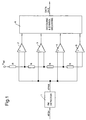
- FIG. 1 shows the circuit diagram of the comparator-detection, which is traditionally used as the detection method in prior art paging systems.
- the incoming signal is modulated by 4 level frequency shift keying (4FSK), said modulated signal is received in the FM detection block 1.
- the FM detected and 4 level pulse amplitude modulated (4PAM) signal is supplied to the inputs of comparator-detectors (2 - 5), in which the signal is compared with fixed decision levels. The comparison result is the information about which symbol was received.
- the outputs of the comparators are connected to the decoding & symbol decoding block 6, which provides the outgoing data.
- a digital detector to convert an analog signal into a digital signal is known for example from US-A-4 873 702
- a digital detector to convert an audio frequency signal into a digital signal
- the detector comprises, an Analogue/Digital (A/D) converter (7), for producing a first binary word (W 0 ) corresponding to the offset voltage of the detector, and a second binary word (W s ) corresponding to each detected signal, offset voltage removal means (8), in which the first binary word (W o ) corresponding to the offset voltage of the detector is subtracted from each second binary word (W s ) corresponding to each received signal to provide a plurality of third binary words (W ss ) representing modified signal symbols corresponding to each received signal, means for comparing each third binary word (W ss ) with a set of predetermined decision levels to determine an output symbol and, means for updating the set of predetermined decision levels responsive to changes in the received audio frequency signals as represented in changes in the third binary words (W ss ).
- A/D Analogue/Digital
- a method for operating a digital detector for converting an audio frequency signal into a digital signal comprising the steps of producing a first binary word (W o ) corresponding to an offset voltage of the detector and a second binary word (W s ) corresponding to each detected signal; subtracting the first binary word (W o ) from each second binary word (W s ) to provide a plurality of third binary words (W ss ) representing modified signal symbols corresponding to each received signal; comparing each third binary word (W ss ) with a set of predetermined decision levels to determine an output symbol; and updating the set of predetermined decision levels in response to a change in the received audio frequency signals as represented by a change in the third binary words (W ss ).
- a disadvantage of detectors with fixed levels, which is overcome by the present invention, is that their decision levels must be manually tuned in order to provide the best detection result.
- Figure 2 shows a block diagram of the decision logic of the signal detector in accordance with the invention.
- the 4FSK modulated signal is detected with the FM detector, then the different voltage values are converted into digital ones with the A/D-converter 7. It is not necessary to scale the output of the A/D-converter 7 in any special way, if the conversion range is selected so that no overflow will occur.
- the radio In the beginning of every connection the radio is switched on before the data reception is started. During this time the receiver can be synchronized with the incoming data flow.
- the binary word w 0 corresponding to the offset voltages of the radio, the mixer and particularly of the FM detector can be read from the A/D-converter 7. This binary word w 0 is supplied to the logic, which reads and stores it in the register block 9 into a register allocated for it.
- the register block 9 contains also the decision levels and the alarm levels.
- An adder 10 is also connected to the register block 9.
- the 8-bit digital comparator 11 compares each input binary word w s with the decision levels and the alarm levels.
- the updating logic 12 updates the decision levels and the alarm levels.
- the symbol decoding logic 13 outputs serial data.
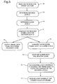
- Figure 3 shows a function diagram of the decision logic of the signal detector according to the invention.
- the decision level determination function 15 of the decision logic determines a new decision level l 1 , l 2 and l 3 corresponding to each symbol.
- the determination 15 of the symbol decision levels will be successful, because there is a so called preamble in the synchronizing part at the beginning of each batch of the protocol, the preamble containing only symbols "10" and "00". These symbols correspond to the extremes of a 4FSK modulated signal, so that the voltage values from the FM detector always correspond to the lowest l 1 and to the highest l 3 symbol decision level.
- the voltage values from the FM detector are converted into binary words.
- the midmost decision level l 2 is simply the mean value of the former decision levels l 1 and l 3 . Calculation of the midmost decision level is easily realized with the aid of digital addition and shifting of the sum in the shift register.
- the alarm level determination function 16 determines certain alarm levels, so that the symbol decision levels can be changed due to changes in the conditions or changes in the signal. This is a prerequisite to continue error free reception of a message, when the pager moves with different speeds during the same connection.
- the signal frequencies change with respect to the pager, when the pager moves with varying speeds. This can be explained with the Doppler-effect.
- the decision logic is ready to receive a call.
- the beginning of the call there is an address. If the pager identifies the address as being its own and finds that a call is arriving, the function continues. In the opposite case the connection is ended and the function continues at the beginning of a new connection.
- Each message or signal symbol binary word w ss is in the comparison device 17 compared with the symbol decision levels l 3 , l 2 and l 1 .
- the comparison device 17 compares the absolute values of two binary words, or it compares the value of the respective word if it would be converted into a number of the decimal system. If the received word w s is greater than the decision level l 3 , it will know that the received symbol was "10". If the received word w s is smaller than the decision level l 3 , the decision level l 2 will be loaded into the comparison device. Then there is examined whether the absolute value of the word w ss is greater than the absolute value of the decision level l 2 , and if so, then the received symbol is "11".
- the decision level l 1 will be loaded into the comparison device. Then there is examined whether the absolute value of the word W ss is greater than the absolute value of the decision level l 1 , and if so, then the received symbol is "01". If the absolute value of the word W ss is smaller than the decision level, then the received symbol is "00". In this way the symbol decoding logic 18 is able to output correct data from the decision logic.
- the updating logic calculates from the symbol decision levels an alarm level 19 for each symbol decision level according to a predetermined algorithm.
- the binary word w s representing a received symbol is smaller than the lower alarm level l a of the detected symbol or greater than the upper alarm level l h of the detected symbol, then the updating logic will observe 20 the alarm which occurred.
- the symbol decision levels are changed 21 to reflect the new situation.
- the alarm levels are changed 16 in accordance with the change of symbol decision levels.
- the symbol decision levels and the alarm levels are changed before the next symbol is received.
- the symbol reception is continued in a normal way, and again the symbol levels are first compared 17 and 19 with the levels in the logic.
- the detector is able to remove the individual differences of the pager front end before the detection, in other words, the digital detector will see a front end with similar electrical characteristics, even when the component characteristics change in different pager units.
- the digital detector will identify changes of the signalling frequencies, which occur in the transmission channel, and it is able to react on these. In this way the reception of a message can be continued substantially without errors, even though the signalling frequencies which correspond to the different symbols would change.
- the invention can be realized in hardware or with a microprocessor.
- the hardware embodiment is preferred, because the detector is a lasting construction, which does not require modifications, and the microprocessor capacity can more effectively be used in other functions.
Landscapes
- Engineering & Computer Science (AREA)
- Power Engineering (AREA)
- Computer Networks & Wireless Communication (AREA)
- Signal Processing (AREA)
- Mobile Radio Communication Systems (AREA)
- Digital Transmission Methods That Use Modulated Carrier Waves (AREA)
Claims (12)
- Digitaler Detektor zur Umwandlung eines Audiofrequenzsignals in ein digitales Signal, gekennzeichnet durch:- einen Analog/Digital (A/D) Wandler (7) zur Bildung eines ersten mit der Offset-Spannung des Detektors korrespondierenden binären Wortes (W0) und eines zweiten mit jedem einzelnen detektierten Signal korrespondierenden binären Wortes (WS);- Mittel (8) zum Beseitigen der Offset-Spannung, in denen das erste mit der Offset-Spannung des Detektors korrespondierende binäre Wort (W0) von jedem zweiten mit jedem einzelnen empfangenen Signal korrespondierenden binären Wort (WS) subtrahiert wird, um eine Vielzahl von dritten binären Wörtern (WSS) zu liefern, die für modifizierte Signalsymbole stehen, welche mit jedem einzelnen empfangenen Signal korrespondieren;- Mittel zum Vergleichen des jedes dritten binären Worts (WSS) mit einem Satz vorbestimmter Entscheidungsschwellenwerte, um ein Ausgangssymbol zu bestimmen; und- Mittel zum Aktualisieren des vorbestimmten Satzes von Entscheidungsschwellenwerten in Antwort auf Änderungen der empfangenen Audiofrequenzsignale, wie sie durch Änderungen in den dritten binären Wörtern (WSS) repräsentiert werden.
- Digitaler Detektor nach Anspruch 1, bei dem die Mittel (12) zur Aktualisierung des Satzes an vorbestimmten Entscheidungsschwellenwerten auf das dritte binäre Wort (WSS) ansprechen, falls dieses eine vorbestimmte Anzahl von Malen außerhalb einer vorbestimmten Zone liegt, die durch einen oberen und unteren Alarmpegel (la, lh) definiert ist.
- Digitaler Detektor nach Anspruch 1, bei dem jedesmal, wenn ein neues Signal vom Detektor empfangen wird, die Mittel zur Aktualisierung des Satzes an vorbestimmten Entscheidungsschwellenwerten einen neuen Satz von Entscheidungsschwellenwerten (11, 12 und 13) bestimmen, die mit jedem neuen Signal korrespondieren.
- Digitaler Detektor nach Anspruch 3, bei dem jedes Signal einen einleitenden Teil aufweist, der dazu benutzt wird, den neuen Satz an Entscheidungsschwellenwerten zu bestimmen, wobei der einleitende Teil nur die Symbole "10" und "00" enthält, die mit den Extremwerten eines mittels Vierfach-Frequenzumtastung (4FSK) modulierten Signals korrespondieren.
- Digitaler Detektor nach Anspruch 3, bei dem die Mittel zur Aktualisierung des Satzes vorbestimmter Entscheidungsschwellenwerte ein Summenregister für jedes Symbol im Register (9) enthalten, wobei der Inhalt des Registers wechselweise zur Berechnung einer Summe in einen Addierer geladen wird.
- Digitaler Detektor nach irgendeinem vorangegangenen Anspruch, bei dem die Entscheidungsschwellenwerte 11 und 13 aufgrund des Durchschnittswertes von vier Abtastwerten durch Schieben der Daten im Schieberegister um 2 Bit in Richtung des am wenigsten signifikanten Bits bestimmt werden, sowie durch Laden des binären Symbols "0" in die leeren Flip-Flops des Schieberegisters, wobei der mittlere Entscheidungsschwellenwert 12 als Mittelwert der früheren Entscheidungsschwellenwerte 11 und 13 berechnet wird.
- Digitaler Detektor nach irgendeinem vorangegangenen Anspruch, bei dem die Mittel zur Aktualisierung des vorbestimmten Satzes an Entscheidungsschwellenwerten das dritte binäre Wort (WSS), das irgendeinen der Alarmpegel (la oder lh) in einer bestimmten Richtung ausreichend oft überschreitet, detektieren, so daß sich dann die Symbolentscheidungswerte (21) und die Alarmpegel (16) ändern, um die Änderungen im dritten binären Wort (WSS) widerzuspiegeln, bevor das nächste Symbol empfangen wird.
- Verfahren zum Betrieb eines digitalen Detektors zwecks Umwandlung eines Audiofrequenzsignals in ein digitales Signal, mit folgenden Schritten:- Bildung eines ersten binären Worts (W0), das mit einer Offset-Spannung des Detektors korrespondiert, und eines zweiten binären Worts (WS), das mit jedem detektierten Signal korrespondiert;- Subtraktion des ersten binären Worts (W0) von jedem zweiten binären Wort (WS), um eine Vielzahl von dritten binären Wörtern (WSS) zu bilden, die modifizierte Signalsymbole repräsentieren, welche mit jedem empfangenen Signal korrespondieren;- Vergleichen eines jeden dritten binären Worts (WSS) mit einem Satz vorbestimmter Entscheidungsschwellenwerte, um ein Ausgangssymbol zu bestimmen; und- Aktualisieren des Satzes vorbestimmter Entscheidungsschwellenwerte in Antwort auf die Änderung der empfangenen Audiofrequenzsignale, symbolisiert durch eine Änderung der dritten binären Wörter (WSS).
- Verfahren nach Anspruch 8, bei dem der Aktualisierungsschritt einen Bestimmungsschritt enthält, falls das dritte binäre Wort (WSS) eine vorbestimmte Anzahl von Malen außerhalb einer vorbestimmten Zone liegt, die durch einen oberen und unteren Alarmpegel (la, lh) definiert ist.
- Verfahren nach Anspruch 8, bei dem der Aktualisierungsschritt auf ein neues Signal reagiert, das zur Bestimmung eines neuen Satzes an Entscheidungsschwellenwerten (11, 12 und 13), die mit jedem neuen Signal korrespondieren, empfangen wurde.
- Verfahren nach Anspruch 10, bei dem der Schritt zur Bestimmung eines neuen Satzes an Entscheidungsschwellenwerten auf einen einleitenden Teil eines jeden Signals reagiert, wobei der einleitende Teil nur die Symbole "10" und "00" enthält, die mit den Extremwerten eines mittels Vierfach-Frequenzumtastung (4FSK) modulierten Signals korrespondieren.
- Verfahren nach irgendeinem der Ansprüche 8 bis 11, bei dem der Aktualisierungsschritt einen Schritt zur Detektierung des dritten binären Wortes (WSS) enthält, das irgendeinen der Alarmpegel (la, lh) in einer bestimmten Richtung ausreichend oft überschreitet, und einen Schritt zur Änderung der Symbolentscheidungswerte (21) und der Alarmpegel (16) aufweist, um Änderungen im dritten binären Wort (WSS) widerzuspiegeln, bevor ein nächstes Symbol empfangen wird.
Applications Claiming Priority (2)
| Application Number | Priority Date | Filing Date | Title |
|---|---|---|---|
| FI915179A FI89437C (fi) | 1991-11-01 | 1991-11-01 | Digitaldetektor foer ett soekaranlaeggningsystem |
| FI915179 | 1991-11-01 |
Publications (3)
| Publication Number | Publication Date |
|---|---|
| EP0540359A2 EP0540359A2 (de) | 1993-05-05 |
| EP0540359A3 EP0540359A3 (en) | 1993-06-30 |
| EP0540359B1 true EP0540359B1 (de) | 1997-01-08 |
Family
ID=8533415
Family Applications (1)
| Application Number | Title | Priority Date | Filing Date |
|---|---|---|---|
| EP92309972A Expired - Lifetime EP0540359B1 (de) | 1991-11-01 | 1992-10-30 | Adaptiver Pegeldetektor |
Country Status (4)
| Country | Link |
|---|---|
| US (1) | US5287540A (de) |
| EP (1) | EP0540359B1 (de) |
| DE (1) | DE69216553T2 (de) |
| FI (1) | FI89437C (de) |
Families Citing this family (7)
| Publication number | Priority date | Publication date | Assignee | Title |
|---|---|---|---|---|
| JP2639326B2 (ja) * | 1993-11-30 | 1997-08-13 | 日本電気株式会社 | 四値fsk受信機 |
| US5446771A (en) * | 1994-01-24 | 1995-08-29 | Motorola, Inc. | Adaptive coherent signal detection method and apparatus |
| US5825243A (en) * | 1995-10-30 | 1998-10-20 | Casio Computer Co., Ltd. | Apparatus and method for demodulating multi-level signal |
| US5761259A (en) * | 1996-05-24 | 1998-06-02 | International Business Machines Corporation | Apparatus, method and article of manufacture for carrier frequency compensation in a FM radio |
| CN1119021C (zh) * | 1996-06-25 | 2003-08-20 | 英国电讯有限公司 | 多级别数字数据传输系统和接收器 |
| GB9613228D0 (en) * | 1996-06-25 | 1996-08-28 | British Telecomm | Data transmission |
| JP3655770B2 (ja) * | 1999-03-29 | 2005-06-02 | 日本電気株式会社 | 光受信回路 |
Family Cites Families (10)
| Publication number | Priority date | Publication date | Assignee | Title |
|---|---|---|---|---|
| US3860874A (en) * | 1973-12-04 | 1975-01-14 | Us Interior | Receiver for dfsk signals |
| US4086430A (en) * | 1975-11-14 | 1978-04-25 | Motorola, Inc. | Detection circuitry |
| NL8200051A (nl) * | 1982-01-08 | 1983-08-01 | Philips Nv | Inrichting en werkwijze voor het detecteren van multifrequentie tooncodesignalen. |
| JPS60174550A (ja) * | 1984-02-21 | 1985-09-07 | Nippon Telegr & Teleph Corp <Ntt> | 符号再生回路 |
| US4554509A (en) * | 1984-08-27 | 1985-11-19 | Hrb-Singer, Inc. | Frequency shift keyed demodulation system |
| JPS6468162A (en) * | 1987-09-09 | 1989-03-14 | Man Design Co | Fsk demodulator |
| JPS6468161A (en) * | 1987-09-09 | 1989-03-14 | Man Design Co | Fsk demodulator |
| US4873702A (en) * | 1988-10-20 | 1989-10-10 | Chiu Ran Fun | Method and apparatus for DC restoration in digital receivers |
| WO1991005427A1 (en) * | 1989-09-29 | 1991-04-18 | Motorola, Inc. | Method of dc offset compensation using a transmitted dc compensation signal |
| US5204879A (en) * | 1991-01-31 | 1993-04-20 | Motorola, Inc. | High speed data detection and clock recovery in a received multi-level data signal |
-
1991
- 1991-11-01 FI FI915179A patent/FI89437C/fi not_active IP Right Cessation
-
1992
- 1992-10-28 US US07/967,512 patent/US5287540A/en not_active Expired - Lifetime
- 1992-10-30 DE DE69216553T patent/DE69216553T2/de not_active Expired - Fee Related
- 1992-10-30 EP EP92309972A patent/EP0540359B1/de not_active Expired - Lifetime
Also Published As
| Publication number | Publication date |
|---|---|
| EP0540359A3 (en) | 1993-06-30 |
| EP0540359A2 (de) | 1993-05-05 |
| DE69216553T2 (de) | 1997-06-12 |
| FI89437C (fi) | 1993-09-27 |
| FI915179A0 (fi) | 1991-11-01 |
| US5287540A (en) | 1994-02-15 |
| FI89437B (fi) | 1993-06-15 |
| DE69216553D1 (de) | 1997-02-20 |
Similar Documents
| Publication | Publication Date | Title |
|---|---|---|
| US5949827A (en) | Continuous integration digital demodulator for use in a communication device | |
| US5157672A (en) | Interference detection apparatus for use in digital mobile communications system | |
| EP0108938B1 (de) | Digitale Rufanlage mit Bit-Geschwindigkeitsumschalter und zugehöriger digitaler Empfänger | |
| US5425056A (en) | Method and apparatus for generating threshold levels in a radio communication device for receiving four-level signals | |
| EP0400983B1 (de) | Bitfehlerratenerkennung | |
| US5566213A (en) | Selective call receiving device with improved symbol decoding and automatic frequency control | |
| US6226505B1 (en) | Automatic frequency correction apparatus and method for radio calling system | |
| EP0540359B1 (de) | Adaptiver Pegeldetektor | |
| US6456831B1 (en) | Amplitude change time activated phase locked controller in a selective call receiver | |
| US4302817A (en) | Digital Pseudo continuous tone detector | |
| US5561665A (en) | Automatic frequency offset compensation apparatus | |
| JPH09205466A (ja) | シンボル判定装置 | |
| EP0081499B1 (de) | Durch daten aktivierte rauschsperre | |
| US4224689A (en) | Apparatus for smoothing transmission errors | |
| US5724389A (en) | Method and apparatus for detecting a presence of a predetermined baud rate | |
| US6359942B1 (en) | FSK demodulator | |
| US4509180A (en) | Method and an apparatus for correcting distortion of binary received signals | |
| US5564091A (en) | Method and apparatus for operating an automatic frequency control in a radio | |
| US5425053A (en) | Radio communication apparatus which can quickly recover from misjudgement of levels of a multilevel modulated signal | |
| JPH11127207A (ja) | デジタル無線通信装置の検波方法及びその回路 | |
| JP2000349840A (ja) | ベースバンド信号オフセット補正回路及び方法、この補正回路を備えたfsk受信装置 | |
| CA1278049C (en) | Digital circuit extracting synchronism signals from a serial flow of coded data | |
| US5768321A (en) | Automatic frequency control unit which detects a frame pattern in a phase modulation signal | |
| US6232906B1 (en) | Quaternary FSK receiver and method of judging signals in quaternary FSK receiver | |
| CA1266515A (en) | Start pattern detecting apparatus |
Legal Events
| Date | Code | Title | Description |
|---|---|---|---|
| PUAI | Public reference made under article 153(3) epc to a published international application that has entered the european phase |
Free format text: ORIGINAL CODE: 0009012 |
|
| AK | Designated contracting states |
Kind code of ref document: A2 Designated state(s): CH DE FR GB LI NL SE |
|
| PUAL | Search report despatched |
Free format text: ORIGINAL CODE: 0009013 |
|
| AK | Designated contracting states |
Kind code of ref document: A3 Designated state(s): CH DE FR GB LI NL SE |
|
| 17P | Request for examination filed |
Effective date: 19930807 |
|
| GRAG | Despatch of communication of intention to grant |
Free format text: ORIGINAL CODE: EPIDOS AGRA |
|
| 17Q | First examination report despatched |
Effective date: 19960124 |
|
| GRAH | Despatch of communication of intention to grant a patent |
Free format text: ORIGINAL CODE: EPIDOS IGRA |
|
| GRAH | Despatch of communication of intention to grant a patent |
Free format text: ORIGINAL CODE: EPIDOS IGRA |
|
| GRAA | (expected) grant |
Free format text: ORIGINAL CODE: 0009210 |
|
| AK | Designated contracting states |
Kind code of ref document: B1 Designated state(s): CH DE FR GB LI NL SE |
|
| REG | Reference to a national code |
Ref country code: CH Ref legal event code: NV Representative=s name: E. BLUM & CO. PATENTANWAELTE Ref country code: CH Ref legal event code: EP |
|
| ET | Fr: translation filed | ||
| REF | Corresponds to: |
Ref document number: 69216553 Country of ref document: DE Date of ref document: 19970220 |
|
| PLBE | No opposition filed within time limit |
Free format text: ORIGINAL CODE: 0009261 |
|
| 26N | No opposition filed | ||
| REG | Reference to a national code |
Ref country code: GB Ref legal event code: IF02 |
|
| REG | Reference to a national code |
Ref country code: GB Ref legal event code: 732E |
|
| PGFP | Annual fee paid to national office [announced via postgrant information from national office to epo] |
Ref country code: FR Payment date: 20031003 Year of fee payment: 12 |
|
| PGFP | Annual fee paid to national office [announced via postgrant information from national office to epo] |
Ref country code: SE Payment date: 20031007 Year of fee payment: 12 |
|
| PGFP | Annual fee paid to national office [announced via postgrant information from national office to epo] |
Ref country code: NL Payment date: 20031008 Year of fee payment: 12 |
|
| PGFP | Annual fee paid to national office [announced via postgrant information from national office to epo] |
Ref country code: GB Payment date: 20031029 Year of fee payment: 12 |
|
| PGFP | Annual fee paid to national office [announced via postgrant information from national office to epo] |
Ref country code: CH Payment date: 20031030 Year of fee payment: 12 |
|
| PGFP | Annual fee paid to national office [announced via postgrant information from national office to epo] |
Ref country code: DE Payment date: 20031103 Year of fee payment: 12 |
|
| PG25 | Lapsed in a contracting state [announced via postgrant information from national office to epo] |
Ref country code: GB Free format text: LAPSE BECAUSE OF NON-PAYMENT OF DUE FEES Effective date: 20041030 |
|
| PG25 | Lapsed in a contracting state [announced via postgrant information from national office to epo] |
Ref country code: SE Free format text: LAPSE BECAUSE OF NON-PAYMENT OF DUE FEES Effective date: 20041031 Ref country code: LI Free format text: LAPSE BECAUSE OF NON-PAYMENT OF DUE FEES Effective date: 20041031 Ref country code: CH Free format text: LAPSE BECAUSE OF NON-PAYMENT OF DUE FEES Effective date: 20041031 |
|
| PG25 | Lapsed in a contracting state [announced via postgrant information from national office to epo] |
Ref country code: NL Free format text: LAPSE BECAUSE OF NON-PAYMENT OF DUE FEES Effective date: 20050501 |
|
| PG25 | Lapsed in a contracting state [announced via postgrant information from national office to epo] |
Ref country code: DE Free format text: LAPSE BECAUSE OF NON-PAYMENT OF DUE FEES Effective date: 20050503 |
|
| EUG | Se: european patent has lapsed | ||
| REG | Reference to a national code |
Ref country code: CH Ref legal event code: PL |
|
| GBPC | Gb: european patent ceased through non-payment of renewal fee |
Effective date: 20041030 |
|
| PG25 | Lapsed in a contracting state [announced via postgrant information from national office to epo] |
Ref country code: FR Free format text: LAPSE BECAUSE OF NON-PAYMENT OF DUE FEES Effective date: 20050630 |
|
| NLV4 | Nl: lapsed or anulled due to non-payment of the annual fee |
Effective date: 20050501 |
|
| REG | Reference to a national code |
Ref country code: FR Ref legal event code: ST |