EP0539794B1 - Spatial light modulator laser dot scanner - Google Patents
Spatial light modulator laser dot scanner Download PDFInfo
- Publication number
- EP0539794B1 EP0539794B1 EP92117473A EP92117473A EP0539794B1 EP 0539794 B1 EP0539794 B1 EP 0539794B1 EP 92117473 A EP92117473 A EP 92117473A EP 92117473 A EP92117473 A EP 92117473A EP 0539794 B1 EP0539794 B1 EP 0539794B1
- Authority
- EP
- European Patent Office
- Prior art keywords
- light
- pixels
- light modulator
- mirror
- rows
- Prior art date
- Legal status (The legal status is an assumption and is not a legal conclusion. Google has not performed a legal analysis and makes no representation as to the accuracy of the status listed.)
- Expired - Lifetime
Links
Images


Classifications
-
- G—PHYSICS
- G06—COMPUTING OR CALCULATING; COUNTING
- G06K—GRAPHICAL DATA READING; PRESENTATION OF DATA; RECORD CARRIERS; HANDLING RECORD CARRIERS
- G06K7/00—Methods or arrangements for sensing record carriers, e.g. for reading patterns
- G06K7/10—Methods or arrangements for sensing record carriers, e.g. for reading patterns by electromagnetic radiation, e.g. optical sensing; by corpuscular radiation
- G06K7/10544—Methods or arrangements for sensing record carriers, e.g. for reading patterns by electromagnetic radiation, e.g. optical sensing; by corpuscular radiation by scanning of the records by radiation in the optical part of the electromagnetic spectrum
- G06K7/10554—Moving beam scanning
- G06K7/10594—Beam path
- G06K7/10683—Arrangement of fixed elements
- G06K7/10702—Particularities of propagating elements, e.g. lenses, mirrors
-
- G—PHYSICS
- G02—OPTICS
- G02B—OPTICAL ELEMENTS, SYSTEMS OR APPARATUS
- G02B26/00—Optical devices or arrangements for the control of light using movable or deformable optical elements
- G02B26/08—Optical devices or arrangements for the control of light using movable or deformable optical elements for controlling the direction of light
- G02B26/10—Scanning systems
-
- G—PHYSICS
- G06—COMPUTING OR CALCULATING; COUNTING
- G06K—GRAPHICAL DATA READING; PRESENTATION OF DATA; RECORD CARRIERS; HANDLING RECORD CARRIERS
- G06K7/00—Methods or arrangements for sensing record carriers, e.g. for reading patterns
- G06K7/10—Methods or arrangements for sensing record carriers, e.g. for reading patterns by electromagnetic radiation, e.g. optical sensing; by corpuscular radiation
- G06K7/10544—Methods or arrangements for sensing record carriers, e.g. for reading patterns by electromagnetic radiation, e.g. optical sensing; by corpuscular radiation by scanning of the records by radiation in the optical part of the electromagnetic spectrum
- G06K7/10554—Moving beam scanning
- G06K7/10594—Beam path
Definitions
- This invention relates to scanning of images, more particularly to a method for scanning an object by using a spatial light modulator.
- the light source is some type of laser.
- the mirror is a rotating polygonal solid which scans a dot of light along a linear axis.
- the bar code has a white area, there is a low level of light returned, since white paper is a light diffuser. But when the light dot hits a black bar, the light level drops. This drop off signals the unit to do some simple processing. It counts the increment of time for which there is no return light.
- a thick black bar may be six or seven increments, a thin one only one or two.
- JP-A-02124142 a scanning system is disclosed using stripes on a liquid crystal panel. The addressing of these stripes will not allow fast scanning.
- JP-A-63049892 also discloses a scanning system with a liquid crystal panel with stripes of the same type as disclosed in the before-mentioned document.
- US-A-4 596 992 a printer is disclosed which uses a linear spatial light modulator to form an image on a photosensitive drum. The modulator forms the image in its entirety across the device for a particular line to be exposed on the drum, then the face of the modulator, configured in the desired image, is exposed to transfer that image to the drum. This printer is not really a scanning system.
- an optical scanner which comprises a plurality of reflective elements arranged side by side in one row, each element being supported by arms, the arms and the reflective elements being micro-machined.
- the depth of the reflective elements relative to the plane of the face of the scanner is adjustable, so that there is a progressive phase shift between an incident plane wavefront and the respective reflecting surfaces.
- JP-A-62035323 an optical system is disclosed forming an image on a screen.
- the optical system comprises a DMD having two offset rows of pixels. There is no mention of address timing of the pixels.
- the present invention provides a method for image scanning as defined in the claim.
- the image is scanned by activating one pixel at a time along the line of SLM cells to replace the function of the moving mirror in conventional scanners.
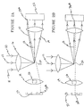
- FIGURE 1 shows a scanning system including a spatial light modulator in its inactive state for a Schlieren optical system.
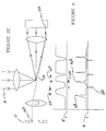
- FIGUREs 2A-2C shows the light rays as individual pixels are activated at the start, middle and end of the device for a Schlieren optical system.
- FIGURE 3A shows a scanning system including a spatial light modulator and dark field optics.
- FIGURE 3B shows a dark field optics scanning system folded to fit in a hand held scanning unit.
- FIGURE 4 shows representations of the data received by the detector and the processed result.
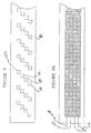
- FIGURE 5 shows a staggered arrangement of pixels on a spatial light modulator.
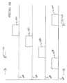
- FIGURE 6A shows a possible data flow through addressing shift registers.
- FIGURE 6B shows a timing diagram for a data flow through addressing shift registers.
- Figure 1 shows a top view of a scanning system that does not use a moving mirror, in its inactive state.
- Rays 10, 12 and 14, respectively, will illuminate the right side, the middle and the left side of the modulator.
- the light from the source is passed through lens 16, which focuses the three rays onto the stationary, tilted, stop mirror 18.
- Stop mirror 18 reflects and separates the rays to pass them through lens element 20.
- Lens element 20 is arranged to achieve the opposite effect of element 16, as it collimates the rays and passes them to the spatial light modulator array 22. In this instance, none of the pixels of the array are activated.
- the only requirement for the spatial light modulator in its inactive state is that it reflects the rays back along the same path they arrived through. In this state, the stop mirror works to prevent any of the illumination from reaching the lens element 24, which has detector 26 mounted above it. The detector does not necessarily need to be mounted there. Its only requirement is that it must be able to detect reflections from the object being scanned.
- An array of pixels may be 1000 pixels long.
- the use of the three example pixels is to show three areas of interest on the device. It is not meant to be implied that only three such pixels are used.
- Figure 2A shows how the object, such as a bar code, is scanned.
- the requirement for the spatial light modulator now changes. To scan the image in this part of the system, the spatial light modulator must be able to reflect the outgoing beam to a different path from the incoming path. Additionally, the SLM must be able to do this one pixel at a time.
- the DMD consists of an array of micromechanical mirrors suspended on hinges over an air gap. At the bottom of the air gap, underneath the mirrors, is an array of electrodes for addressing the mirrors. When the electrode has charge placed upon it, the mirror over that electrode deflects to an angle that will allow it to direct light back along a different path.
- the light rays 10, 12, and 14 travel the same paths previously discussed. But, this time when the rays pass through the lens to the SLM, pixel 28A, where ray 10 is to impinge upon the array, is deflected at an angle. The pixels where rays 12 and 14 impinge and all other pixels, not shown, are not deflected.
- the deflected beam 30 now carries the light that was previously in beam 10. Because of its new path, beam 30 misses the stop mirror 18 and travels through to lens element 26. The light then impinges upon a bar code, or object, for the supermarket or department store scanner, which then reflects diffuse light back to the detector, since the spot 28B is on a white bar. Only the light reflected by point 28B, corresponding to pixel 28A, will be seen by the detector.
- White is represented by a raised area on the object 25, and black by the holes between the raised areas.
- Figure 2B the same thing is repeated for the middle of the image, in beam 12.
- This time pixel 36A is deflected, while all other pixels are flat, and deflected beam 32 is directed away from the stop mirror 18.
- Ray 32 then passes through the lens 26 and reflects a lower level of light, since point 36B is on a black spot, to detector 24.
- Figure 2C shows the same process for the left edge of the image in beam 14. Beam 14 impinges upon deflected pixel 38A and is reflected into beam 34. Beam 34 then passes through the lens 26 and impinges upon the bar code or object at point 38B.
- Figure 3A shows a further embodiment of the scanning system, using dark field optics.
- light source 9 directs light through lens 11, via beams 10, 12, and 14, to the spatial light modulator 22. If any of the pixels 28A, 36A, or 38A are deflected, the light would travel along paths 30, 32 or 34, respectively. Light from the undeflected pixels would travel along the group of paths 29 as unused light. Reflected light passes through the dark field optics system 48 and impinges upon object 25. The detector, not shown, could be placed anywhere in the proximity of object 25 to receive light levels reflected from the object.
- Schlieren optics or dark field optics is up to the designer, as are the selection of any other types of optics.
- Schlieren optics require an inherent trade-off between signal strength and dynamic range, while dark field optics, if appropriate can provide both large signal and wide dynamic range. Additionally, any selected optics may require a long optical axis. This problem can be avoided as shown in Figure 3B.
- FIG 3B the optical path of the previous dark field optics, shown in Figure 3A is folded. This is particularly useful in the hand held unit, where the size is a restriction upon the design.
- Light source 9 provides illumination through lens 11.
- the path of this illumination is folded by fold mirror 15, which then passes the light to the SLM 22. Again reflected light passes in the direction shown by paths 30, 32, and 34. Unused light travels along path 29.
- Light reflected from the SLM passes through the optics 48 and impinges upon object 25.
- the fold mirror could be located just behind the trigger guard, the light source would then be in the bottom of the hand grip, the SLM at one end of the barrel and the light would exit at the other end.
- the switch which activates the light source and the SLM most likely, a pressure switch in the hand held unit.
- the light source is always on, but the system only registers scans when there is an object presented to it.
- Figure 4 shows the information being detected and how that information is translated into a bar code.
- Line 40 contains the information at the detector. The light beams being deflected along a line of the image impinge upon the bar code.
- the detector "sees" the segment 42A.
- the bar code has a black bar, which reflects a lower level of light back to the detector.
- segment 46A there is a white bar.
- the resulting information after processing is seen on line 41.
- Spike 42B signals that it is the beginning of a white bar.
- Spike 44B shows the beginning of a black bar.
- the processor then counts the number of pixels between the falling edge of spike 44B and the leading edge of spike 46B to record the width of the black bar. This process continues until the entire length of the bar code has been scanned. This data is then converted to some product number and the price is sent to the cash register.
- DMDs have an advantage in that they are very small. Staggering rows of the mirror as seen in Figure 5 can increase the speed to match the fastest detector.
- FIG 5 a staggered arrangement of pixels is shown on spatial light modulator 22. Pixels 50A-50D are of particular interest, when viewed in light of Figure 6.
- Figure 6 shows a possible implementation of addressing circuitry for a deformable mirror device (DMD). In reality, addressing circuitry shown in Figure 6A would be underneath the mirrors shown in Figure 5.
- DMD deformable mirror device
- FIG. 6B The timing of clock signal lines 52A-52D is shown in Figure 6B.
- Line 54A shows the one seen in Figure 6A for mirror 50A of Figure 5.
- the data is clocked in to the cell of the address register that is directly below pixel 50A during time segment 56, which is 2.5 ⁇ secs long. While that mirror is in its switching time of 10 ⁇ secs, the next pixel, 50B, is clocked with data, seen on line 54B, pulse 58B. This continues until all four pixels have been clocked with data.
- pixel 50D After pixel 50D has received pulse 58D seen on line 54D, pixel 50A can again receive data. It is clocked with pulse 60A.
- the time difference between the leading edge of pulse 58A and pulse 60A is shown by time segment 62. It is 10 ⁇ secs long.
- time segment 62 It is 10 ⁇ secs long.
- This method of scanning makes it faster than conventional scanning. Regardless of what timing scheme is used, this scanner is lighter, smaller, and uses less power, due to the elimination of the spinning mirror, and the motor or coil used to drive it.
Landscapes
- Physics & Mathematics (AREA)
- Engineering & Computer Science (AREA)
- Electromagnetism (AREA)
- General Physics & Mathematics (AREA)
- Toxicology (AREA)
- General Health & Medical Sciences (AREA)
- Health & Medical Sciences (AREA)
- Artificial Intelligence (AREA)
- Computer Vision & Pattern Recognition (AREA)
- Theoretical Computer Science (AREA)
- Optics & Photonics (AREA)
- Mechanical Optical Scanning Systems (AREA)
- Facsimile Scanning Arrangements (AREA)
- Mechanical Light Control Or Optical Switches (AREA)
- Length Measuring Devices By Optical Means (AREA)
Applications Claiming Priority (2)
| Application Number | Priority Date | Filing Date | Title |
|---|---|---|---|
| US07/786,162 US5563398A (en) | 1991-10-31 | 1991-10-31 | Spatial light modulator scanning system |
| US786162 | 1991-10-31 |
Publications (2)
| Publication Number | Publication Date |
|---|---|
| EP0539794A1 EP0539794A1 (en) | 1993-05-05 |
| EP0539794B1 true EP0539794B1 (en) | 1998-01-21 |
Family
ID=25137769
Family Applications (1)
| Application Number | Title | Priority Date | Filing Date |
|---|---|---|---|
| EP92117473A Expired - Lifetime EP0539794B1 (en) | 1991-10-31 | 1992-10-13 | Spatial light modulator laser dot scanner |
Country Status (7)
| Country | Link |
|---|---|
| US (1) | US5563398A (enExample) |
| EP (1) | EP0539794B1 (enExample) |
| JP (1) | JP3164442B2 (enExample) |
| KR (1) | KR100247145B1 (enExample) |
| CA (1) | CA2079499C (enExample) |
| DE (1) | DE69224139T2 (enExample) |
| TW (1) | TW228576B (enExample) |
Families Citing this family (173)
| Publication number | Priority date | Publication date | Assignee | Title |
|---|---|---|---|---|
| US6674562B1 (en) | 1994-05-05 | 2004-01-06 | Iridigm Display Corporation | Interferometric modulation of radiation |
| US6467345B1 (en) | 1993-10-18 | 2002-10-22 | Xros, Inc. | Method of operating micromachined members coupled for relative rotation |
| US6044705A (en) * | 1993-10-18 | 2000-04-04 | Xros, Inc. | Micromachined members coupled for relative rotation by torsion bars |
| US7123216B1 (en) | 1994-05-05 | 2006-10-17 | Idc, Llc | Photonic MEMS and structures |
| US8014059B2 (en) | 1994-05-05 | 2011-09-06 | Qualcomm Mems Technologies, Inc. | System and method for charge control in a MEMS device |
| US7138984B1 (en) | 2001-06-05 | 2006-11-21 | Idc, Llc | Directly laminated touch sensitive screen |
| US7460291B2 (en) | 1994-05-05 | 2008-12-02 | Idc, Llc | Separable modulator |
| US6680792B2 (en) | 1994-05-05 | 2004-01-20 | Iridigm Display Corporation | Interferometric modulation of radiation |
| US7550794B2 (en) | 2002-09-20 | 2009-06-23 | Idc, Llc | Micromechanical systems device comprising a displaceable electrode and a charge-trapping layer |
| US7297471B1 (en) | 2003-04-15 | 2007-11-20 | Idc, Llc | Method for manufacturing an array of interferometric modulators |
| US7471444B2 (en) | 1996-12-19 | 2008-12-30 | Idc, Llc | Interferometric modulation of radiation |
| US7532377B2 (en) | 1998-04-08 | 2009-05-12 | Idc, Llc | Movable micro-electromechanical device |
| KR100703140B1 (ko) | 1998-04-08 | 2007-04-05 | 이리다임 디스플레이 코포레이션 | 간섭 변조기 및 그 제조 방법 |
| US8928967B2 (en) | 1998-04-08 | 2015-01-06 | Qualcomm Mems Technologies, Inc. | Method and device for modulating light |
| US6583912B1 (en) * | 1999-04-13 | 2003-06-24 | Koninklijke Philips Electronics N.V. | Display system with light-emitting elements |
| US6543257B1 (en) | 1999-05-28 | 2003-04-08 | The Furukawa Electric Co., Ltd. | Dehydration and sintering apparatus for porous optical fiber preform |
| WO2003007049A1 (en) | 1999-10-05 | 2003-01-23 | Iridigm Display Corporation | Photonic mems and structures |
| US6589625B1 (en) | 2001-08-01 | 2003-07-08 | Iridigm Display Corporation | Hermetic seal and method to create the same |
| US6794119B2 (en) | 2002-02-12 | 2004-09-21 | Iridigm Display Corporation | Method for fabricating a structure for a microelectromechanical systems (MEMS) device |
| US6574033B1 (en) | 2002-02-27 | 2003-06-03 | Iridigm Display Corporation | Microelectromechanical systems device and method for fabricating same |
| US7781850B2 (en) | 2002-09-20 | 2010-08-24 | Qualcomm Mems Technologies, Inc. | Controlling electromechanical behavior of structures within a microelectromechanical systems device |
| TW200413810A (en) | 2003-01-29 | 2004-08-01 | Prime View Int Co Ltd | Light interference display panel and its manufacturing method |
| US7042622B2 (en) | 2003-10-30 | 2006-05-09 | Reflectivity, Inc | Micromirror and post arrangements on substrates |
| TW594360B (en) | 2003-04-21 | 2004-06-21 | Prime View Int Corp Ltd | A method for fabricating an interference display cell |
| TW570896B (en) | 2003-05-26 | 2004-01-11 | Prime View Int Co Ltd | A method for fabricating an interference display cell |
| US7221495B2 (en) | 2003-06-24 | 2007-05-22 | Idc Llc | Thin film precursor stack for MEMS manufacturing |
| TWI231865B (en) | 2003-08-26 | 2005-05-01 | Prime View Int Co Ltd | An interference display cell and fabrication method thereof |
| TW593126B (en) | 2003-09-30 | 2004-06-21 | Prime View Int Co Ltd | A structure of a micro electro mechanical system and manufacturing the same |
| US7012726B1 (en) | 2003-11-03 | 2006-03-14 | Idc, Llc | MEMS devices with unreleased thin film components |
| US7142346B2 (en) | 2003-12-09 | 2006-11-28 | Idc, Llc | System and method for addressing a MEMS display |
| US7161728B2 (en) | 2003-12-09 | 2007-01-09 | Idc, Llc | Area array modulation and lead reduction in interferometric modulators |
| US7532194B2 (en) | 2004-02-03 | 2009-05-12 | Idc, Llc | Driver voltage adjuster |
| US7119945B2 (en) | 2004-03-03 | 2006-10-10 | Idc, Llc | Altering temporal response of microelectromechanical elements |
| US7706050B2 (en) | 2004-03-05 | 2010-04-27 | Qualcomm Mems Technologies, Inc. | Integrated modulator illumination |
| US7476327B2 (en) | 2004-05-04 | 2009-01-13 | Idc, Llc | Method of manufacture for microelectromechanical devices |
| US7060895B2 (en) | 2004-05-04 | 2006-06-13 | Idc, Llc | Modifying the electro-mechanical behavior of devices |
| US7164520B2 (en) | 2004-05-12 | 2007-01-16 | Idc, Llc | Packaging for an interferometric modulator |
| US7256922B2 (en) | 2004-07-02 | 2007-08-14 | Idc, Llc | Interferometric modulators with thin film transistors |
| WO2006014929A1 (en) | 2004-07-29 | 2006-02-09 | Idc, Llc | System and method for micro-electromechanical operating of an interferometric modulator |
| US7515147B2 (en) | 2004-08-27 | 2009-04-07 | Idc, Llc | Staggered column drive circuit systems and methods |
| US7551159B2 (en) | 2004-08-27 | 2009-06-23 | Idc, Llc | System and method of sensing actuation and release voltages of an interferometric modulator |
| US7499208B2 (en) | 2004-08-27 | 2009-03-03 | Udc, Llc | Current mode display driver circuit realization feature |
| US7560299B2 (en) | 2004-08-27 | 2009-07-14 | Idc, Llc | Systems and methods of actuating MEMS display elements |
| US7889163B2 (en) | 2004-08-27 | 2011-02-15 | Qualcomm Mems Technologies, Inc. | Drive method for MEMS devices |
| US7602375B2 (en) | 2004-09-27 | 2009-10-13 | Idc, Llc | Method and system for writing data to MEMS display elements |
| EP1800173A1 (en) | 2004-09-27 | 2007-06-27 | Idc, Llc | Method and device for multistate interferometric light modulation |
| US7630119B2 (en) | 2004-09-27 | 2009-12-08 | Qualcomm Mems Technologies, Inc. | Apparatus and method for reducing slippage between structures in an interferometric modulator |
| US8310441B2 (en) | 2004-09-27 | 2012-11-13 | Qualcomm Mems Technologies, Inc. | Method and system for writing data to MEMS display elements |
| US7701631B2 (en) | 2004-09-27 | 2010-04-20 | Qualcomm Mems Technologies, Inc. | Device having patterned spacers for backplates and method of making the same |
| US7345805B2 (en) | 2004-09-27 | 2008-03-18 | Idc, Llc | Interferometric modulator array with integrated MEMS electrical switches |
| US7586484B2 (en) | 2004-09-27 | 2009-09-08 | Idc, Llc | Controller and driver features for bi-stable display |
| US7327510B2 (en) | 2004-09-27 | 2008-02-05 | Idc, Llc | Process for modifying offset voltage characteristics of an interferometric modulator |
| US8878825B2 (en) | 2004-09-27 | 2014-11-04 | Qualcomm Mems Technologies, Inc. | System and method for providing a variable refresh rate of an interferometric modulator display |
| US7299681B2 (en) | 2004-09-27 | 2007-11-27 | Idc, Llc | Method and system for detecting leak in electronic devices |
| US7719500B2 (en) | 2004-09-27 | 2010-05-18 | Qualcomm Mems Technologies, Inc. | Reflective display pixels arranged in non-rectangular arrays |
| US7532195B2 (en) | 2004-09-27 | 2009-05-12 | Idc, Llc | Method and system for reducing power consumption in a display |
| US7321456B2 (en) | 2004-09-27 | 2008-01-22 | Idc, Llc | Method and device for corner interferometric modulation |
| US7302157B2 (en) | 2004-09-27 | 2007-11-27 | Idc, Llc | System and method for multi-level brightness in interferometric modulation |
| US20060076634A1 (en) | 2004-09-27 | 2006-04-13 | Lauren Palmateer | Method and system for packaging MEMS devices with incorporated getter |
| US7554714B2 (en) | 2004-09-27 | 2009-06-30 | Idc, Llc | Device and method for manipulation of thermal response in a modulator |
| US7420725B2 (en) | 2004-09-27 | 2008-09-02 | Idc, Llc | Device having a conductive light absorbing mask and method for fabricating same |
| US7626581B2 (en) | 2004-09-27 | 2009-12-01 | Idc, Llc | Device and method for display memory using manipulation of mechanical response |
| US7692839B2 (en) | 2004-09-27 | 2010-04-06 | Qualcomm Mems Technologies, Inc. | System and method of providing MEMS device with anti-stiction coating |
| US7130104B2 (en) | 2004-09-27 | 2006-10-31 | Idc, Llc | Methods and devices for inhibiting tilting of a mirror in an interferometric modulator |
| US7535466B2 (en) | 2004-09-27 | 2009-05-19 | Idc, Llc | System with server based control of client device display features |
| US20060176487A1 (en) | 2004-09-27 | 2006-08-10 | William Cummings | Process control monitors for interferometric modulators |
| US7373026B2 (en) | 2004-09-27 | 2008-05-13 | Idc, Llc | MEMS device fabricated on a pre-patterned substrate |
| US7583429B2 (en) | 2004-09-27 | 2009-09-01 | Idc, Llc | Ornamental display device |
| US7424198B2 (en) | 2004-09-27 | 2008-09-09 | Idc, Llc | Method and device for packaging a substrate |
| US7679627B2 (en) | 2004-09-27 | 2010-03-16 | Qualcomm Mems Technologies, Inc. | Controller and driver features for bi-stable display |
| US7453579B2 (en) | 2004-09-27 | 2008-11-18 | Idc, Llc | Measurement of the dynamic characteristics of interferometric modulators |
| US7653371B2 (en) | 2004-09-27 | 2010-01-26 | Qualcomm Mems Technologies, Inc. | Selectable capacitance circuit |
| US7843410B2 (en) | 2004-09-27 | 2010-11-30 | Qualcomm Mems Technologies, Inc. | Method and device for electrically programmable display |
| US7944599B2 (en) | 2004-09-27 | 2011-05-17 | Qualcomm Mems Technologies, Inc. | Electromechanical device with optical function separated from mechanical and electrical function |
| US7916103B2 (en) | 2004-09-27 | 2011-03-29 | Qualcomm Mems Technologies, Inc. | System and method for display device with end-of-life phenomena |
| US7492502B2 (en) | 2004-09-27 | 2009-02-17 | Idc, Llc | Method of fabricating a free-standing microstructure |
| US7415186B2 (en) | 2004-09-27 | 2008-08-19 | Idc, Llc | Methods for visually inspecting interferometric modulators for defects |
| US7368803B2 (en) | 2004-09-27 | 2008-05-06 | Idc, Llc | System and method for protecting microelectromechanical systems array using back-plate with non-flat portion |
| US7724993B2 (en) | 2004-09-27 | 2010-05-25 | Qualcomm Mems Technologies, Inc. | MEMS switches with deforming membranes |
| US7668415B2 (en) | 2004-09-27 | 2010-02-23 | Qualcomm Mems Technologies, Inc. | Method and device for providing electronic circuitry on a backplate |
| US7372613B2 (en) | 2004-09-27 | 2008-05-13 | Idc, Llc | Method and device for multistate interferometric light modulation |
| US7417735B2 (en) | 2004-09-27 | 2008-08-26 | Idc, Llc | Systems and methods for measuring color and contrast in specular reflective devices |
| US7289256B2 (en) | 2004-09-27 | 2007-10-30 | Idc, Llc | Electrical characterization of interferometric modulators |
| US7808703B2 (en) | 2004-09-27 | 2010-10-05 | Qualcomm Mems Technologies, Inc. | System and method for implementation of interferometric modulator displays |
| US8124434B2 (en) | 2004-09-27 | 2012-02-28 | Qualcomm Mems Technologies, Inc. | Method and system for packaging a display |
| US7343080B2 (en) | 2004-09-27 | 2008-03-11 | Idc, Llc | System and method of testing humidity in a sealed MEMS device |
| US7446927B2 (en) | 2004-09-27 | 2008-11-04 | Idc, Llc | MEMS switch with set and latch electrodes |
| US7161730B2 (en) | 2004-09-27 | 2007-01-09 | Idc, Llc | System and method for providing thermal compensation for an interferometric modulator display |
| US7289259B2 (en) | 2004-09-27 | 2007-10-30 | Idc, Llc | Conductive bus structure for interferometric modulator array |
| US7304784B2 (en) | 2004-09-27 | 2007-12-04 | Idc, Llc | Reflective display device having viewable display on both sides |
| US7369296B2 (en) | 2004-09-27 | 2008-05-06 | Idc, Llc | Device and method for modifying actuation voltage thresholds of a deformable membrane in an interferometric modulator |
| US7420728B2 (en) | 2004-09-27 | 2008-09-02 | Idc, Llc | Methods of fabricating interferometric modulators by selectively removing a material |
| US7359066B2 (en) | 2004-09-27 | 2008-04-15 | Idc, Llc | Electro-optical measurement of hysteresis in interferometric modulators |
| US7564612B2 (en) | 2004-09-27 | 2009-07-21 | Idc, Llc | Photonic MEMS and structures |
| US7936497B2 (en) | 2004-09-27 | 2011-05-03 | Qualcomm Mems Technologies, Inc. | MEMS device having deformable membrane characterized by mechanical persistence |
| US7405924B2 (en) | 2004-09-27 | 2008-07-29 | Idc, Llc | System and method for protecting microelectromechanical systems array using structurally reinforced back-plate |
| US7417783B2 (en) | 2004-09-27 | 2008-08-26 | Idc, Llc | Mirror and mirror layer for optical modulator and method |
| US7710629B2 (en) | 2004-09-27 | 2010-05-04 | Qualcomm Mems Technologies, Inc. | System and method for display device with reinforcing substance |
| US7369294B2 (en) | 2004-09-27 | 2008-05-06 | Idc, Llc | Ornamental display device |
| US7349136B2 (en) | 2004-09-27 | 2008-03-25 | Idc, Llc | Method and device for a display having transparent components integrated therein |
| US7675669B2 (en) | 2004-09-27 | 2010-03-09 | Qualcomm Mems Technologies, Inc. | Method and system for driving interferometric modulators |
| US7813026B2 (en) | 2004-09-27 | 2010-10-12 | Qualcomm Mems Technologies, Inc. | System and method of reducing color shift in a display |
| US7920135B2 (en) | 2004-09-27 | 2011-04-05 | Qualcomm Mems Technologies, Inc. | Method and system for driving a bi-stable display |
| US7310179B2 (en) | 2004-09-27 | 2007-12-18 | Idc, Llc | Method and device for selective adjustment of hysteresis window |
| US8008736B2 (en) | 2004-09-27 | 2011-08-30 | Qualcomm Mems Technologies, Inc. | Analog interferometric modulator device |
| US7136213B2 (en) | 2004-09-27 | 2006-11-14 | Idc, Llc | Interferometric modulators having charge persistence |
| US7317568B2 (en) | 2004-09-27 | 2008-01-08 | Idc, Llc | System and method of implementation of interferometric modulators for display mirrors |
| US7545550B2 (en) | 2004-09-27 | 2009-06-09 | Idc, Llc | Systems and methods of actuating MEMS display elements |
| US7893919B2 (en) | 2004-09-27 | 2011-02-22 | Qualcomm Mems Technologies, Inc. | Display region architectures |
| US7460246B2 (en) | 2004-09-27 | 2008-12-02 | Idc, Llc | Method and system for sensing light using interferometric elements |
| US7405861B2 (en) | 2004-09-27 | 2008-07-29 | Idc, Llc | Method and device for protecting interferometric modulators from electrostatic discharge |
| US7527995B2 (en) | 2004-09-27 | 2009-05-05 | Qualcomm Mems Technologies, Inc. | Method of making prestructure for MEMS systems |
| US7684104B2 (en) | 2004-09-27 | 2010-03-23 | Idc, Llc | MEMS using filler material and method |
| US7259449B2 (en) | 2004-09-27 | 2007-08-21 | Idc, Llc | Method and system for sealing a substrate |
| US7553684B2 (en) | 2004-09-27 | 2009-06-30 | Idc, Llc | Method of fabricating interferometric devices using lift-off processing techniques |
| US7355780B2 (en) | 2004-09-27 | 2008-04-08 | Idc, Llc | System and method of illuminating interferometric modulators using backlighting |
| TW200628877A (en) | 2005-02-04 | 2006-08-16 | Prime View Int Co Ltd | Method of manufacturing optical interference type color display |
| US7948457B2 (en) | 2005-05-05 | 2011-05-24 | Qualcomm Mems Technologies, Inc. | Systems and methods of actuating MEMS display elements |
| CA2607807A1 (en) | 2005-05-05 | 2006-11-16 | Qualcomm Incorporated | Dynamic driver ic and display panel configuration |
| US7920136B2 (en) | 2005-05-05 | 2011-04-05 | Qualcomm Mems Technologies, Inc. | System and method of driving a MEMS display device |
| JP2009503564A (ja) | 2005-07-22 | 2009-01-29 | クアルコム,インコーポレイテッド | Memsデバイスのための支持構造、およびその方法 |
| KR101423321B1 (ko) | 2005-07-22 | 2014-07-30 | 퀄컴 엠이엠에스 테크놀로지스, 인크. | 지지 구조물들을 가지는 전자기계 장치들 및 그 제조방법들 |
| US7355779B2 (en) | 2005-09-02 | 2008-04-08 | Idc, Llc | Method and system for driving MEMS display elements |
| CN101272982B (zh) | 2005-09-30 | 2012-03-21 | 高通Mems科技公司 | Mems装置及其互连 |
| US7630114B2 (en) | 2005-10-28 | 2009-12-08 | Idc, Llc | Diffusion barrier layer for MEMS devices |
| US8391630B2 (en) | 2005-12-22 | 2013-03-05 | Qualcomm Mems Technologies, Inc. | System and method for power reduction when decompressing video streams for interferometric modulator displays |
| US7795061B2 (en) | 2005-12-29 | 2010-09-14 | Qualcomm Mems Technologies, Inc. | Method of creating MEMS device cavities by a non-etching process |
| US7636151B2 (en) | 2006-01-06 | 2009-12-22 | Qualcomm Mems Technologies, Inc. | System and method for providing residual stress test structures |
| US7916980B2 (en) | 2006-01-13 | 2011-03-29 | Qualcomm Mems Technologies, Inc. | Interconnect structure for MEMS device |
| US7382515B2 (en) | 2006-01-18 | 2008-06-03 | Qualcomm Mems Technologies, Inc. | Silicon-rich silicon nitrides as etch stops in MEMS manufacture |
| US7652814B2 (en) | 2006-01-27 | 2010-01-26 | Qualcomm Mems Technologies, Inc. | MEMS device with integrated optical element |
| US8194056B2 (en) | 2006-02-09 | 2012-06-05 | Qualcomm Mems Technologies Inc. | Method and system for writing data to MEMS display elements |
| US7582952B2 (en) | 2006-02-21 | 2009-09-01 | Qualcomm Mems Technologies, Inc. | Method for providing and removing discharging interconnect for chip-on-glass output leads and structures thereof |
| US7547568B2 (en) | 2006-02-22 | 2009-06-16 | Qualcomm Mems Technologies, Inc. | Electrical conditioning of MEMS device and insulating layer thereof |
| US7550810B2 (en) | 2006-02-23 | 2009-06-23 | Qualcomm Mems Technologies, Inc. | MEMS device having a layer movable at asymmetric rates |
| US7450295B2 (en) | 2006-03-02 | 2008-11-11 | Qualcomm Mems Technologies, Inc. | Methods for producing MEMS with protective coatings using multi-component sacrificial layers |
| US7643203B2 (en) | 2006-04-10 | 2010-01-05 | Qualcomm Mems Technologies, Inc. | Interferometric optical display system with broadband characteristics |
| US7903047B2 (en) | 2006-04-17 | 2011-03-08 | Qualcomm Mems Technologies, Inc. | Mode indicator for interferometric modulator displays |
| US7527996B2 (en) | 2006-04-19 | 2009-05-05 | Qualcomm Mems Technologies, Inc. | Non-planar surface structures and process for microelectromechanical systems |
| US7711239B2 (en) | 2006-04-19 | 2010-05-04 | Qualcomm Mems Technologies, Inc. | Microelectromechanical device and method utilizing nanoparticles |
| US7417784B2 (en) | 2006-04-19 | 2008-08-26 | Qualcomm Mems Technologies, Inc. | Microelectromechanical device and method utilizing a porous surface |
| US7623287B2 (en) | 2006-04-19 | 2009-11-24 | Qualcomm Mems Technologies, Inc. | Non-planar surface structures and process for microelectromechanical systems |
| US8049713B2 (en) | 2006-04-24 | 2011-11-01 | Qualcomm Mems Technologies, Inc. | Power consumption optimized display update |
| US7369292B2 (en) | 2006-05-03 | 2008-05-06 | Qualcomm Mems Technologies, Inc. | Electrode and interconnect materials for MEMS devices |
| US7405863B2 (en) | 2006-06-01 | 2008-07-29 | Qualcomm Mems Technologies, Inc. | Patterning of mechanical layer in MEMS to reduce stresses at supports |
| US7321457B2 (en) | 2006-06-01 | 2008-01-22 | Qualcomm Incorporated | Process and structure for fabrication of MEMS device having isolated edge posts |
| US7649671B2 (en) | 2006-06-01 | 2010-01-19 | Qualcomm Mems Technologies, Inc. | Analog interferometric modulator device with electrostatic actuation and release |
| US7471442B2 (en) | 2006-06-15 | 2008-12-30 | Qualcomm Mems Technologies, Inc. | Method and apparatus for low range bit depth enhancements for MEMS display architectures |
| US7702192B2 (en) | 2006-06-21 | 2010-04-20 | Qualcomm Mems Technologies, Inc. | Systems and methods for driving MEMS display |
| US7385744B2 (en) | 2006-06-28 | 2008-06-10 | Qualcomm Mems Technologies, Inc. | Support structure for free-standing MEMS device and methods for forming the same |
| US7835061B2 (en) | 2006-06-28 | 2010-11-16 | Qualcomm Mems Technologies, Inc. | Support structures for free-standing electromechanical devices |
| US7777715B2 (en) | 2006-06-29 | 2010-08-17 | Qualcomm Mems Technologies, Inc. | Passive circuits for de-multiplexing display inputs |
| US7527998B2 (en) | 2006-06-30 | 2009-05-05 | Qualcomm Mems Technologies, Inc. | Method of manufacturing MEMS devices providing air gap control |
| US7388704B2 (en) | 2006-06-30 | 2008-06-17 | Qualcomm Mems Technologies, Inc. | Determination of interferometric modulator mirror curvature and airgap variation using digital photographs |
| US7566664B2 (en) | 2006-08-02 | 2009-07-28 | Qualcomm Mems Technologies, Inc. | Selective etching of MEMS using gaseous halides and reactive co-etchants |
| US7763546B2 (en) | 2006-08-02 | 2010-07-27 | Qualcomm Mems Technologies, Inc. | Methods for reducing surface charges during the manufacture of microelectromechanical systems devices |
| DE102006057123A1 (de) * | 2006-11-30 | 2008-06-05 | Bundesdruckerei Gmbh | Sicherheitselement mit zwei verschiedenen Mustern in einem Holographic Recordable Film |
| DE102006057125A1 (de) * | 2006-11-30 | 2008-06-05 | Bundesdruckerei Gmbh | Sicherheitselement mit optisch variablem, mehrfarbigem Barcode |
| US7706042B2 (en) | 2006-12-20 | 2010-04-27 | Qualcomm Mems Technologies, Inc. | MEMS device and interconnects for same |
| US7719752B2 (en) | 2007-05-11 | 2010-05-18 | Qualcomm Mems Technologies, Inc. | MEMS structures, methods of fabricating MEMS components on separate substrates and assembly of same |
| US7570415B2 (en) | 2007-08-07 | 2009-08-04 | Qualcomm Mems Technologies, Inc. | MEMS device and interconnects for same |
| US7864403B2 (en) | 2009-03-27 | 2011-01-04 | Qualcomm Mems Technologies, Inc. | Post-release adjustment of interferometric modulator reflectivity |
| US8736590B2 (en) | 2009-03-27 | 2014-05-27 | Qualcomm Mems Technologies, Inc. | Low voltage driver scheme for interferometric modulators |
| WO2011126953A1 (en) | 2010-04-09 | 2011-10-13 | Qualcomm Mems Technologies, Inc. | Mechanical layer of an electromechanical device and methods of forming the same |
| US9134527B2 (en) | 2011-04-04 | 2015-09-15 | Qualcomm Mems Technologies, Inc. | Pixel via and methods of forming the same |
| US8963159B2 (en) | 2011-04-04 | 2015-02-24 | Qualcomm Mems Technologies, Inc. | Pixel via and methods of forming the same |
| US9630424B2 (en) | 2011-08-24 | 2017-04-25 | Palo Alto Research Center Incorporated | VCSEL-based variable image optical line generator |
| US8767270B2 (en) * | 2011-08-24 | 2014-07-01 | Palo Alto Research Center Incorporated | Single-pass imaging apparatus with image data scrolling for improved resolution contrast and exposure extent |
| US8872875B2 (en) | 2011-08-24 | 2014-10-28 | Palo Alto Research Center Incorporated | Single-pass imaging system with anamorphic optical system |
| US8670172B2 (en) | 2011-08-24 | 2014-03-11 | Palo Alto Research Center Incorporated | Variable length imaging method using electronically registered and stitched single-pass imaging |
| US9030515B2 (en) | 2011-08-24 | 2015-05-12 | Palo Alto Research Center Incorporated | Single-pass imaging method using spatial light modulator and anamorphic projection optics |
| US8791972B2 (en) | 2012-02-13 | 2014-07-29 | Xerox Corporation | Reflex-type digital offset printing system with serially arranged single-pass, single-color imaging systems |
| US9354379B2 (en) | 2014-09-29 | 2016-05-31 | Palo Alto Research Center Incorporated | Light guide based optical system for laser line generator |
Family Cites Families (10)
| Publication number | Priority date | Publication date | Assignee | Title |
|---|---|---|---|---|
| GB1604375A (en) * | 1978-05-30 | 1981-12-09 | British Aerospace | Electro-optical scaninning apparatus |
| DE3423135A1 (de) * | 1984-06-22 | 1986-01-02 | Dornier Gmbh, 7990 Friedrichshafen | Verfahren zum auslesen einer entfernungsbildzeile |
| US4596992A (en) * | 1984-08-31 | 1986-06-24 | Texas Instruments Incorporated | Linear spatial light modulator and printer |
| US4615595A (en) * | 1984-10-10 | 1986-10-07 | Texas Instruments Incorporated | Frame addressed spatial light modulator |
| EP0414281B1 (en) * | 1985-02-28 | 1995-01-25 | Symbol Technologies, Inc. | Portable laser diode scanning head |
| JPS6235323A (ja) * | 1985-08-09 | 1987-02-16 | Canon Inc | 光走査光学系 |
| US4698602A (en) * | 1985-10-09 | 1987-10-06 | The United States Of America As Represented By The Secretary Of The Air Force | Micromirror spatial light modulator |
| JPS6349892A (ja) * | 1986-08-19 | 1988-03-02 | Fujitsu Kiden Ltd | バ−コ−ドリ−ダ |
| JPH02124142A (ja) * | 1988-11-04 | 1990-05-11 | Fuji Digital Syst Kk | 人体計測装置 |
| GB2239101B (en) * | 1989-11-17 | 1993-09-22 | Marconi Gec Ltd | Optical device |
-
1991
- 1991-10-31 US US07/786,162 patent/US5563398A/en not_active Expired - Lifetime
-
1992
- 1992-09-30 CA CA002079499A patent/CA2079499C/en not_active Expired - Fee Related
- 1992-10-13 DE DE69224139T patent/DE69224139T2/de not_active Expired - Fee Related
- 1992-10-13 EP EP92117473A patent/EP0539794B1/en not_active Expired - Lifetime
- 1992-10-30 JP JP29357092A patent/JP3164442B2/ja not_active Expired - Fee Related
- 1992-10-30 KR KR1019920020189A patent/KR100247145B1/ko not_active Expired - Fee Related
-
1993
- 1993-06-01 TW TW082104327A patent/TW228576B/zh active
Also Published As
| Publication number | Publication date |
|---|---|
| JP3164442B2 (ja) | 2001-05-08 |
| JPH05274459A (ja) | 1993-10-22 |
| DE69224139T2 (de) | 1998-06-25 |
| CA2079499C (en) | 2003-09-23 |
| US5563398A (en) | 1996-10-08 |
| TW228576B (enExample) | 1994-08-21 |
| CA2079499A1 (en) | 1993-05-01 |
| EP0539794A1 (en) | 1993-05-05 |
| DE69224139D1 (de) | 1998-02-26 |
| KR100247145B1 (ko) | 2000-03-15 |
| KR930008668A (ko) | 1993-05-21 |
Similar Documents
| Publication | Publication Date | Title |
|---|---|---|
| EP0539794B1 (en) | Spatial light modulator laser dot scanner | |
| EP0609205B1 (en) | Apparatus for dot matrix writing using a continuous wave laser | |
| EP0549877B1 (en) | Image scanner provided with a deformable mirror device | |
| EP0740178B1 (en) | Anamorphic illumination system for light modulator | |
| US4871904A (en) | Multidirectional optical scanner | |
| WO1999022335A1 (en) | Ccd-based bar code scanner | |
| US7007843B2 (en) | Light beam shaping arrangement and method in electro-optical readers | |
| US20090206161A1 (en) | Systems and methods for forming a composite image of multiple portions of an object from multiple perspectives | |
| US20130126617A1 (en) | Systems and methods for forming a composite image of multiple portions of an object from multiple perspectives | |
| GB2180974A (en) | Low-profile bar code scanner | |
| EP1782334A1 (en) | Motion detection in imaging reader | |
| EP0702876A1 (en) | Scanned illumination for light valve video projectors | |
| JPH06503660A (ja) | シーンプロジェクタ | |
| US5175421A (en) | Dual depth of field deflector for bar code scanners | |
| KR19990029140A (ko) | 광학 주사 장치 | |
| JP4515029B2 (ja) | 切替式光供給と撓み補正とを有する走査型表示装置 | |
| EP0478376A2 (en) | Optical scanner | |
| EP0202811A1 (en) | Exposing system and method | |
| US4450350A (en) | Low speed laser scanning apparatus | |
| CA1057097A (en) | Retro-reflective multiple-x optical scanning system | |
| US6832727B2 (en) | Integrated display scanner | |
| US20080035732A1 (en) | Uniform illumination without specular reflection in imaging reader | |
| US4003627A (en) | POS optical scanning station with slotted planar plate | |
| US7551370B2 (en) | Negative spherical aberration component-based imaging lens assembly in imaging reader | |
| US20080035733A1 (en) | Illumination without hot spots in field of view of imaging reader |
Legal Events
| Date | Code | Title | Description |
|---|---|---|---|
| PUAI | Public reference made under article 153(3) epc to a published international application that has entered the european phase |
Free format text: ORIGINAL CODE: 0009012 |
|
| AK | Designated contracting states |
Kind code of ref document: A1 Designated state(s): DE FR GB IT NL |
|
| 17P | Request for examination filed |
Effective date: 19930713 |
|
| 17Q | First examination report despatched |
Effective date: 19950119 |
|
| GRAG | Despatch of communication of intention to grant |
Free format text: ORIGINAL CODE: EPIDOS AGRA |
|
| GRAH | Despatch of communication of intention to grant a patent |
Free format text: ORIGINAL CODE: EPIDOS IGRA |
|
| GRAH | Despatch of communication of intention to grant a patent |
Free format text: ORIGINAL CODE: EPIDOS IGRA |
|
| GRAA | (expected) grant |
Free format text: ORIGINAL CODE: 0009210 |
|
| ITF | It: translation for a ep patent filed | ||
| AK | Designated contracting states |
Kind code of ref document: B1 Designated state(s): DE FR GB IT NL |
|
| REF | Corresponds to: |
Ref document number: 69224139 Country of ref document: DE Date of ref document: 19980226 |
|
| ET | Fr: translation filed | ||
| PLBE | No opposition filed within time limit |
Free format text: ORIGINAL CODE: 0009261 |
|
| STAA | Information on the status of an ep patent application or granted ep patent |
Free format text: STATUS: NO OPPOSITION FILED WITHIN TIME LIMIT |
|
| 26N | No opposition filed | ||
| REG | Reference to a national code |
Ref country code: GB Ref legal event code: IF02 |
|
| PGFP | Annual fee paid to national office [announced via postgrant information from national office to epo] |
Ref country code: IT Payment date: 20061031 Year of fee payment: 15 |
|
| PGFP | Annual fee paid to national office [announced via postgrant information from national office to epo] |
Ref country code: GB Payment date: 20070918 Year of fee payment: 16 |
|
| PGFP | Annual fee paid to national office [announced via postgrant information from national office to epo] |
Ref country code: NL Payment date: 20070920 Year of fee payment: 16 Ref country code: DE Payment date: 20071031 Year of fee payment: 16 |
|
| PGFP | Annual fee paid to national office [announced via postgrant information from national office to epo] |
Ref country code: FR Payment date: 20071004 Year of fee payment: 16 |
|
| GBPC | Gb: european patent ceased through non-payment of renewal fee |
Effective date: 20081013 |
|
| NLV4 | Nl: lapsed or anulled due to non-payment of the annual fee |
Effective date: 20090501 |
|
| REG | Reference to a national code |
Ref country code: FR Ref legal event code: ST Effective date: 20090630 |
|
| PG25 | Lapsed in a contracting state [announced via postgrant information from national office to epo] |
Ref country code: NL Free format text: LAPSE BECAUSE OF NON-PAYMENT OF DUE FEES Effective date: 20090501 |
|
| PG25 | Lapsed in a contracting state [announced via postgrant information from national office to epo] |
Ref country code: DE Free format text: LAPSE BECAUSE OF NON-PAYMENT OF DUE FEES Effective date: 20090501 Ref country code: IT Free format text: LAPSE BECAUSE OF NON-PAYMENT OF DUE FEES Effective date: 20071013 |
|
| PG25 | Lapsed in a contracting state [announced via postgrant information from national office to epo] |
Ref country code: FR Free format text: LAPSE BECAUSE OF NON-PAYMENT OF DUE FEES Effective date: 20081031 |
|
| PG25 | Lapsed in a contracting state [announced via postgrant information from national office to epo] |
Ref country code: GB Free format text: LAPSE BECAUSE OF NON-PAYMENT OF DUE FEES Effective date: 20081013 |