EP0539758B1 - Anordnung zur Auswertung von Sonetanzeigern - Google Patents
Anordnung zur Auswertung von Sonetanzeigern Download PDFInfo
- Publication number
- EP0539758B1 EP0539758B1 EP92116908A EP92116908A EP0539758B1 EP 0539758 B1 EP0539758 B1 EP 0539758B1 EP 92116908 A EP92116908 A EP 92116908A EP 92116908 A EP92116908 A EP 92116908A EP 0539758 B1 EP0539758 B1 EP 0539758B1
- Authority
- EP
- European Patent Office
- Prior art keywords
- pointer
- state
- lop
- ais
- type
- Prior art date
- Legal status (The legal status is an assumption and is not a legal conclusion. Google has not performed a legal analysis and makes no representation as to the accuracy of the status listed.)
- Expired - Lifetime
Links
Images





Classifications
-
- H—ELECTRICITY
- H04—ELECTRIC COMMUNICATION TECHNIQUE
- H04J—MULTIPLEX COMMUNICATION
- H04J3/00—Time-division multiplex systems
- H04J3/02—Details
- H04J3/06—Synchronising arrangements
- H04J3/062—Synchronisation of signals having the same nominal but fluctuating bit rates, e.g. using buffers
- H04J3/0623—Synchronous multiplexing systems, e.g. synchronous digital hierarchy/synchronous optical network (SDH/SONET), synchronisation with a pointer process
-
- H—ELECTRICITY
- H04—ELECTRIC COMMUNICATION TECHNIQUE
- H04J—MULTIPLEX COMMUNICATION
- H04J2203/00—Aspects of optical multiplex systems other than those covered by H04J14/05 and H04J14/07
- H04J2203/0001—Provisions for broadband connections in integrated services digital network using frames of the Optical Transport Network [OTN] or using synchronous transfer mode [STM], e.g. SONET, SDH
- H04J2203/0057—Operations, administration and maintenance [OAM]
- H04J2203/006—Fault tolerance and recovery
Definitions
- the present invention is related to telecommunications and in particular to pointer interpretation for implementation in the North American Synchronous Optical Network communications (SONET) and the worldwide synchronous digital hierarchy (SDH) as defined by ETSI (European Telecommunications Standards Institute) and CCITT (International Telephone and Brass Consultative Committee).
- SONET North American Synchronous Optical Network communications
- SDH worldwide synchronous digital hierarchy
- the present invention provides a robust, consistent and safe hardware implementation of the SONET pointer interpretation function.
- This pointer interpretation function is specified to some extent in Bellcore Document TR-TSY-000253 and in CCITT recommendation G.783.
- the STS-3C pointer comprises three concatenated STS-1 pointers, #1, #2 and #3 as shown and described below.
- the AU-4 pointer also comprises three pointers of which one pointer (#1) carries the pointer value and #2 and #3 are not used and carry fixed values as also shown below.
- CCITT/ETSI documentation includes state diagrams for pointer interpretation.
- Bellcore documents do not include state diagrams, but only word descriptions.
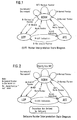
- Figure 1 is an illustration of the CCITT/ETSI state diagram while Figure 2 is a state diagram interpretation of the Bellcore requirements.
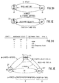
- the state diagram used in association with the present invention is presented in Figures 3A and 3E.
- the present invention uses an algorithm implemented in hardware so as to create an Alarm Indication Signal (AIS) and NO AIS state machine and a loss of pointer (LOP) and NO LOP state machine. These hardware implemented state machines are then mapped through an algorithm to produce a single equivalent state diagram as shown in Figures 3A and 3E.
- AIS Alarm Indication Signal
- LOP loss of pointer
- CCITT recognizes this condition and has added a path from AIS to LOP, however it does not have full coverage of the case described above.
- the present invention provides a system which overcomes the aforementioned difficulties.
- the present invention overcomes the above mentioned difficulties by treating an AIS condition as a subset of the LOP condition, exiting the AIS state when all ones does not exist for three frames, and defining an LOP as any sequence of pointers that do not meet the requirement to establish a valid pointer value within eight frames.
- LOP is active when AIS (all ones) is persistent.
- the associated software can easily be modified to latch or not latch the AIS alarm from the system perspective. If the requirements change with respect to latching AIS, extensive hardware changes can be avoided.
- the present invention is represented by a system for performing pointer interpretation according to Claim 1.
- the methodology of the present invention treats the Alarm Indication Signal (AIS) as a subset of the Loss of Pointer (LOP) state, thereby exiting AIS when all ones does not exist for three frames, and defining an LOP as any sequence of pointers that do not meet the requirement to establish a valid pointer value within 8-frames.
- AIS Alarm Indication Signal
- LOP Loss of Pointer
- the present invention remaps a first state machine defining a first type of AIS state and NO AIS state and a second state machine defining a first type of LOP state and NO LOP state into a third state machine defining a new (second) type of AIS state, a new (second) type of LOP state and a valid (in-range) pointer (NORM) state.
- AIS Alarm Indication Signal
- LOP Loss of Pointer
- a still further object of the present invention is to provide a method and system for SONET pointer interpretation in which the LOP state is defined as any sequence of pointers that do not meet the requirement to establish a valid pointer value within eight frames.
- Another object of the present invention is to provide a method and system for SONET pointer interpretation that can be applied to all synchronous transport modules as defined by Bellcore, ANSI, ETSI and CCITT, including but not limited to level 1 (STM-1), synchronous transport signal, level 1 (STS-1) and virtual tributary (VT and TU) pointer interpretation functions.
- STM-1 level 1
- STS-1 level 1
- VT and TU virtual tributary
- Figure 1 is a state diagram of the CCITT SONET pointer interpretation.
- Figure 2 is an interpretation of Bellcore document TR-TSY-000253 with respect to SONET pointer interpretation.
- Figure 3A is a SONET pointer interpretation state diagram according to the present invention.
- Figure 3B is a state diagram of a first type of AIS state to NO AIS state according to the present invention.
- Figure 3C is a state diagram of a first type of LOP state and NO LOP state according to the present invention.
- Figure 3D is a truth table for mapping the first type of AIS, NO AIS, LOP and NO LOP states into a new (second type) AIS state, a new (second type) LOP state and a NORM state.
- Figure 3E is a state diagram illustrating the AIS, LOP, and NORM states generated via the Figure 3D truth table, along with the transition events which correspond to the events and states shown in Figures 3A and 3B.
- Figure 4 is an overall block diagram of the transmit virtual tributary processing system implementing SONET pointer interpretation according to the present invention in which separate state machines are illustrated for AIS/NO AIS and LOP/NO LOP.
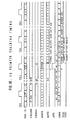
- FIG 5 is a timing diagram showing the transmitter serial bus interface (SBI) multi-frame synchronization waveforms for the system shown in Figure 4.
- SBI serial bus interface
- Figure 6 illustrates SBI multiframe counter timing information for the system shown in Figure 4.
- FIG 7 illustrates the synchronous payload envelope (SPE) counter sequence for the system shown in Figure 4.
- SPE synchronous payload envelope
- Figure 8 illustrates the timing associated with the transmitter pointer decrement counter.
- Figure 9 illustrates the timing associated with the transmitter pointer increment counter.
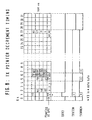
- Figure 10 illustrates the timing associated with transmitter pointer tracking.
- Figure 11A is a block diagram of the transmitter pointer interpretation logic circuitry corresponding to the pointer decode and pointer adjust control modules shown in Figure 4.
- Figure 11B illustrates the relationships of NEWPTR, OLDPTR and CURPTR, with respect to NPALL1, NDF3OF4, NDF1001, NDF0110 and how the INVALID state is enabled.
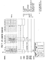
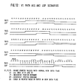
- Figure 12 illustrates timing diagrams for various AIS and LOP scenarios.
- the present invention relates to a system and method for robust, consistent implementation of the Synchronous Optical Network (SONET) pointer interpretation function.
- SONET Synchronous Optical Network
- the overall SONET specification is detailed in ANSI document TI.105-1988.
- Bellcore has detailed its implementation in Bellcore document TR-TSY-000253.
- CCITT has also presented its recommendation description for pointer interpretation in CCITT document G.783.
- the present invention approaches pointer interpretation from a different state diagram perspective which, is set forth in Figure 3A. It is believed that this state diagram implementation achieves several advantages over perceived shortcomings with both the CCITT pointer interpretation and the Bellcore interpretation.
- Bellcore TR-TSY-000253 states that the removal of the Alarm Indication Signal (AIS) is to be detected as a valid pointer observed for three consecutive frames.
- AIS Alarm Indication Signal
- LOP loss of pointer
- the CCITT document recognizes this occurrence and has added a path from AIS to LOP, however it does not have full coverage of the case described above.
- the present invention as illustrated in the state diagram of Figures 3A and 3E overcomes the above-mentioned difficulties by treating a first type of AIS state as a subset of a first type of LOP state, and exiting AIS when all ones does not exist for three consecutive frames.
- the present invention also defines the first type of LOP state as any sequence of pointers that do not meet the requirement to establish a valid pointer value within 8-frames.
- LOP is active when an AIS (all ones) is persistent.
- the software can easily be modified to maintain or discontinue the AIS alarm from a system perspective. If the requirements change with respect to latching AIS, expensive hardware changes are thereby avoided.
- the present invention takes the perspective that if the requirement to exit LOP does not exist, then the system should be in an LOP or AIS state.
- the present invention is error tolerant to one in eight errorred pointers due to bit errors.
- Table 1 illustrates the subtle differences between the AU-4 pointer defined by CCITT/ETSI in their G.783 recommendation and the Bellcore STS-3C pointer defined in their TR-TSY-000253 specification.
- the AU-4 pointer comprises three pointers of which one pointer (#1) carries the pointer value while #2 and #3 pointers are not used and carry fixed values as shown in Table 1.
- the STS-3C pointer comprises three concatenated STS-1 pointers, #1, #2, and #3 as shown in Table 1.
- Figure 1 illustrates the state diagram for the CCITT pointer definition
- Figure 2 illustrates a similar pointer definition based upon the Bellcore TR-TSY-000253 requirements.
- Table 2 presents the definition of pointer states for the CCITT definition, the Bellcore definition and that of the present invention.
- the state diagram corresponding to the transmit (TX) pointer interpretation module 41 ( Figure 11A) of the SONET pointer interpretation system 40 ( Figure 4) overcomes the incomplete Bellcore TR-TSY-000253 requirements and the CCITT/ETSI recommendation as noted above by treating a first type of Alarm Indication Signal (AIS) as a subset of a first type of Loss of Pointer state (LOP) and exiting AIS (transition from AIS to NO AIS state 21 ) when all ones does not exist for three consecutive frames, and defining the transition from the NO LOP state 23 to the LOP state 22 as any sequence of pointers that does not meet the requirement to establish a valid pointer value within eight frames.
- AIS Alarm Indication Signal
- LOP Loss of Pointer state
- Precise logic definitions are shown in Figures 3B and 3C, including the NDF bit pattern.
- NDF3OF4 means that a 3 of 4 bit match to pattern 1001 has been made by the pointer interpretation circuit 41 .
- the NDF1001 term simply means NDF active, which by definition is 1001. NDF inactive is thus 0110 (or any value other than 1001).
- Figure 3D The truth table shown in Figure 3D explains how the states shown in Figures 3B and 3C are transformed into the pointer interpretation state diagram shown in Figure 3E.
- Figure 3E corresponds to Figure 3A and makes clear that no Normal Pointer is the inverse (logic NOT) of transition events A AND B.
- the temporary AIS state shown in Figure 3D corresponds to the first three scenarios shown in Figure 12. Thus if AIS is true, LOP will become true if it is not already true.
- the present invention is error tolerant to one in eight errorred pointers due to bit errors as seen in the last LOP scenario of Figure 12.
- Figure 4 illustrates an overall block diagram of the transmitter VT processing module which implements VT1.5. SONET pointer interpretation.
- the input/output description of this overall block diagram is presented in Table 3, while the functions performed by this system are presented in Table 4.
- Block Inputs Block outputs: TXSBI ⁇ 15..0> TXVTO ⁇ 15..0> CKTCHI (256 KHz) TXWREN TXFSYNC (8 KHz) TXCH31 SBIERR S1DATA SPILL S2DATA SWTCHOVR TFIN TSTRST TXV1V3 TST6 TXINC TXDEC VTSIZE ⁇ 1..0> TXLOP TXPAIS TXV6V8 TXB1ERR TXB2ERR TXFEBE TXLABEL ⁇ 2..0> TXYELO TB125US RSTES
- the parallel data input (TXSBI ⁇ 15..0>) is retimed and output as TXVTO ⁇ 15..0>.
- the most significant eight bits of the retimed 16 bit input contains the VT SPE data and VI data. Details concerning the VI data are presented in applicant's U.S. Patent 5,027,349, entitled Imbedded Control Technique for Distributed Control Systems, which is hereby incorporated by reference.
- the least significant 8 bits contain the V-bit, I-bit, OFFSET address, and parity status of the channel during Channel-31, and the TFIN and MFS 2 bits during payload carrying channels. Only TXVT0 ⁇ 15..8> is sent to the TX partition multiplexer module.
- the TXVSYNC input 46 which comes from an active TX SBI input module is retimed and then used to synchronize the SBI multi-frame counter 48 to the frame boundary.
- the SBI multi-frame counter is a modulo 128 count counter.
- the MFS2 bit in the SBI parallel data (TXSBI ⁇ 15..0>) is extracted from channel-3 and filtered for a 011 pattern.
- the SBI multi-frame counter is synchronized on the multiframe boundary. See Figure 5 for timing details.
- the VT synchronization signals can be decoded from the multiframe counter 48 .
- TXVTEN is active only during SBI channels 2 through 27 which indicate the 104 byte synchronous payload envelope (SPE).
- SPE 104 byte synchronous payload envelope
- V1, V2,and V3 are active during channel-1 and indicate the location of the pointer within parallel data. See Figure 6 for timing details.
- the TFIN (transmit frame indicator) is extracted from the TFIN bit of the parallel SBI data and then filtered at filter module and 8-bit counter 50 .
- a filtered TFIN output goes to the two RX SBI output blocks for transmit multiframe synchronization.
- the filtering of TFIN prevents unwanted changes in the outgoing RX SBI multiframe synchronization due to parity errors and loss of frame events in the incoming TX SBI.
- To extract TFIN a 1100 pattern is detected in TXVT01 during channel 1 through 27.
- An 8-bit counter 50 regenerates TFIN for the RX SBI Output Blocks. If the 1100 pattern is not present at count 1 of the 8-bit counter two times consecutively, then the next occurence of the 1100 pattern resets the 8-bit counter to 2.
- a realignment of TFIN requires up to 24 frames (3ms).
- a VT SPE counter 52 (loadable modulo 104 down counter) is synchronized with the pointer and decrements when TXVTEN is active. To synchronize the counter, the value of the pointer is loaded in the SPE counter during TXV2. When the counter counts down to 0, the start of the SPE is indicated (V5). V5 is one of 4 VT overhead bytes in the SPE. The other 3 overhead bytes (V6, V7, and V8) are reserved and ignored. The next count (103) indicates a byte containing the 193rd DS1 bit, stuff opportunity bits, or stuff control bits. The remaining 96 counts contain 8-bit DS1 data. See Figure 7 for timing and implementation details.
- Pointer interpretation and tracking is performed by the decoding and comparison of three pointer values; the new pointer 54 (NEWPTR), the old pointer 56 (OLDPTR), and the current pointer 58 (CURPTR) (See Figure 11A).
- VT path AIS (TXPAIS) is derived from algorithms using only NEWPTR.
- Loss of pointer (TXLOP), LDPTR, and ADJEN are derived from algorithms using NEWPTR and OLDPTR.
- TXINC and TXDEC are derived from algorithms using NEWPTR and CURPTR. See Figures 3S - 3E, 8, 9, 10, 11A, 11B, and 12 for timing and implementation details.
- Truth table 3D describes the operation of the above-mentioned algorithms.
- the new V1 register is updated during TXV1 with the new V1 data and combined with TXVTO ⁇ 15..8> during TXV2 to form NEWPTR.
- the old V2 register is updated with the new V2 data which is used as the OLDPTR during the next VT super frame.
- VTSIZE ⁇ 1..0> is output from the new V1 register and sent to the RX VI Channel block for status reporting.
- TXLOP and TXPAIS are output from the pointer decoding block and sent to the RX VI Channel block for performance reporting.
- TXINC and TXDEC are output from the pointer adjustment control block and sent to the RX VI Channel block where they are accumulated for performance reporting.
- Stuff bit interpretation is performed on C1 and C2 (TXVTO ⁇ 15> and TXVTO ⁇ 14> respectively) which are identified during TXI2, TXI3, and TXI4.
- the result of the interpretation is output on S1DATA and S2DATA during TXI4.
- the data in the V5 byte is processed by calculating the BIP-2 errors and latching the FEBE and signal label into the V5 register, and filtering of YELLOW (See yellow filter 60 in Figure 4).
- the BIP-2 errors are output on TXB1ERR and TXB2ERR and sent to the RX BI Channel block where they are accumulated for performance reporting.
- TXFEBE, TXLABEL ⁇ 2..0> are also output to the RX VI Channel block for performance and status reporting.
- YELLOW must be active for ten consecutive VT super frames to set TXYELO or inactive for ten consecutive VT super frames to clear TXYELO.
- TXYELO is output to the RX VI Channel block for status reporting.
- the RX Channel block is clocked by CKRCHI which has no guaranteed phase relationship with CKTCHI. All outputs sent to the RX VI Channel block must be transferred properly to guarantee accurate accumulation and to avoid metastability problems.
- TXVIV3 is generated in the SBI Multiframe counter and output to the RX VI Channel block where an edge detection circuit is used to determine where TXINC and TXDEC are stable.
- TXV6V8 is generated in the VT SPE counter and output to the RX VI Channel block where an edge detection circuit is used to determine where TXB1ERR, TXB2RR, AND TXFEBE are stable.
- TXV1V3 and TXV6V8 must be glitch free outputs (registered).
- Bits 1 and 2 are used for error performance monitoring. A bit interleaved parity scheme is specified. Bit 1 is set such that parity of all odd-numbered bits (1, 3, 5, and 7) in all bytes of the previous VT SPE is even. Bit 2 is set similarly for the even-numbered bits.
- the calculation of the BIP-2 includes the VT POH bytes but excludes the VT Pointers. Even parity is generated by setting the BIP-2 bits so that there are an even number of ones in each of the 2-bit sequences including the BIP-2
- C1 and C2 Two sets (C1 and C2) of stuff control bits are used to control the two stuff opportunities, S1 and S2 respectively.
- C2 controls S2 in the same way.
- Majority vote shall be used to make the stuff decision in the desynchronizer so as to protect against single bit errors in the C-bits.
- New Data Flag (NDF) - The decoding is performed by accepting NDF set to '1001' if at least 3 bits match (See Figure 11A and 11B).
- the Bellcore's requirements in TR-TSY-000253 are inconsistent, incomplete and conflicting.
- the present invention as set forth in the state diagram shown in Figure 3A and 3E is believed to meet the requirements of this document while providing flexibility through which system software modifications can be made.
- the TX VT processing system shown in Figure 4 achieves the state diagram implementation shown in Figures 3B and 3C which provides a more stable hardware implementation and meets the intent of both the CCITT and Bellcore requirements. In so doing, it specifically exits AIS when all ones does not exist for three frames and defines an LOP as any sequence of pointers that do not meet the requirements to establish a valid pointer value within eight frames.
- the present invention can be applied to various pointer protocols, including synchronous transport module level 1 (STM-1), synchronous transport signal level 1 (STS-1), virtual tributary (VT) CCITT tributary unit (TU) and administrative unit (AU) pointer interpretation functions.
- STM-1 synchronous transport module level 1
- STS-1 synchronous transport signal level 1
- VT virtual tributary CCITT tributary unit
- AU administrative unit
- Applications for the present invention therefore include STS-1 pointer interpretation, STS-3c pointer interpretation, VT pointer interpretation (VT1.5, VT2, VT3, and VT6), STM-1 pointer interpretation (CCITT AU4 PAYLOAD), and TU (tributary unit) pointer interpretation (CCITT payloads which include TU32, TU21, TU11, TU12, TU22 and TU32).
Landscapes
- Engineering & Computer Science (AREA)
- Computer Hardware Design (AREA)
- Computer Networks & Wireless Communication (AREA)
- Signal Processing (AREA)
- Time-Division Multiplex Systems (AREA)
- Chemical And Physical Treatments For Wood And The Like (AREA)
- Medicines Containing Antibodies Or Antigens For Use As Internal Diagnostic Agents (AREA)
- Medicines That Contain Protein Lipid Enzymes And Other Medicines (AREA)
- Alarm Systems (AREA)
Claims (1)
- System (40) zur Durchführung einer Zeigerinterpretation, bei dem der Zeiger in einem von drei Zuständen interpretiert werden kann, nämlich normal NORM, Verlust des Zeigers LOP eines zweiten Typs oder Alarmmeldesignal AIS eines zweiten Typs, wobei der Zeiger ein Markierungszeichen für neue Daten NDF enthält, das eine Vielzahl von Bits hat, so daß NDF aktiv ist, wenn sein Bitmuster in einer ersten Konfiguration ist, und wobei NDF inaktiv ist, wenn sein Bitmuster in einer zweiten Konfiguration ist, wobei das System folgendes umfaßt:A) Mittel (41) zum Empfang eines Zeigerwertes;B) Mittel (54, 56) zur Speicherung von mindestens einem Teil der beiden zuletzt empfangenen Zeigerwerte;C) Mittel (20) zur Eingabe eines ersten Typs des AIS-Zustands, wenn drei aufeinanderfolgende Zeiger empfangen werden, wobei sich jeder Zeiger in einem ganz aus Einsen bestehenden Zustand befindet;D) Mittel (21) zur Eingabe eines NO-AIS-Zustands des ersten Typs, wenn1) ein gültiger Zeiger empfangen wird und das NDF ein Bitmuster in der ersten Konfiguration hat oder2) sich jeder der drei zuletzt empfangenen Zeiger nicht in einem ganz aus Einsen bestehenden Zustand befindet;E) Mittel, die mit den Speichermitteln (54, 56) verbunden sind, um drei aufeinanderfolgende Zeigerwerte, die den beiden in den Speichermitteln (54, 56) gespeicherten Werten und dem am Empfangsmittel (41) empfangenen Wert entsprechen, zu vergleichen, um entweder ein 2MATCH-Ja-Signal zu erzeugen, wenn die drei Zeigerwerte übereinstimmen und nicht gültig sind, oder um andernfalls ein
 F) Mittel, die mit dem Vergleichsmittel verbunden sind, um einen ersten Typ des LOP-Zustands einzugeben, wenn achtmal hintereinander entweder "NDF nicht in der zweiten Konfiguration" oder die Erzeugung des 2MATCH-Nein-Signals (
 G) Mittel zur Eingabe eines NO-LOP-Zustands des ersten Typs, wenn1) ein gültiger Zeiger und NDF in der ersten Konfiguration und AIS des ersten Typs festgestellt werden oder2) das 2MATCH-Ja-Signal erzeugt wird und drei NDFs in der zweiten Konfiguration festgestellt worden sind, undH) Mittel, die mit dem AIS-Zustand des ersten Typs, dem NO-AIS-Zustand des ersten Typs, dem LOP-Zustand des ersten Typs und dem NO-LOP-Zustand des ersten Typs verbunden sind, um die Zustände in den AIS-Zustand des zweiten Typs, den LOP-Zustand des zweiten Typs und den NORM-Zustand umzusetzen.
Applications Claiming Priority (2)
| Application Number | Priority Date | Filing Date | Title |
|---|---|---|---|
| US07/771,038 US5210762A (en) | 1991-10-02 | 1991-10-02 | Sonet pointer interpretation system and method |
| US771038 | 1991-10-02 |
Publications (2)
| Publication Number | Publication Date |
|---|---|
| EP0539758A1 EP0539758A1 (de) | 1993-05-05 |
| EP0539758B1 true EP0539758B1 (de) | 1997-02-19 |
Family
ID=25090497
Family Applications (1)
| Application Number | Title | Priority Date | Filing Date |
|---|---|---|---|
| EP92116908A Expired - Lifetime EP0539758B1 (de) | 1991-10-02 | 1992-10-02 | Anordnung zur Auswertung von Sonetanzeigern |
Country Status (6)
| Country | Link |
|---|---|
| US (1) | US5210762A (de) |
| EP (1) | EP0539758B1 (de) |
| AT (1) | ATE149067T1 (de) |
| CA (1) | CA2079631A1 (de) |
| DE (1) | DE69217533T2 (de) |
| ES (1) | ES2100995T3 (de) |
Families Citing this family (18)
| Publication number | Priority date | Publication date | Assignee | Title |
|---|---|---|---|---|
| CA2076238C (en) * | 1991-08-21 | 1997-12-30 | Yoshihide Kuroda | Sonet transmission signal processing method and sonet transmission signal processing apparatus |
| US5706299A (en) * | 1992-05-21 | 1998-01-06 | Alcatel Network Systems, Inc. | Sonet tributary ambiguity resolution for elastic store control |
| FI91697C (fi) * | 1992-07-01 | 1994-07-25 | Nokia Telecommunications Oy | Menetelmä synkronisessa digitaalisessa tietoliikennejärjestelmässä käytettävän signaalin vastaanottamiseksi |
| FI91698C (fi) * | 1992-07-01 | 1994-07-25 | Nokia Telecommunications Oy | Menetelmä synkronisessa digitaalisessa tietoliikennejärjestelmässä käytettävän signaalin vastaanottamiseksi |
| FI91692C (fi) * | 1992-07-24 | 1994-07-25 | Nokia Telecommunications Oy | Menetelmä synkronisessa digitaalisessa tietoliikennejärjestelmässä käytettävän signaalin vastaanottamiseksi |
| JP2502263B2 (ja) * | 1993-06-18 | 1996-05-29 | 日本電気株式会社 | エラ―検出方式 |
| FI94813C (fi) * | 1993-11-12 | 1995-10-25 | Nokia Telecommunications Oy | Menetelmä synkronisessa digitaalisessa tietoliikennejärjestelmässä käytettävän signaalin vastaanottamiseksi |
| IT1265424B1 (it) * | 1993-12-22 | 1996-11-22 | Alcatel Italia | Metodo e disposizione ciruitale di realizzazione della funzione di hpa negli apparati sdh |
| IT1275266B (it) * | 1995-05-29 | 1997-08-05 | Alcatel Italia | Metodo e circuiti per la interpretazione del puntatore in dispositivi della gerarchia numerica sincrona sdh |
| US5535219A (en) * | 1995-06-14 | 1996-07-09 | National Semiconductor Corp. | Sonet/SDH pointer calculation circuit |
| US5841762A (en) * | 1996-03-29 | 1998-11-24 | British Telecommunications Public Limited Company | Monitoring a synchronous digital hierarchy transmission path |
| IL133504A (en) * | 1999-12-14 | 2004-02-08 | Eci Telecom Ltd | Handling an alarm situation in a telecommunication system |
| US6981228B1 (en) * | 2000-09-29 | 2005-12-27 | Sbc Technology Resources, Inc. | Interactive topology graphs for visualization and characterization of SONET consumption patterns |
| US7362759B2 (en) * | 2001-05-21 | 2008-04-22 | Intel Corporation | Method and apparatus for encoding information |
| US7158517B2 (en) * | 2001-05-21 | 2007-01-02 | Intel Corporation | Method and apparatus for frame-based protocol processing |
| US7212599B2 (en) * | 2002-01-25 | 2007-05-01 | Applied Micro Circuits Corporation | Jitter and wander reduction apparatus |
| US7305014B2 (en) * | 2003-04-22 | 2007-12-04 | David Kirk | Synchronous system bus |
| US20060067314A1 (en) * | 2004-09-29 | 2006-03-30 | Michael Ho | Overhead processing and generation techniques |
Family Cites Families (2)
| Publication number | Priority date | Publication date | Assignee | Title |
|---|---|---|---|---|
| US4967405A (en) * | 1988-12-09 | 1990-10-30 | Transwitch Corporation | System for cross-connecting high speed digital SONET signals |
| US4964095A (en) * | 1989-05-12 | 1990-10-16 | Alcatel Na, Inc. | Data communication bypass apparatus and method |
-
1991
- 1991-10-02 US US07/771,038 patent/US5210762A/en not_active Expired - Lifetime
-
1992
- 1992-10-01 CA CA002079631A patent/CA2079631A1/en not_active Abandoned
- 1992-10-02 ES ES92116908T patent/ES2100995T3/es not_active Expired - Lifetime
- 1992-10-02 EP EP92116908A patent/EP0539758B1/de not_active Expired - Lifetime
- 1992-10-02 AT AT92116908T patent/ATE149067T1/de not_active IP Right Cessation
- 1992-10-02 DE DE69217533T patent/DE69217533T2/de not_active Expired - Lifetime
Also Published As
| Publication number | Publication date |
|---|---|
| EP0539758A1 (de) | 1993-05-05 |
| ATE149067T1 (de) | 1997-03-15 |
| US5210762A (en) | 1993-05-11 |
| DE69217533T2 (de) | 1997-07-03 |
| CA2079631A1 (en) | 1993-04-03 |
| ES2100995T3 (es) | 1997-07-01 |
| DE69217533D1 (de) | 1997-03-27 |
Similar Documents
| Publication | Publication Date | Title |
|---|---|---|
| US5210762A (en) | Sonet pointer interpretation system and method | |
| US5065396A (en) | Inverse multiplexer and demultiplexer techniques | |
| AU620744B2 (en) | Method for transmitting a digital broadband signal in a tributary unit concatenation via a network of a synchronous digital multiplex hierarchy | |
| US6493847B1 (en) | Sonet B2 parity byte calculation method and apparatus | |
| EP0969617B1 (de) | Verfahren und Vorrichtung zur Steuerung von virtuell verketteten Kanälen | |
| US5751720A (en) | Pointer processor and pointer processing scheme for SDH/SONET transmission system | |
| JPH0738545A (ja) | 平滑出力クロック信号抽出方法 | |
| US5539750A (en) | Method for receiving a signal used in a synchronous digital telecommunication system | |
| EP0525770B1 (de) | Vorrichtung und Verfahren zur Erneuerung von AU-4 und TU-3 Zeigern der digitalen synchronen Hierarchien | |
| WO2003032540A2 (en) | Method and apparatus for digital data synchronization | |
| US5768282A (en) | Node provided with facility for checking establishment of synchronization | |
| EP0728389B1 (de) | Verfahren zum empfang eines signals in einem synchronen digitalen telekommunikationssystem | |
| EP0648394B1 (de) | Verfahren zum empfangen eines signals in einem synchronen digitalen übertragungssystem | |
| KR100271311B1 (ko) | 광가입자 전송장치에서의 관리단위신호에 대한 관리단위 포인터및 계위단위 포인터 처리장치 | |
| US7508830B1 (en) | Method and apparatus differential delay compensation processing of virtually concatenated data | |
| JP3271444B2 (ja) | Bip−2演算回路およびbip−2チェック回路 | |
| Henderson | Fundamentals of SONET/SDH | |
| KR100201330B1 (ko) | 동기식 다중화장치에서 tu포인터 버퍼 리셋에 따른v5클럭 보상회로 | |
| KR100201332B1 (ko) | 동기식 다중화장치에서 vc1 자국 루프백회로 | |
| KR0153688B1 (ko) | 동기식 전송장치에 있어서 dram을 이용한 tu신호 정렬장치 | |
| KR100201328B1 (ko) | 동기식 다중화장치의 ds1 매핑 회로 | |
| WO1994003000A1 (en) | Method for receiving a signal used in a synchronous digital telecommunication system | |
| KR100252501B1 (ko) | 동기식 다중화장치에서 | |
| Autry | Minimization of jitter in SDH/SONET networks via an all-digital desynchronizer | |
| Autry | 3.4 SONET and SDH |
Legal Events
| Date | Code | Title | Description |
|---|---|---|---|
| PUAI | Public reference made under article 153(3) epc to a published international application that has entered the european phase |
Free format text: ORIGINAL CODE: 0009012 |
|
| AK | Designated contracting states |
Kind code of ref document: A1 Designated state(s): AT BE CH DE ES FR GB IT LI NL SE |
|
| 17P | Request for examination filed |
Effective date: 19930716 |
|
| 17Q | First examination report despatched |
Effective date: 19951023 |
|
| GRAG | Despatch of communication of intention to grant |
Free format text: ORIGINAL CODE: EPIDOS AGRA |
|
| GRAH | Despatch of communication of intention to grant a patent |
Free format text: ORIGINAL CODE: EPIDOS IGRA |
|
| GRAH | Despatch of communication of intention to grant a patent |
Free format text: ORIGINAL CODE: EPIDOS IGRA |
|
| GRAA | (expected) grant |
Free format text: ORIGINAL CODE: 0009210 |
|
| AK | Designated contracting states |
Kind code of ref document: B1 Designated state(s): AT BE CH DE ES FR GB IT LI NL SE |
|
| REF | Corresponds to: |
Ref document number: 149067 Country of ref document: AT Date of ref document: 19970315 Kind code of ref document: T |
|
| REG | Reference to a national code |
Ref country code: CH Ref legal event code: EP Ref country code: CH Ref legal event code: NV Representative=s name: JUERG ULRICH C/O ALCATEL STR AG |
|
| REF | Corresponds to: |
Ref document number: 69217533 Country of ref document: DE Date of ref document: 19970327 |
|
| ITF | It: translation for a ep patent filed | ||
| ET | Fr: translation filed | ||
| REG | Reference to a national code |
Ref country code: ES Ref legal event code: FG2A Ref document number: 2100995 Country of ref document: ES Kind code of ref document: T3 |
|
| PLBE | No opposition filed within time limit |
Free format text: ORIGINAL CODE: 0009261 |
|
| 26N | No opposition filed | ||
| PGFP | Annual fee paid to national office [announced via postgrant information from national office to epo] |
Ref country code: NL Payment date: 19990923 Year of fee payment: 8 |
|
| PGFP | Annual fee paid to national office [announced via postgrant information from national office to epo] |
Ref country code: BE Payment date: 19990929 Year of fee payment: 8 |
|
| PG25 | Lapsed in a contracting state [announced via postgrant information from national office to epo] |
Ref country code: BE Free format text: LAPSE BECAUSE OF NON-PAYMENT OF DUE FEES Effective date: 20001031 |
|
| BERE | Be: lapsed |
Owner name: ALCATEL N.V. Effective date: 20001031 |
|
| PG25 | Lapsed in a contracting state [announced via postgrant information from national office to epo] |
Ref country code: NL Free format text: LAPSE BECAUSE OF NON-PAYMENT OF DUE FEES Effective date: 20010501 |
|
| NLV4 | Nl: lapsed or anulled due to non-payment of the annual fee |
Effective date: 20010501 |
|
| REG | Reference to a national code |
Ref country code: GB Ref legal event code: IF02 |
|
| PGFP | Annual fee paid to national office [announced via postgrant information from national office to epo] |
Ref country code: CH Payment date: 20020918 Year of fee payment: 11 |
|
| PGFP | Annual fee paid to national office [announced via postgrant information from national office to epo] |
Ref country code: SE Payment date: 20021002 Year of fee payment: 11 |
|
| PGFP | Annual fee paid to national office [announced via postgrant information from national office to epo] |
Ref country code: AT Payment date: 20021003 Year of fee payment: 11 |
|
| PGFP | Annual fee paid to national office [announced via postgrant information from national office to epo] |
Ref country code: ES Payment date: 20021017 Year of fee payment: 11 |
|
| PG25 | Lapsed in a contracting state [announced via postgrant information from national office to epo] |
Ref country code: AT Free format text: LAPSE BECAUSE OF NON-PAYMENT OF DUE FEES Effective date: 20031002 |
|
| PG25 | Lapsed in a contracting state [announced via postgrant information from national office to epo] |
Ref country code: ES Free format text: LAPSE BECAUSE OF NON-PAYMENT OF DUE FEES Effective date: 20031003 Ref country code: SE Free format text: LAPSE BECAUSE OF NON-PAYMENT OF DUE FEES Effective date: 20031003 |
|
| PG25 | Lapsed in a contracting state [announced via postgrant information from national office to epo] |
Ref country code: CH Free format text: LAPSE BECAUSE OF NON-PAYMENT OF DUE FEES Effective date: 20031031 Ref country code: LI Free format text: LAPSE BECAUSE OF NON-PAYMENT OF DUE FEES Effective date: 20031031 |
|
| EUG | Se: european patent has lapsed | ||
| REG | Reference to a national code |
Ref country code: CH Ref legal event code: PL |
|
| REG | Reference to a national code |
Ref country code: ES Ref legal event code: FD2A Effective date: 20031003 |
|
| PGFP | Annual fee paid to national office [announced via postgrant information from national office to epo] |
Ref country code: DE Payment date: 20091026 Year of fee payment: 18 |
|
| PGFP | Annual fee paid to national office [announced via postgrant information from national office to epo] |
Ref country code: GB Payment date: 20091022 Year of fee payment: 18 Ref country code: IT Payment date: 20091028 Year of fee payment: 18 Ref country code: FR Payment date: 20091110 Year of fee payment: 18 |
|
| GBPC | Gb: european patent ceased through non-payment of renewal fee |
Effective date: 20101002 |
|
| PG25 | Lapsed in a contracting state [announced via postgrant information from national office to epo] |
Ref country code: FR Free format text: LAPSE BECAUSE OF NON-PAYMENT OF DUE FEES Effective date: 20101102 |
|
| REG | Reference to a national code |
Ref country code: FR Ref legal event code: ST Effective date: 20110630 |
|
| REG | Reference to a national code |
Ref country code: DE Ref legal event code: R119 Ref document number: 69217533 Country of ref document: DE Effective date: 20110502 |
|
| PG25 | Lapsed in a contracting state [announced via postgrant information from national office to epo] |
Ref country code: GB Free format text: LAPSE BECAUSE OF NON-PAYMENT OF DUE FEES Effective date: 20101002 |
|
| PG25 | Lapsed in a contracting state [announced via postgrant information from national office to epo] |
Ref country code: IT Free format text: LAPSE BECAUSE OF NON-PAYMENT OF DUE FEES Effective date: 20101002 |
|
| PG25 | Lapsed in a contracting state [announced via postgrant information from national office to epo] |
Ref country code: DE Free format text: LAPSE BECAUSE OF NON-PAYMENT OF DUE FEES Effective date: 20110502 |