EP0533589A1 - A semiconductor device - Google Patents
A semiconductor device Download PDFInfo
- Publication number
- EP0533589A1 EP0533589A1 EP92402587A EP92402587A EP0533589A1 EP 0533589 A1 EP0533589 A1 EP 0533589A1 EP 92402587 A EP92402587 A EP 92402587A EP 92402587 A EP92402587 A EP 92402587A EP 0533589 A1 EP0533589 A1 EP 0533589A1
- Authority
- EP
- European Patent Office
- Prior art keywords
- signal
- receiving
- formation surface
- bonding pad
- solely
- Prior art date
- Legal status (The legal status is an assumption and is not a legal conclusion. Google has not performed a legal analysis and makes no representation as to the accuracy of the status listed.)
- Granted
Links
Images


Classifications
-
- H—ELECTRICITY
- H01—ELECTRIC ELEMENTS
- H01L—SEMICONDUCTOR DEVICES NOT COVERED BY CLASS H10
- H01L24/00—Arrangements for connecting or disconnecting semiconductor or solid-state bodies; Methods or apparatus related thereto
- H01L24/01—Means for bonding being attached to, or being formed on, the surface to be connected, e.g. chip-to-package, die-attach, "first-level" interconnects; Manufacturing methods related thereto
- H01L24/02—Bonding areas ; Manufacturing methods related thereto
- H01L24/04—Structure, shape, material or disposition of the bonding areas prior to the connecting process
- H01L24/06—Structure, shape, material or disposition of the bonding areas prior to the connecting process of a plurality of bonding areas
-
- H—ELECTRICITY
- H01—ELECTRIC ELEMENTS
- H01L—SEMICONDUCTOR DEVICES NOT COVERED BY CLASS H10
- H01L23/00—Details of semiconductor or other solid state devices
- H01L23/48—Arrangements for conducting electric current to or from the solid state body in operation, e.g. leads, terminal arrangements ; Selection of materials therefor
- H01L23/488—Arrangements for conducting electric current to or from the solid state body in operation, e.g. leads, terminal arrangements ; Selection of materials therefor consisting of soldered or bonded constructions
- H01L23/495—Lead-frames or other flat leads
- H01L23/49503—Lead-frames or other flat leads characterised by the die pad
- H01L23/4951—Chip-on-leads or leads-on-chip techniques, i.e. inner lead fingers being used as die pad
-
- H—ELECTRICITY
- H01—ELECTRIC ELEMENTS
- H01L—SEMICONDUCTOR DEVICES NOT COVERED BY CLASS H10
- H01L23/00—Details of semiconductor or other solid state devices
- H01L23/48—Arrangements for conducting electric current to or from the solid state body in operation, e.g. leads, terminal arrangements ; Selection of materials therefor
- H01L23/50—Arrangements for conducting electric current to or from the solid state body in operation, e.g. leads, terminal arrangements ; Selection of materials therefor for integrated circuit devices, e.g. power bus, number of leads
-
- H—ELECTRICITY
- H01—ELECTRIC ELEMENTS
- H01L—SEMICONDUCTOR DEVICES NOT COVERED BY CLASS H10
- H01L24/00—Arrangements for connecting or disconnecting semiconductor or solid-state bodies; Methods or apparatus related thereto
- H01L24/01—Means for bonding being attached to, or being formed on, the surface to be connected, e.g. chip-to-package, die-attach, "first-level" interconnects; Manufacturing methods related thereto
- H01L24/42—Wire connectors; Manufacturing methods related thereto
- H01L24/47—Structure, shape, material or disposition of the wire connectors after the connecting process
- H01L24/49—Structure, shape, material or disposition of the wire connectors after the connecting process of a plurality of wire connectors
-
- H—ELECTRICITY
- H01—ELECTRIC ELEMENTS
- H01L—SEMICONDUCTOR DEVICES NOT COVERED BY CLASS H10
- H01L2224/00—Indexing scheme for arrangements for connecting or disconnecting semiconductor or solid-state bodies and methods related thereto as covered by H01L24/00
- H01L2224/01—Means for bonding being attached to, or being formed on, the surface to be connected, e.g. chip-to-package, die-attach, "first-level" interconnects; Manufacturing methods related thereto
- H01L2224/02—Bonding areas; Manufacturing methods related thereto
- H01L2224/04—Structure, shape, material or disposition of the bonding areas prior to the connecting process
- H01L2224/04042—Bonding areas specifically adapted for wire connectors, e.g. wirebond pads
-
- H—ELECTRICITY
- H01—ELECTRIC ELEMENTS
- H01L—SEMICONDUCTOR DEVICES NOT COVERED BY CLASS H10
- H01L2224/00—Indexing scheme for arrangements for connecting or disconnecting semiconductor or solid-state bodies and methods related thereto as covered by H01L24/00
- H01L2224/01—Means for bonding being attached to, or being formed on, the surface to be connected, e.g. chip-to-package, die-attach, "first-level" interconnects; Manufacturing methods related thereto
- H01L2224/02—Bonding areas; Manufacturing methods related thereto
- H01L2224/04—Structure, shape, material or disposition of the bonding areas prior to the connecting process
- H01L2224/05—Structure, shape, material or disposition of the bonding areas prior to the connecting process of an individual bonding area
- H01L2224/0554—External layer
- H01L2224/0555—Shape
- H01L2224/05552—Shape in top view
- H01L2224/05554—Shape in top view being square
-
- H—ELECTRICITY
- H01—ELECTRIC ELEMENTS
- H01L—SEMICONDUCTOR DEVICES NOT COVERED BY CLASS H10
- H01L2224/00—Indexing scheme for arrangements for connecting or disconnecting semiconductor or solid-state bodies and methods related thereto as covered by H01L24/00
- H01L2224/01—Means for bonding being attached to, or being formed on, the surface to be connected, e.g. chip-to-package, die-attach, "first-level" interconnects; Manufacturing methods related thereto
- H01L2224/02—Bonding areas; Manufacturing methods related thereto
- H01L2224/04—Structure, shape, material or disposition of the bonding areas prior to the connecting process
- H01L2224/05—Structure, shape, material or disposition of the bonding areas prior to the connecting process of an individual bonding area
- H01L2224/0554—External layer
- H01L2224/05599—Material
- H01L2224/056—Material with a principal constituent of the material being a metal or a metalloid, e.g. boron [B], silicon [Si], germanium [Ge], arsenic [As], antimony [Sb], tellurium [Te] and polonium [Po], and alloys thereof
- H01L2224/05617—Material with a principal constituent of the material being a metal or a metalloid, e.g. boron [B], silicon [Si], germanium [Ge], arsenic [As], antimony [Sb], tellurium [Te] and polonium [Po], and alloys thereof the principal constituent melting at a temperature of greater than or equal to 400°C and less than 950°C
- H01L2224/05624—Aluminium [Al] as principal constituent
-
- H—ELECTRICITY
- H01—ELECTRIC ELEMENTS
- H01L—SEMICONDUCTOR DEVICES NOT COVERED BY CLASS H10
- H01L2224/00—Indexing scheme for arrangements for connecting or disconnecting semiconductor or solid-state bodies and methods related thereto as covered by H01L24/00
- H01L2224/01—Means for bonding being attached to, or being formed on, the surface to be connected, e.g. chip-to-package, die-attach, "first-level" interconnects; Manufacturing methods related thereto
- H01L2224/02—Bonding areas; Manufacturing methods related thereto
- H01L2224/04—Structure, shape, material or disposition of the bonding areas prior to the connecting process
- H01L2224/06—Structure, shape, material or disposition of the bonding areas prior to the connecting process of a plurality of bonding areas
- H01L2224/061—Disposition
- H01L2224/0612—Layout
- H01L2224/0613—Square or rectangular array
- H01L2224/06134—Square or rectangular array covering only portions of the surface to be connected
- H01L2224/06136—Covering only the central area of the surface to be connected, i.e. central arrangements
-
- H—ELECTRICITY
- H01—ELECTRIC ELEMENTS
- H01L—SEMICONDUCTOR DEVICES NOT COVERED BY CLASS H10
- H01L2224/00—Indexing scheme for arrangements for connecting or disconnecting semiconductor or solid-state bodies and methods related thereto as covered by H01L24/00
- H01L2224/01—Means for bonding being attached to, or being formed on, the surface to be connected, e.g. chip-to-package, die-attach, "first-level" interconnects; Manufacturing methods related thereto
- H01L2224/26—Layer connectors, e.g. plate connectors, solder or adhesive layers; Manufacturing methods related thereto
- H01L2224/31—Structure, shape, material or disposition of the layer connectors after the connecting process
- H01L2224/32—Structure, shape, material or disposition of the layer connectors after the connecting process of an individual layer connector
- H01L2224/321—Disposition
- H01L2224/32151—Disposition the layer connector connecting between a semiconductor or solid-state body and an item not being a semiconductor or solid-state body, e.g. chip-to-substrate, chip-to-passive
- H01L2224/32221—Disposition the layer connector connecting between a semiconductor or solid-state body and an item not being a semiconductor or solid-state body, e.g. chip-to-substrate, chip-to-passive the body and the item being stacked
- H01L2224/32245—Disposition the layer connector connecting between a semiconductor or solid-state body and an item not being a semiconductor or solid-state body, e.g. chip-to-substrate, chip-to-passive the body and the item being stacked the item being metallic
-
- H—ELECTRICITY
- H01—ELECTRIC ELEMENTS
- H01L—SEMICONDUCTOR DEVICES NOT COVERED BY CLASS H10
- H01L2224/00—Indexing scheme for arrangements for connecting or disconnecting semiconductor or solid-state bodies and methods related thereto as covered by H01L24/00
- H01L2224/01—Means for bonding being attached to, or being formed on, the surface to be connected, e.g. chip-to-package, die-attach, "first-level" interconnects; Manufacturing methods related thereto
- H01L2224/42—Wire connectors; Manufacturing methods related thereto
- H01L2224/44—Structure, shape, material or disposition of the wire connectors prior to the connecting process
- H01L2224/45—Structure, shape, material or disposition of the wire connectors prior to the connecting process of an individual wire connector
- H01L2224/45001—Core members of the connector
- H01L2224/45099—Material
- H01L2224/451—Material with a principal constituent of the material being a metal or a metalloid, e.g. boron (B), silicon (Si), germanium (Ge), arsenic (As), antimony (Sb), tellurium (Te) and polonium (Po), and alloys thereof
- H01L2224/45138—Material with a principal constituent of the material being a metal or a metalloid, e.g. boron (B), silicon (Si), germanium (Ge), arsenic (As), antimony (Sb), tellurium (Te) and polonium (Po), and alloys thereof the principal constituent melting at a temperature of greater than or equal to 950°C and less than 1550°C
- H01L2224/45144—Gold (Au) as principal constituent
-
- H—ELECTRICITY
- H01—ELECTRIC ELEMENTS
- H01L—SEMICONDUCTOR DEVICES NOT COVERED BY CLASS H10
- H01L2224/00—Indexing scheme for arrangements for connecting or disconnecting semiconductor or solid-state bodies and methods related thereto as covered by H01L24/00
- H01L2224/01—Means for bonding being attached to, or being formed on, the surface to be connected, e.g. chip-to-package, die-attach, "first-level" interconnects; Manufacturing methods related thereto
- H01L2224/42—Wire connectors; Manufacturing methods related thereto
- H01L2224/47—Structure, shape, material or disposition of the wire connectors after the connecting process
- H01L2224/48—Structure, shape, material or disposition of the wire connectors after the connecting process of an individual wire connector
- H01L2224/4805—Shape
- H01L2224/4809—Loop shape
- H01L2224/48091—Arched
-
- H—ELECTRICITY
- H01—ELECTRIC ELEMENTS
- H01L—SEMICONDUCTOR DEVICES NOT COVERED BY CLASS H10
- H01L2224/00—Indexing scheme for arrangements for connecting or disconnecting semiconductor or solid-state bodies and methods related thereto as covered by H01L24/00
- H01L2224/01—Means for bonding being attached to, or being formed on, the surface to be connected, e.g. chip-to-package, die-attach, "first-level" interconnects; Manufacturing methods related thereto
- H01L2224/42—Wire connectors; Manufacturing methods related thereto
- H01L2224/47—Structure, shape, material or disposition of the wire connectors after the connecting process
- H01L2224/48—Structure, shape, material or disposition of the wire connectors after the connecting process of an individual wire connector
- H01L2224/481—Disposition
- H01L2224/4813—Connecting within a semiconductor or solid-state body, i.e. fly wire, bridge wire
-
- H—ELECTRICITY
- H01—ELECTRIC ELEMENTS
- H01L—SEMICONDUCTOR DEVICES NOT COVERED BY CLASS H10
- H01L2224/00—Indexing scheme for arrangements for connecting or disconnecting semiconductor or solid-state bodies and methods related thereto as covered by H01L24/00
- H01L2224/01—Means for bonding being attached to, or being formed on, the surface to be connected, e.g. chip-to-package, die-attach, "first-level" interconnects; Manufacturing methods related thereto
- H01L2224/42—Wire connectors; Manufacturing methods related thereto
- H01L2224/47—Structure, shape, material or disposition of the wire connectors after the connecting process
- H01L2224/48—Structure, shape, material or disposition of the wire connectors after the connecting process of an individual wire connector
- H01L2224/481—Disposition
- H01L2224/48151—Connecting between a semiconductor or solid-state body and an item not being a semiconductor or solid-state body, e.g. chip-to-substrate, chip-to-passive
- H01L2224/48221—Connecting between a semiconductor or solid-state body and an item not being a semiconductor or solid-state body, e.g. chip-to-substrate, chip-to-passive the body and the item being stacked
- H01L2224/48245—Connecting between a semiconductor or solid-state body and an item not being a semiconductor or solid-state body, e.g. chip-to-substrate, chip-to-passive the body and the item being stacked the item being metallic
- H01L2224/48247—Connecting between a semiconductor or solid-state body and an item not being a semiconductor or solid-state body, e.g. chip-to-substrate, chip-to-passive the body and the item being stacked the item being metallic connecting the wire to a bond pad of the item
-
- H—ELECTRICITY
- H01—ELECTRIC ELEMENTS
- H01L—SEMICONDUCTOR DEVICES NOT COVERED BY CLASS H10
- H01L2224/00—Indexing scheme for arrangements for connecting or disconnecting semiconductor or solid-state bodies and methods related thereto as covered by H01L24/00
- H01L2224/01—Means for bonding being attached to, or being formed on, the surface to be connected, e.g. chip-to-package, die-attach, "first-level" interconnects; Manufacturing methods related thereto
- H01L2224/42—Wire connectors; Manufacturing methods related thereto
- H01L2224/47—Structure, shape, material or disposition of the wire connectors after the connecting process
- H01L2224/48—Structure, shape, material or disposition of the wire connectors after the connecting process of an individual wire connector
- H01L2224/481—Disposition
- H01L2224/48151—Connecting between a semiconductor or solid-state body and an item not being a semiconductor or solid-state body, e.g. chip-to-substrate, chip-to-passive
- H01L2224/48221—Connecting between a semiconductor or solid-state body and an item not being a semiconductor or solid-state body, e.g. chip-to-substrate, chip-to-passive the body and the item being stacked
- H01L2224/48245—Connecting between a semiconductor or solid-state body and an item not being a semiconductor or solid-state body, e.g. chip-to-substrate, chip-to-passive the body and the item being stacked the item being metallic
- H01L2224/4826—Connecting between the body and an opposite side of the item with respect to the body
-
- H—ELECTRICITY
- H01—ELECTRIC ELEMENTS
- H01L—SEMICONDUCTOR DEVICES NOT COVERED BY CLASS H10
- H01L2224/00—Indexing scheme for arrangements for connecting or disconnecting semiconductor or solid-state bodies and methods related thereto as covered by H01L24/00
- H01L2224/01—Means for bonding being attached to, or being formed on, the surface to be connected, e.g. chip-to-package, die-attach, "first-level" interconnects; Manufacturing methods related thereto
- H01L2224/42—Wire connectors; Manufacturing methods related thereto
- H01L2224/47—Structure, shape, material or disposition of the wire connectors after the connecting process
- H01L2224/48—Structure, shape, material or disposition of the wire connectors after the connecting process of an individual wire connector
- H01L2224/485—Material
- H01L2224/48505—Material at the bonding interface
- H01L2224/48599—Principal constituent of the connecting portion of the wire connector being Gold (Au)
- H01L2224/486—Principal constituent of the connecting portion of the wire connector being Gold (Au) with a principal constituent of the bonding area being a metal or a metalloid, e.g. boron (B), silicon (Si), germanium (Ge), arsenic (As), antimony (Sb), tellurium (Te) and polonium (Po), and alloys thereof
- H01L2224/48617—Principal constituent of the connecting portion of the wire connector being Gold (Au) with a principal constituent of the bonding area being a metal or a metalloid, e.g. boron (B), silicon (Si), germanium (Ge), arsenic (As), antimony (Sb), tellurium (Te) and polonium (Po), and alloys thereof the principal constituent melting at a temperature of greater than or equal to 400°C and less than 950 °C
- H01L2224/48624—Aluminium (Al) as principal constituent
-
- H—ELECTRICITY
- H01—ELECTRIC ELEMENTS
- H01L—SEMICONDUCTOR DEVICES NOT COVERED BY CLASS H10
- H01L2224/00—Indexing scheme for arrangements for connecting or disconnecting semiconductor or solid-state bodies and methods related thereto as covered by H01L24/00
- H01L2224/01—Means for bonding being attached to, or being formed on, the surface to be connected, e.g. chip-to-package, die-attach, "first-level" interconnects; Manufacturing methods related thereto
- H01L2224/42—Wire connectors; Manufacturing methods related thereto
- H01L2224/47—Structure, shape, material or disposition of the wire connectors after the connecting process
- H01L2224/49—Structure, shape, material or disposition of the wire connectors after the connecting process of a plurality of wire connectors
- H01L2224/491—Disposition
- H01L2224/4912—Layout
- H01L2224/49175—Parallel arrangements
-
- H—ELECTRICITY
- H01—ELECTRIC ELEMENTS
- H01L—SEMICONDUCTOR DEVICES NOT COVERED BY CLASS H10
- H01L2224/00—Indexing scheme for arrangements for connecting or disconnecting semiconductor or solid-state bodies and methods related thereto as covered by H01L24/00
- H01L2224/73—Means for bonding being of different types provided for in two or more of groups H01L2224/10, H01L2224/18, H01L2224/26, H01L2224/34, H01L2224/42, H01L2224/50, H01L2224/63, H01L2224/71
- H01L2224/732—Location after the connecting process
- H01L2224/73201—Location after the connecting process on the same surface
- H01L2224/73215—Layer and wire connectors
-
- H—ELECTRICITY
- H01—ELECTRIC ELEMENTS
- H01L—SEMICONDUCTOR DEVICES NOT COVERED BY CLASS H10
- H01L24/00—Arrangements for connecting or disconnecting semiconductor or solid-state bodies; Methods or apparatus related thereto
- H01L24/01—Means for bonding being attached to, or being formed on, the surface to be connected, e.g. chip-to-package, die-attach, "first-level" interconnects; Manufacturing methods related thereto
- H01L24/42—Wire connectors; Manufacturing methods related thereto
- H01L24/44—Structure, shape, material or disposition of the wire connectors prior to the connecting process
- H01L24/45—Structure, shape, material or disposition of the wire connectors prior to the connecting process of an individual wire connector
-
- H—ELECTRICITY
- H01—ELECTRIC ELEMENTS
- H01L—SEMICONDUCTOR DEVICES NOT COVERED BY CLASS H10
- H01L24/00—Arrangements for connecting or disconnecting semiconductor or solid-state bodies; Methods or apparatus related thereto
- H01L24/01—Means for bonding being attached to, or being formed on, the surface to be connected, e.g. chip-to-package, die-attach, "first-level" interconnects; Manufacturing methods related thereto
- H01L24/42—Wire connectors; Manufacturing methods related thereto
- H01L24/47—Structure, shape, material or disposition of the wire connectors after the connecting process
- H01L24/48—Structure, shape, material or disposition of the wire connectors after the connecting process of an individual wire connector
-
- H—ELECTRICITY
- H01—ELECTRIC ELEMENTS
- H01L—SEMICONDUCTOR DEVICES NOT COVERED BY CLASS H10
- H01L2924/00—Indexing scheme for arrangements or methods for connecting or disconnecting semiconductor or solid-state bodies as covered by H01L24/00
- H01L2924/01—Chemical elements
- H01L2924/01013—Aluminum [Al]
-
- H—ELECTRICITY
- H01—ELECTRIC ELEMENTS
- H01L—SEMICONDUCTOR DEVICES NOT COVERED BY CLASS H10
- H01L2924/00—Indexing scheme for arrangements or methods for connecting or disconnecting semiconductor or solid-state bodies as covered by H01L24/00
- H01L2924/01—Chemical elements
- H01L2924/01079—Gold [Au]
-
- H—ELECTRICITY
- H01—ELECTRIC ELEMENTS
- H01L—SEMICONDUCTOR DEVICES NOT COVERED BY CLASS H10
- H01L2924/00—Indexing scheme for arrangements or methods for connecting or disconnecting semiconductor or solid-state bodies as covered by H01L24/00
- H01L2924/10—Details of semiconductor or other solid state devices to be connected
- H01L2924/11—Device type
- H01L2924/13—Discrete devices, e.g. 3 terminal devices
- H01L2924/1304—Transistor
- H01L2924/1306—Field-effect transistor [FET]
- H01L2924/13091—Metal-Oxide-Semiconductor Field-Effect Transistor [MOSFET]
-
- H—ELECTRICITY
- H01—ELECTRIC ELEMENTS
- H01L—SEMICONDUCTOR DEVICES NOT COVERED BY CLASS H10
- H01L2924/00—Indexing scheme for arrangements or methods for connecting or disconnecting semiconductor or solid-state bodies as covered by H01L24/00
- H01L2924/15—Details of package parts other than the semiconductor or other solid state devices to be connected
- H01L2924/181—Encapsulation
- H01L2924/1815—Shape
-
- H—ELECTRICITY
- H01—ELECTRIC ELEMENTS
- H01L—SEMICONDUCTOR DEVICES NOT COVERED BY CLASS H10
- H01L2924/00—Indexing scheme for arrangements or methods for connecting or disconnecting semiconductor or solid-state bodies as covered by H01L24/00
- H01L2924/19—Details of hybrid assemblies other than the semiconductor or other solid state devices to be connected
- H01L2924/191—Disposition
- H01L2924/19101—Disposition of discrete passive components
- H01L2924/19107—Disposition of discrete passive components off-chip wires
-
- H—ELECTRICITY
- H01—ELECTRIC ELEMENTS
- H01L—SEMICONDUCTOR DEVICES NOT COVERED BY CLASS H10
- H01L2924/00—Indexing scheme for arrangements or methods for connecting or disconnecting semiconductor or solid-state bodies as covered by H01L24/00
- H01L2924/30—Technical effects
- H01L2924/301—Electrical effects
- H01L2924/30105—Capacitance
-
- H—ELECTRICITY
- H01—ELECTRIC ELEMENTS
- H01L—SEMICONDUCTOR DEVICES NOT COVERED BY CLASS H10
- H01L2924/00—Indexing scheme for arrangements or methods for connecting or disconnecting semiconductor or solid-state bodies as covered by H01L24/00
- H01L2924/30—Technical effects
- H01L2924/301—Electrical effects
- H01L2924/30107—Inductance
-
- H—ELECTRICITY
- H01—ELECTRIC ELEMENTS
- H01L—SEMICONDUCTOR DEVICES NOT COVERED BY CLASS H10
- H01L2924/00—Indexing scheme for arrangements or methods for connecting or disconnecting semiconductor or solid-state bodies as covered by H01L24/00
- H01L2924/30—Technical effects
- H01L2924/301—Electrical effects
- H01L2924/3011—Impedance
Definitions
- This invention pertains to a semiconductor device having a so-called LOC (Lead on Chip) structure.
- the LOC structure is configured by connecting to an upper surface of a semiconductor chip, an inner lead of a lead frame using a bonding agent, i.e. by attaching the semiconductor chip and the lead frame, such that the tip of the inner lead of the lead frame is positioned on top of the element-formation surface of the semiconductor chip.
- the bonding pad of the semiconductor chip and the tip of the inner lead are wire-bonded and resin-sealed.
- Adopting the LOC structure gives increased electrical advantages and enables a chip with a large size to be installed in a small relatively package.
- the inner lead for example, a bus-bar-lead
- the inner lead for example, a bus-bar-lead
- a ground line separately from the inner lead to be used for each circuit block such as a sense amplifier and input section 3.
- the LOC structure is also advantageous in that it can be inserted in a package with a predetermined size. Namely, the conventional package structure requires a large space for the wiring leads around a semiconductor chip but in contrast, the LOC structure can increase the ratio of the area of the chip to that of the package.
- Figure 1 is a slant view of a semiconductor device having a conventional LOC structure.
- Figure 2 shows an A-A cutaway of the semiconductor device having the conventional LOC structure shown in Figure 1.
- 1 is a semiconductor chip (an LSI chip)
- 2 is an element-formation surface for the semiconductor chip 1
- 3 is a lead frame
- 4 is an inner lead of the lead frame 3
- 5 is an outer lead of the lead frame 3
- 6 is a double-sided adhesive tape for attaching the semiconductor chip 1 to the lead frame 3.
- 7 is the bus bar around the inner leads for a Vcc power source
- 8 is the bus bar around the inner leads for a Vss power source
- 9 is a bonding wire comprised of an Au wire
- 10 is a molding resin.
- Such LOC structured semiconductor devices have been developed mainly as a technique for packaging DRAMs (Dynamic Random Access Memory) with capacities between four megabits [4M] and sixteen megabits [16M] for example, at the present and SRAMs (Static Random Access Memory) of four megabits [ 4M ], for example, at the present. It removes from the conventional lead frame a part called a die-pad for loading a semiconductor chip and has an inner lead extended on to the element-formation surface of the semiconductor chip.
- DRAMs Dynamic Random Access Memory
- SRAMs Static Random Access Memory
- the semiconductor device shown in Figure 1 has the bus bars 7 and 8 with low impedances comprising iron, for example, in lieu of an aluminum power source wiring formed on a conventional semiconductor chip, which are treated as wirings to be wire-bonded to peripheral circuits at multiple places, thereby improving the electrical characteristics of a power source.
- Figure 3 shows a portion of a DRAM with a conventional LOC structure.
- Figure 4 shows an equivalent circuit for the portion shown in Figure 3 and represents a circuit diagram for an output stage of the semiconductor device having the conventional LOC structure shown in Figure 1.
- Figure 4 highlights the problems with the conventional structure.
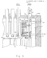
- Figure 5 shows a schematic plan view of the portion shown in Figure 3 and represents a plan view of a semiconductor device having the conventional LOC structure shown in Figure 1.
- Figure 5 highlights a problem with the conventional structure.
- 12 and 13 are inverters, 14 and 15 are nMOS transistors, 16 is a bonding pad, 17 is an external lead, and 18 is an external load.
- R1 through R3, L1, and C1 through C4 are respectively resistances, an inductance, and capacitances of the parasitic impedance to the signal path from the bonding pad 16 to the external lead 17.
- the external load 18 is exemplified by a model, comprising a capacitance CL, resistances R4 and R5 and current sources J1 and J2.
- R1 represents the resistance of the bonding wiring 9.
- C1 is equal to half the total capacitance of the wire bonding 9 plus the parasitic capacitance between the bonding pad 16 and the final stage (comprising a buffer including nMOS 14 and 15) of the output buffer 11.
- C2 is equal to half the capacitance of the wire bonding 9 and half the total capacitance of the inner lead 4.
- C3 is equal to half the total capacitance of the inner lead plus half the total capacitance of the external lead 17.
- C4 is half the total capacitance of the external lead 17.
- CL is the total capacitance of the external load 18.
- R2 is the resistance of the inner lead 4.
- R3 is the resistance of the external lead 5.
- L1 is the inductance of the line from an output buffer 11 of the final stage to the foremost end of external lead 17.
- Reference numeral 20 in Figure 3 represents a block obtained by dividing a memory cell array.
- the position of a bonding pad outputting a signal, and the length and area of an inner lead transmitting a signal, should be given more consideration in terms of the electrical characteristics than a bonding pad or an inner lead receiving a signal.
- an inner lead and a bonding pad transmitting a signal need to be configured to minimize the parasitic impedance components, i.e. R1, R2, R3, L1, and C1 through C4, shown in Figure 3 for the purpose of achieving high-speed access.
- a semiconductor device having the conventional LOC structure shown in Figure 1 such as the DRAM shown in Figure 3 treats an inner lead and a bonding pad transmitting a signal in the same way as it treats an inner lead and a bonding pad for solely receiving a signal, such that the bonding pad outputting a signal is arrayed in the direction of the longer side and near the middle of the element-formation surface 2 of the semiconductor chip 1 as shown in Figure 5.
- the tip 4BB of the inner lead 4B for outputting a signal is positioned on the top in the middle and in the direction of the longer side of the element-formation surface 2 of the semiconductor chip 1, as with the tip 4AA of the inner lead 4A for solely receiving a signal.
- a semiconductor device having the conventional LOC structure such as shown in Figure 1 has its signal paths 19 formed with kinked lines as shown in Figure 5, thereby preventing fast operation.
- 20 is a block split from a memory cell array
- 4A is an inner lead for solely receiving a signal
- 21A is a bonding pad for receiving a signal
- 21B is a bonding pad for transmitting a signal
- 4B is an inner lead for transmitting a signal.
- This invention aims at expending a data readout/write-in by providing a semiconductor device having a LOC structure with the least impedance parasitic to signal paths going to an external lead from a bonding pad for solely transmitting a signal or from a bonding pad for both transmitting and receiving a signal. Moreover it aims at further expediting high-speed readout with a shortened signal path.
- the feature of the present invention resides in a semiconductor device configured by attaching a semiconductor chip to a lead frame such that the tip of the inner lead of the lead frame is positioned on top of the element-formation surface of the semiconductor chip, and by resin-sealing a wire-bonding between the bonding pad of the semiconductor chip and the tip of the inner lead is performed.
- a bonding pad for solely receiving a signal is formed parallel to a perimeter on top in the middle of the element-formation surface.
- a bonding pad for solely transmitting a signal or for both receiving and transmitting a signal is formed near the periphery of the element-formation surface.
- An inner lead for solely receiving a signal has its tip positioned parallel to a perimeter on top in the middle of the element-formation surface in correspondence with the bonding pad for solely receiving a signal.
- An inner lead solely for transmitting a signal or for both receiving and transmitting a signal has its tip positioned on top of the periphery of the element-formation surface in correspondence with the bonding pad for solely transmitting a signal or for both receiving and transmitting a signal.
- FIG. 6 is a block diagram illustrating the underlying principles of this invention.
- 22 is a semiconductor chip
- 23 is an element-formation surface of the semiconductor chip 22
- 24 is a bonding pad for solely receiving a signal
- 25 is a bonding pad for solely transmitting a signal or for both receiving and transmitting a signal
- 26 is an inner lead for solely receiving a signal
- 27 is an inner lead for solely trnsmitting a signal or for both receiving and transmitting a signal
- 28 and 29 are bonding wires.
- the semiconductor device having the LOC structure pursuant to this invention is such that the bonding pad 24 for solely receiving a signal is formed near the middle along one side of the perimeter and the bonding pad 25 for solely transmitting a signal or for both receiving and transmitting a signal is formed near the periphery of the element-formation surface 23.
- the inner lead 26 for solely receiving a signal has its tip 26A positioned on top in the middle along one side of the perimeter of the element-formation surface 23, in correspondence with the bonding pad 24 for solely receiving a signal.
- the inner lead 27 for both receiving and transmitting a signal has its tip 27A positioned on top of the periphery of the element-formation surface 23, in correspondence with the bonding pad 25 solely for transmitting a signal or for both receiving and transmitting a signal.
- this invention makes a signal path shorter by short-cutting the turnaround part in a chip for a signal path compared with the conventional structure shown in Figure 5. Therefore, this invention further expedites readout.
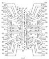
- Figure 7 shows a plan view showing a pertinent part of the first preferred embodiment.
- 32 is the main chip body
- 33 is the element-formation surface of the main chip body
- 34 through 41 are eight megabit [8M] blocks
- 42 through 77 are bonding pads
- 78 through 103 are inner leads.
- RAS ⁇ is a row address strobe signal
- CAS ⁇ is a column address strobe signal
- WE ⁇ is a write enable
- OE ⁇ is an output enable signal
- A0 through A11 are addresses
- DQ0 through DQ7 are data input/output terminals
- Vcc and Vss are power source voltages.
- bonding pads 42 through 77 bonding pads 43, 46, 51, 57, 62 and 69 are for a Vcc power source, and bonding pads 42, 48, 54, 59, 65 and 68 are for a Vss power source.
- bonding pads 44, 45, 47 and 49 are for receiving control signals ( WE ⁇ , CAS ⁇ , RAS ⁇ , and OE ⁇ ).
- bonding pads 50, 52, 53, 55, 56, 58, 60, 61, 63, 64, 66 and 67 are for receiving addresses (A0 to A12).
- bonding pads 70 through 77 are for both receiving and transmitting data (DQ0 to DQ7).
- inner lead 84 is for the Vcc power source
- inner lead 97 is for the Vss power source
- inner leads 78, 79, 102 and 103 are for receiving control signals ( WE ⁇ , RAS ⁇ , OE ⁇ and CAS ⁇ ).
- inner leads 81, 83, 85, 87, 89 through 92, 94, 96, 98 and 100 are for receiving addresses (A0 to A12), and inner leads 80, 82, 86, 88, 93, 95, 99 and 101 are for both receiving and transmitting data (DQ0 to DQ7).
- bonding pads 43, 46, 51, 57, 62 and 69 for the Vcc power source and bonding pads 42, 48, 54, 59, 65 and 68 for the Vss power source are formed in the direction of the longer side and in the middle of the element-formation surface 33.
- inner lead 84 for the Vcc power source and inner lead 97 for the Vss power source have their tips extended in the direction of the longer side and on top in the middle of the element-formation surface 33.
- the foremost ends of the inner leads 84 and 97 are provided opposite to each other with a predetermined interval.
- Bonding pads 44, 45, 47 and 49 for receiving control signals ( WE ⁇ , CAS ⁇ , RAS ⁇ and DE ⁇ ) and bonding pads 50, 52, 53, 55, 56, 58, 60, 61, 63, 64, 66 and 67 for receiving addresses are also formed in the direction of the longer side of the element-formation surface 33 and in the area under the area provided between the foremost end of the inner lead 84 and the foremost end of the inner lead 97 on top in the middle of the element-formation surface 33.
- inner leads 78, 79, 102 and 103 for receiving control signal and inner leads 81, 83, 85, 87, 89 through 92, 94, 96, 98 and 100 have their respective tips formed along the longitudinal direction on top of the center of the element-formation surface 33.
- inner leads 80, 82, 86, 88, 93, 95, 99, and 101 for both receiving and transmitting data have their respective tips formed on top of the periphery along the longitudinal direction of the element-formation surface 33.
- the circuitry formed along the longitudinal direction in the middle receives input signals, such as the row address strobe signal RAS ⁇ , the column address strobe signal CAS ⁇ , and addresses A0 through A11.
- the circuitry concentrates along the direction of the longer side and in the middle of the element-formation surface 33 and the power source has a low impedance due to the bus bar, the LOC structure is taken advantage of, and bonding pads provided in the middle of the element-formation surface 33 transmit access instruction signals to the eight megabit [8M] blocks 34 through 41.
- the access instruction signals are transmitted from the middle of the chip toward the chip periphery accompanied by a transmission delay of a word line, a transmission delay of a sense amplifier activation signal and a transmission delay of a column address, until they finally reach bonding pads 70 through 77 via output buffers near bonding pads 70 through 77 for both receiving and transmitting data signals and provided in the periphery of the element-formation surface 33. They are emitted to the outside via inner leads 80, 82, 86, 88, 93, 95 99 and 101 for both receiving and transmitting data signals.
- Bonding pads 70 through 77 for both receiving and transmitting data signals are formed on the periphery in the longitudinal direction. Also, because inner leads 80, 82, 86, 88, 93, 95, 99 and 101 have their respective tips formed on top of the periphery in the longitudinal direction of the element-formation surface 33 correspondingly, the overlaps between the element-formation surface 33 and inner leads 80, 82, 86, 88, 93, 95, 99 and 101 for both receiving and transmitting a data signal can be minimized.
- the shortening of the turnaround part for a signal path from an input signal to an output signal is effective in further expediting operations.
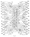
- Figure 8 shows a plan view showing a pertinent part of a second preferred embodiment.
- the second preferred embodiment aims at improving the impedance of the power source for an output buffer.
- bonding pads 104 and 105 for the Vcc power source are formed in a vicinity of eight megabit [8M] blocks 35 and 36 on the periphery of the element-formation surface 33, and that bonding pads 106 and 107 for the Vss power source are formed in a vicinity of eight megabit [8M] blocks 38 and 39 on the periphery of the element-formation surface 33.
- the second preferred embodiment configures everything else the same as the first preferred embodiment.
- bonding pads 104 and 105 for the Vcc power source are provided in a vicinity of eight megabit [8M] blocks 35 and 36 as well as in a central portion of the element-formation surface 33 and thus the impedance of the power source in an output buffer portion provided within blocks 35 and 36 can be more effectively decreased than in the first embodiment.
- the bonding pad for the Vss power source is provided in the vicinity of blocks 38 and 39 as well as in a central portion of the element-formation surface 33, and the impedance of the power source in the output buffer portion provided within blocks 38 and 39 can be more effectively decreased than in the first preferred embodiment. Therefore, the data signals DQ1, DQ2, DQ6 and DQ7 can be read/written with a speed higher than in the first embodiment.
- Figure 9 shows a plan view showing a pertinent part of a third preferred embodiment.
- the third embodiment aims at further improving the impedance of the power source of an output buffer beyond the second embodiment.
- bonding pads 108 through 112 for the Vcc power source are formed near eight megabit [8M] blocks 34, 37, 38, 40 and 41 (shown in Figures 7 and 8 but not shown in Figure 9) on the periphery of the element-formation surface 33, that bonding pads 113 through 117 for the Vss power source are formed near eight megabit [8M] blocks 34, 36, 37, 38 and 41 (shown in Figures 7 and 8 but not shown in Figure 9) on the periphery of the element-formation surface 33, and that bonding pad 104 for the Vcc power source and bonding pad 106 for the Vss power source are not formed.
- the third preferred embodiment configures everything else the same as the second preferred embodiment.
- the bonding pads for the Vcc power source are further provided in the vicinity of blocks 34, 37, 38, 40 and 41 and the bonding pads for the Vss power source are provided in the vicinity of the blocks 34, 37, 38, 40 and 41 and thus the impedance of the power source in the output buffer portion of blocks 34, 37, 38, 40 and 41 can be decreased more effectively than in the second embodiment. Therefore, a read/write for the data signal DQ0, DQ3, DQ4, DQ5 and DQ7 can be performed with a higher speed than in the second embodiment.
- Figure 10 shows a plan view showing a pertinent part of a fourth preferred embodiment.
- the fourth embodiment is such that bonding pads 43 and 69 for the Vcc power source, bonding pads 42 and 68 for the Vss power source, bonding pads 44, 45, 47 and 49 for receiving control signals, and bonding pads 50, 52, 53, 55, 56, 58, 60, 61, 63, 64, 66 and 67 are formed in the width direction, namely, in the direction of the shorter side near the center of the element-formation surface 33, and that bonding pads 70 through 77 for both receiving and transmitting data signals are formed on the short sides of the perimeter of the element-formation surface 33.
- inner lead 84 for the Vcc power source has its tip extended, namely, across the width on top near the center of the element-formation surface 33.
- Inner leads 78, 79, 102 and 103 for receiving control signals WE ⁇ , RAS ⁇ , DE ⁇ and CAS ⁇ , and inner leads for 81, 83, 85, 87, 89 through 92, 94, 96, 98 and 100 for receiving address signals A0 through A11 have their tips positioned along the short side on top near the center of the element-formation surface 33.
- Inner leads 80, 82, 86, 88, 93, 95, 99 and 101 for both receiving and transmitting data signals DQ0 through DQ7 have their tips positioned along the short sides of the perimeter on top of the element-formation surface 33.
- the fourth embodiment can achieve advantages similar to the third embodiment.
- this invention enables the overlap between an element-formation surface and an inner lead for solely transmitting a signal or for both receiving and transmitting a signal, it is effective in reducing the parasitic impedance to signal paths going to an external lead from a bonding pad, and expediting a read/write operation. Moreover shortening the turnaround part of the signal path further expedites a read/write.
Landscapes
- Engineering & Computer Science (AREA)
- Computer Hardware Design (AREA)
- Microelectronics & Electronic Packaging (AREA)
- Power Engineering (AREA)
- Physics & Mathematics (AREA)
- Condensed Matter Physics & Semiconductors (AREA)
- General Physics & Mathematics (AREA)
- Semiconductor Integrated Circuits (AREA)
- Dram (AREA)
- Lead Frames For Integrated Circuits (AREA)
- Design And Manufacture Of Integrated Circuits (AREA)
Abstract
Description
- This invention pertains to a semiconductor device having a so-called LOC (Lead on Chip) structure.
- The LOC structure is configured by connecting to an upper surface of a semiconductor chip, an inner lead of a lead frame using a bonding agent, i.e. by attaching the semiconductor chip and the lead frame, such that the tip of the inner lead of the lead frame is positioned on top of the element-formation surface of the semiconductor chip. The bonding pad of the semiconductor chip and the tip of the inner lead are wire-bonded and resin-sealed.
- Adopting the LOC structure gives increased electrical advantages and enables a chip with a large size to be installed in a small relatively package.
- Regarding the electrical advantages, it becomes possible to perform wire bonding of the inner lead (for example, a bus-bar-lead) to be used as an electric power line or a ground line separately from the inner lead to be used for each circuit block such as a sense amplifier and
input section 3. The result is as follows. - 1. The AL (Aluminum) wiring in a chip can be shortened and speeded up.
- 2. The layout design of each circuit block in a chip is facilitated, and thus a semiconductor device structure with an increased number of bits can be easily developed.
- 3. Since the bus-bar-lead is used for wiring, the resistance of the AL wiring can be decreased thereby enabling a semiconductor device suitable for high-speed operation to be provided.
- 4. Since the number of bonding wires can be freely selected, it becomes possible to decrease the noise caused during operation of the sense amplifier for reading out data.
- The LOC structure is also advantageous in that it can be inserted in a package with a predetermined size. Namely, the conventional package structure requires a large space for the wiring leads around a semiconductor chip but in contrast, the LOC structure can increase the ratio of the area of the chip to that of the package.
- Figure 1 is a slant view of a semiconductor device having a conventional LOC structure.
- Figure 2 shows an A-A cutaway of the semiconductor device having the conventional LOC structure shown in Figure 1.
- In Figures 1 and 2, 1 is a semiconductor chip (an LSI chip), 2 is an element-formation surface for the
semiconductor chip lead frame lead frame semiconductor chip 1 to thelead frame 3. - Also, 7 is the bus bar around the inner leads for a Vcc power source, 8 is the bus bar around the inner leads for a Vss power source, 9 is a bonding wire comprised of an Au wire, and 10 is a molding resin.
- Such LOC structured semiconductor devices have been developed mainly as a technique for packaging DRAMs (Dynamic Random Access Memory) with capacities between four megabits [4M] and sixteen megabits [16M] for example, at the present and SRAMs (Static Random Access Memory) of four megabits [ 4M ], for example, at the present. It removes from the conventional lead frame a part called a die-pad for loading a semiconductor chip and has an inner lead extended on to the element-formation surface of the semiconductor chip.
- Also, the semiconductor device shown in Figure 1 has the
bus bars - Figure 3 shows a portion of a DRAM with a conventional LOC structure. Figure 4 shows an equivalent circuit for the portion shown in Figure 3 and represents a circuit diagram for an output stage of the semiconductor device having the conventional LOC structure shown in Figure 1. Figure 4 highlights the problems with the conventional structure. Figure 5 shows a schematic plan view of the portion shown in Figure 3 and represents a plan view of a semiconductor device having the conventional LOC structure shown in Figure 1. Figure 5 highlights a problem with the conventional structure.
- With the recent trend of increasing the number of bits in a DRAM,
multiple output buffers 11 loaded on a semiconductor chip has increased from eight [8], to sixteen [16], to thirty-two [32], ..... - In Figure 4, 12 and 13 are inverters, 14 and 15 are nMOS transistors, 16 is a bonding pad, 17 is an external lead, and 18 is an external load. R1 through R3, L1, and C1 through C4 are respectively resistances, an inductance, and capacitances of the parasitic impedance to the signal path from the
bonding pad 16 to theexternal lead 17. Theexternal load 18 is exemplified by a model, comprising a capacitance CL, resistances R4 and R5 and current sources J1 and J2. - As shown in Figure 3, R1 represents the resistance of the
bonding wiring 9. C1 is equal to half the total capacitance of the wire bonding 9 plus the parasitic capacitance between thebonding pad 16 and the final stage (comprising abuffer including nMOS 14 and 15) of theoutput buffer 11. C2 is equal to half the capacitance of the wire bonding 9 and half the total capacitance of theinner lead 4. C3 is equal to half the total capacitance of the inner lead plus half the total capacitance of theexternal lead 17. C4 is half the total capacitance of theexternal lead 17. CL is the total capacitance of theexternal load 18. R2 is the resistance of theinner lead 4. R3 is the resistance of theexternal lead 5. L1 is the inductance of the line from anoutput buffer 11 of the final stage to the foremost end ofexternal lead 17.Reference numeral 20 in Figure 3 represents a block obtained by dividing a memory cell array. - Since noise generated when the multiple (eight [8], sixteen [16], thirty-two [32], ....)
output buffers 11 simultaneously switch, cannot be borne by the power source line alone, an effective countermeasure for the noise has been sought. - The position of a bonding pad outputting a signal, and the length and area of an inner lead transmitting a signal, should be given more consideration in terms of the electrical characteristics than a bonding pad or an inner lead receiving a signal.
- That is, it should be kept in mind that an inner lead and a bonding pad transmitting a signal need to be configured to minimize the parasitic impedance components, i.e. R1, R2, R3, L1, and C1 through C4, shown in Figure 3 for the purpose of achieving high-speed access.
- However, a semiconductor device having the conventional LOC structure shown in Figure 1 such as the DRAM shown in Figure 3 treats an inner lead and a bonding pad transmitting a signal in the same way as it treats an inner lead and a bonding pad for solely receiving a signal, such that the bonding pad outputting a signal is arrayed in the direction of the longer side and near the middle of the element-
formation surface 2 of thesemiconductor chip 1 as shown in Figure 5. Moreover the tip 4BB of the inner lead 4B for outputting a signal is positioned on the top in the middle and in the direction of the longer side of the element-formation surface 2 of thesemiconductor chip 1, as with the tip 4AA of theinner lead 4A for solely receiving a signal. - Accordingly, the values of parasitic impedance components, i.e. R1, R2, R3, L1, and C1 through C4, become large, thereby causing the problem of delaying signal transmission and inhibiting expeditious readout.
- Also, a semiconductor device having the conventional LOC structure such as shown in Figure 1 has its
signal paths 19 formed with kinked lines as shown in Figure 5, thereby preventing fast operation. In Figure 5, 20 is a block split from a memory cell array, 4A is an inner lead for solely receiving a signal, 21A is a bonding pad for receiving a signal, 21B is a bonding pad for transmitting a signal, and 4B is an inner lead for transmitting a signal. - This invention aims at expending a data readout/write-in by providing a semiconductor device having a LOC structure with the least impedance parasitic to signal paths going to an external lead from a bonding pad for solely transmitting a signal or from a bonding pad for both transmitting and receiving a signal. Moreover it aims at further expediting high-speed readout with a shortened signal path.
- The feature of the present invention resides in a semiconductor device configured by attaching a semiconductor chip to a lead frame such that the tip of the inner lead of the lead frame is positioned on top of the element-formation surface of the semiconductor chip, and by resin-sealing a wire-bonding between the bonding pad of the semiconductor chip and the tip of the inner lead is performed. A bonding pad for solely receiving a signal is formed parallel to a perimeter on top in the middle of the element-formation surface. A bonding pad for solely transmitting a signal or for both receiving and transmitting a signal is formed near the periphery of the element-formation surface. An inner lead for solely receiving a signal has its tip positioned parallel to a perimeter on top in the middle of the element-formation surface in correspondence with the bonding pad for solely receiving a signal. An inner lead solely for transmitting a signal or for both receiving and transmitting a signal has its tip positioned on top of the periphery of the element-formation surface in correspondence with the bonding pad for solely transmitting a signal or for both receiving and transmitting a signal.
- One skilled in the art can easily understand additional features and objects of this invention from the description of the preferred embodiments and some of the attached drawings. In the drawings:
- Figure 1 is a slant view of an entire configuration of a semiconductor device having the conventional LOC structure;
- Figure 2 shows an A-A cutaway of the semiconductor device having the conventional LOC structure shown in Figure 1;
- Figure 3 shows a plan view of a DRAM with the conventional LOC structure;
- Figure 4 is a circuit diagram for the semiconductor device having the conventional LOC structure shown in Figure 3. It highlights the problems of the conventional structure;
- Figure 5 shows a plan view of the semiconductor device having the conventional LOC structure shown in Figure 1 and highlights its problems;
- Figure 6 is a block diagram illustrating the underlying principles of this invention;
- Figure 7 shows a plan view showing a pertinent part of a first preferred embodiment;
- Figure 8 shows a plan view showing a pertinent part of a second preferred embodiment;
- Figure 9 shows a plan view showing a pertinent part of a third preferred embodiment; and
- Figure 10 shows a plan view showing a pertinent part of a fourth preferred embodiment.
- Before going into the details of an explanation of some preferred embodiments, the underlying principles of this invention are explained below.
- Figure 6 is a block diagram illustrating the underlying principles of this invention.
- In Figure 6, 22 is a semiconductor chip, 23 is an element-formation surface of the
semiconductor chip - The semiconductor device having the LOC structure pursuant to this invention is such that the
bonding pad 24 for solely receiving a signal is formed near the middle along one side of the perimeter and thebonding pad 25 for solely transmitting a signal or for both receiving and transmitting a signal is formed near the periphery of the element-formation surface 23. - Therefore, the
inner lead 26 for solely receiving a signal has itstip 26A positioned on top in the middle along one side of the perimeter of the element-formation surface 23, in correspondence with thebonding pad 24 for solely receiving a signal. Theinner lead 27 for both receiving and transmitting a signal has itstip 27A positioned on top of the periphery of the element-formation surface 23, in correspondence with thebonding pad 25 solely for transmitting a signal or for both receiving and transmitting a signal. - As shown in Figure 5, this invention makes a signal path shorter by short-cutting the turnaround part in a chip for a signal path compared with the conventional structure shown in Figure 5. Therefore, this invention further expedites readout.
- Explained below with reference to Figures 7 through 10, are the first through the fourth preferred embodiments of this invention, each illustrating a sixty-four megabit (64M) DRAM to which this invention is applied.
- Figure 7 shows a plan view showing a pertinent part of the first preferred embodiment.
- In Figure 7, 32 is the main chip body, 33 is the element-formation surface of the
main chip body - Also,


- Of the
bonding pads 42 through 77,bonding pads bonding pads - Also,
bonding pads 


bonding pads bonding pads 70 through 77 are for both receiving and transmitting data (DQ0 to DQ7). - Of the inner leads 78 through 103,
inner lead 84 is for the Vcc power source,inner lead 97 is for the Vss power source, inner leads 78, 79, 102 and 103 are for receiving control signals (


- Also, inner leads 81, 83, 85, 87, 89 through 92, 94, 96, 98 and 100 are for receiving addresses (A0 to A12), and inner leads 80, 82, 86, 88, 93, 95, 99 and 101 are for both receiving and transmitting data (DQ0 to DQ7).
- That is, as is evident from Figure 6,
bonding pads bonding pads formation surface 33. - Consequently,
inner lead 84 for the Vcc power source andinner lead 97 for the Vss power source have their tips extended in the direction of the longer side and on top in the middle of the element-formation surface 33. The foremost ends of the inner leads 84 and 97 are provided opposite to each other with a predetermined interval. -
Bonding pads 


bonding pads formation surface 33 and in the area under the area provided between the foremost end of theinner lead 84 and the foremost end of theinner lead 97 on top in the middle of the element-formation surface 33. - Hence, in correspondence with those bonding pads, inner leads 78, 79, 102 and 103 for receiving control signal and
inner leads formation surface 33. - As well, in correspondence with the positions at which
bonding pads 70 through 77 are formed, inner leads 80, 82, 86, 88, 93, 95, 99, and 101 for both receiving and transmitting data (DQ0 through DQ7) have their respective tips formed on top of the periphery along the longitudinal direction of the element-formation surface 33. - Thus, in the first embodiment, the circuitry formed along the longitudinal direction in the middle receives input signals, such as the row address strobe signal


- Because the circuitry concentrates along the direction of the longer side and in the middle of the element-
formation surface 33 and the power source has a low impedance due to the bus bar, the LOC structure is taken advantage of, and bonding pads provided in the middle of the element-formation surface 33 transmit access instruction signals to the eight megabit [8M] blocks 34 through 41. - The access instruction signals are transmitted from the middle of the chip toward the chip periphery accompanied by a transmission delay of a word line, a transmission delay of a sense amplifier activation signal and a transmission delay of a column address, until they finally reach
bonding pads 70 through 77 via output buffers nearbonding pads 70 through 77 for both receiving and transmitting data signals and provided in the periphery of the element-formation surface 33. They are emitted to the outside via inner leads 80, 82, 86, 88, 93, 95 99 and 101 for both receiving and transmitting data signals. -
Bonding pads 70 through 77 for both receiving and transmitting data signals are formed on the periphery in the longitudinal direction. Also, because inner leads 80, 82, 86, 88, 93, 95, 99 and 101 have their respective tips formed on top of the periphery in the longitudinal direction of the element-formation surface 33 correspondingly, the overlaps between the element-formation surface 33 and inner leads 80, 82, 86, 88, 93, 95, 99 and 101 for both receiving and transmitting a data signal can be minimized. - As a result, the impedances parasitic to the signal paths going to external leads from
bonding pads 70 through 77 for both receiving and transmitting data signals are minimized, thereby expediting readout. - Also, the shortening of the turnaround part for a signal path from an input signal to an output signal is effective in further expediting operations.
- Figure 8 shows a plan view showing a pertinent part of a second preferred embodiment.
- The second preferred embodiment aims at improving the impedance of the power source for an output buffer. What make the second preferred embodiment distinct from the first preferred embodiment are that bonding
pads formation surface 33, and thatbonding pads formation surface 33. The second preferred embodiment configures everything else the same as the first preferred embodiment. - Namely, in the second preferred embodiment,
bonding pads formation surface 33 and thus the impedance of the power source in an output buffer portion provided withinblocks blocks formation surface 33, and the impedance of the power source in the output buffer portion provided withinblocks - Figure 9 shows a plan view showing a pertinent part of a third preferred embodiment.
- The third embodiment aims at further improving the impedance of the power source of an output buffer beyond the second embodiment. What make the third preferred embodiment distinct from the second preferred embodiment are that bonding
pads 108 through 112 for the Vcc power source are formed near eight megabit [8M] blocks 34, 37, 38, 40 and 41 (shown in Figures 7 and 8 but not shown in Figure 9) on the periphery of the element-formation surface 33, thatbonding pads 113 through 117 for the Vss power source are formed near eight megabit [8M] blocks 34, 36, 37, 38 and 41 (shown in Figures 7 and 8 but not shown in Figure 9) on the periphery of the element-formation surface 33, and thatbonding pad 104 for the Vcc power source andbonding pad 106 for the Vss power source are not formed. The third preferred embodiment configures everything else the same as the second preferred embodiment. - In the third embodiment, the bonding pads for the Vcc power source are further provided in the vicinity of
blocks blocks blocks - Figure 10 shows a plan view showing a pertinent part of a fourth preferred embodiment.
- The fourth embodiment is such that
bonding pads bonding pads bonding pads bonding pads formation surface 33, and thatbonding pads 70 through 77 for both receiving and transmitting data signals are formed on the short sides of the perimeter of the element-formation surface 33. - Correspondingly,
inner lead 84 for the Vcc power source has its tip extended, namely, across the width on top near the center of the element-formation surface 33. - Inner leads 78, 79, 102 and 103 for receiving control signals


formation surface 33. - Inner leads 80, 82, 86, 88, 93, 95, 99 and 101 for both receiving and transmitting data signals DQ0 through DQ7 have their tips positioned along the short sides of the perimeter on top of the element-
formation surface 33. Thus, the fourth embodiment can achieve advantages similar to the third embodiment. - As described above, since this invention enables the overlap between an element-formation surface and an inner lead for solely transmitting a signal or for both receiving and transmitting a signal, it is effective in reducing the parasitic impedance to signal paths going to an external lead from a bonding pad, and expediting a read/write operation. Moreover shortening the turnaround part of the signal path further expedites a read/write.
Claims (8)
- A semiconductor device configured by attaching a semiconductor chip to a lead frame such that the tip of an inner lead of said lead frame is positioned on top of an element-formation surface of a semiconductor chip (22), and by resin-sealing a wire-bonding between a bonding pad of said semiconductor chip and said tip of said inner lead, comprising:
a bonding pad (24) solely for receiving a signal and which is formed parallel to a perimeter on top in the middle of the said element-formation surface;
a bonding pad (25) solely for transmitting a signal or both for receiving and transmitting a signal and which is formed around the periphery of the said element-formation surface;
an inner lead (26) solely for receiving a signal and which has its tip positioned parallel to the perimeter on top in the middle of the said element-formation surface in correspondence with the said bonding pad solely for receiving a signal;
an inner lead (27) solely for transmitting a signal or both for receiving and transmitting a signal and which has its tip positioned on top of the periphery of the said element-formation surface in correspondence with the said bonding pad solely for transmitting a signal or both for receiving and transmitting a signal. - The semiconductor device according to Claim 1 wherein:
the bonding pad solely for receiving a signal is provided parallel to the longer side and in the middle of the element-formation surface. - The semiconductor device according to Claim 1 wherein:
the bonding pad solely for receiving a signal is provided in a direction of the shorter side and in the middle of the element-formation surface. - The semiconductor device according to Claim 1 wherein:
the bonding pad solely for receiving signal formed in the center of the element-formation surface includes a bonding pad for inputting power. - The semiconductor device according to Claim 1, wherein:
the bonding pads for supplying power to output buffers for output signals are formed near the periphery of the said element-formation surface, in correspondence with at least some of said output buffers; and
inner leads for the source are formed corresponding to the said bonding pads thus formed. - The semiconductor device according to Claim 5 wherein:
the bonding pad solely for receiving a signal is provided in a direction of a longer side in the middle of the element-formation surface. - The semiconductor device according to Claim 2 wherein:
the bonding pad solely for receiving the signal is provided in a direction of a shorter side in the middle of the said element-formation surface. - The semiconductor device according to Claim 2 wherein:
the bonding pad solely for receiving a signal formed in the middle of said element-formation surface includes a bonding pad for inputting power.
Applications Claiming Priority (2)
| Application Number | Priority Date | Filing Date | Title |
|---|---|---|---|
| JP3241045A JP2932785B2 (en) | 1991-09-20 | 1991-09-20 | Semiconductor device |
| JP241045/91 | 1991-09-20 |
Publications (2)
| Publication Number | Publication Date |
|---|---|
| EP0533589A1 true EP0533589A1 (en) | 1993-03-24 |
| EP0533589B1 EP0533589B1 (en) | 1998-08-26 |
Family
ID=17068492
Family Applications (1)
| Application Number | Title | Priority Date | Filing Date |
|---|---|---|---|
| EP92402587A Expired - Lifetime EP0533589B1 (en) | 1991-09-20 | 1992-09-21 | A semiconductor device |
Country Status (5)
| Country | Link |
|---|---|
| US (1) | US5648680A (en) |
| EP (1) | EP0533589B1 (en) |
| JP (1) | JP2932785B2 (en) |
| KR (1) | KR960003767B1 (en) |
| DE (1) | DE69226742T2 (en) |
Cited By (6)
| Publication number | Priority date | Publication date | Assignee | Title |
|---|---|---|---|---|
| EP0576021A1 (en) * | 1992-06-24 | 1993-12-29 | Kabushiki Kaisha Toshiba | Lead on chip structure for semiconductor device |
| GB2278956B (en) * | 1993-06-09 | 1997-10-08 | At & T Corp | Integrated circuit with multiple relative offset bond pad array |
| GB2312988A (en) * | 1996-05-10 | 1997-11-12 | Memory Corp Plc | Connecting a semiconductor die to a carrier |
| GB2320616A (en) * | 1996-12-18 | 1998-06-24 | Hyundai Electronics Ind | Semiconductor chip package |
| EP0962976A2 (en) * | 1998-06-03 | 1999-12-08 | Hewlett-Packard Company | Intergrated circuit having unique lead configuration |
| US6781220B2 (en) | 2001-05-30 | 2004-08-24 | Infineon Technologies Ag | Printed circuit board for semiconductor memory device |
Families Citing this family (8)
| Publication number | Priority date | Publication date | Assignee | Title |
|---|---|---|---|---|
| US5384487A (en) * | 1993-05-05 | 1995-01-24 | Lsi Logic Corporation | Off-axis power branches for interior bond pad arrangements |
| KR0179924B1 (en) * | 1996-06-14 | 1999-03-20 | 문정환 | Bottom lead semiconductor package |
| JP3036498B2 (en) * | 1997-12-08 | 2000-04-24 | 日本電気株式会社 | Semiconductor package |
| US6268643B1 (en) | 1997-12-22 | 2001-07-31 | Texas Instruments Incorporated | Lead frame device for delivering electrical power to a semiconductor die |
| TW530525B (en) * | 2001-07-27 | 2003-05-01 | Via Tech Inc | Method of disposing buffer and its chip |
| US7489026B2 (en) * | 2006-10-31 | 2009-02-10 | Freescale Semiconductor, Inc. | Methods and apparatus for a Quad Flat No-Lead (QFN) package |
| US11631623B2 (en) * | 2018-09-06 | 2023-04-18 | Mitsubishi Electric Corporation | Power semiconductor device and method of manufacturing the same, and power conversion device |
| JPWO2020059751A1 (en) | 2018-09-19 | 2021-08-30 | ローム株式会社 | Semiconductor device |
Citations (4)
| Publication number | Priority date | Publication date | Assignee | Title |
|---|---|---|---|---|
| EP0198194A1 (en) * | 1985-04-18 | 1986-10-22 | International Business Machines Corporation | Packaged semiconductor chip |
| EP0204177A1 (en) * | 1985-05-31 | 1986-12-10 | Siemens Aktiengesellschaft | Connection arrangement for semiconductor integrated circuits |
| EP0295459A2 (en) * | 1987-06-15 | 1988-12-21 | International Business Machines Corporation | Electronic assembly and method of making it |
| US4951122A (en) * | 1987-05-27 | 1990-08-21 | Hitachi, Ltd. | Resin-encapsulated semiconductor device |
Family Cites Families (2)
| Publication number | Priority date | Publication date | Assignee | Title |
|---|---|---|---|---|
| KR0158868B1 (en) * | 1988-09-20 | 1998-12-01 | 미다 가쓰시게 | Semiconductor device |
| US5151559A (en) * | 1991-05-02 | 1992-09-29 | International Business Machines Corporation | Planarized thin film surface covered wire bonded semiconductor package |
-
1991
- 1991-09-20 JP JP3241045A patent/JP2932785B2/en not_active Expired - Fee Related
-
1992
- 1992-09-21 DE DE69226742T patent/DE69226742T2/en not_active Expired - Fee Related
- 1992-09-21 EP EP92402587A patent/EP0533589B1/en not_active Expired - Lifetime
- 1992-09-21 KR KR1019920017207A patent/KR960003767B1/en not_active IP Right Cessation
-
1995
- 1995-09-29 US US08/536,674 patent/US5648680A/en not_active Expired - Fee Related
Patent Citations (4)
| Publication number | Priority date | Publication date | Assignee | Title |
|---|---|---|---|---|
| EP0198194A1 (en) * | 1985-04-18 | 1986-10-22 | International Business Machines Corporation | Packaged semiconductor chip |
| EP0204177A1 (en) * | 1985-05-31 | 1986-12-10 | Siemens Aktiengesellschaft | Connection arrangement for semiconductor integrated circuits |
| US4951122A (en) * | 1987-05-27 | 1990-08-21 | Hitachi, Ltd. | Resin-encapsulated semiconductor device |
| EP0295459A2 (en) * | 1987-06-15 | 1988-12-21 | International Business Machines Corporation | Electronic assembly and method of making it |
Cited By (9)
| Publication number | Priority date | Publication date | Assignee | Title |
|---|---|---|---|---|
| EP0576021A1 (en) * | 1992-06-24 | 1993-12-29 | Kabushiki Kaisha Toshiba | Lead on chip structure for semiconductor device |
| US5391918A (en) * | 1992-06-24 | 1995-02-21 | Kabushiki Kaisha Toshiba | Semiconductor device |
| GB2278956B (en) * | 1993-06-09 | 1997-10-08 | At & T Corp | Integrated circuit with multiple relative offset bond pad array |
| GB2312988A (en) * | 1996-05-10 | 1997-11-12 | Memory Corp Plc | Connecting a semiconductor die to a carrier |
| GB2320616A (en) * | 1996-12-18 | 1998-06-24 | Hyundai Electronics Ind | Semiconductor chip package |
| GB2320616B (en) * | 1996-12-18 | 2002-01-16 | Hyundai Electronics Ind | An improved chip-size package semiconductor |
| EP0962976A2 (en) * | 1998-06-03 | 1999-12-08 | Hewlett-Packard Company | Intergrated circuit having unique lead configuration |
| EP0962976A3 (en) * | 1998-06-03 | 2000-05-10 | Hewlett-Packard Company | Intergrated circuit having unique lead configuration |
| US6781220B2 (en) | 2001-05-30 | 2004-08-24 | Infineon Technologies Ag | Printed circuit board for semiconductor memory device |
Also Published As
| Publication number | Publication date |
|---|---|
| KR960003767B1 (en) | 1996-03-22 |
| DE69226742D1 (en) | 1998-10-01 |
| US5648680A (en) | 1997-07-15 |
| DE69226742T2 (en) | 1999-01-14 |
| EP0533589B1 (en) | 1998-08-26 |
| JP2932785B2 (en) | 1999-08-09 |
| JPH0582703A (en) | 1993-04-02 |
| KR930006889A (en) | 1993-04-22 |
Similar Documents
| Publication | Publication Date | Title |
|---|---|---|
| US6625050B2 (en) | Semiconductor memory device adaptable to various types of packages | |
| US5357478A (en) | Semiconductor integrated circuit device including a plurality of cell array blocks | |
| US6593646B2 (en) | Dual die memory | |
| EP0533589B1 (en) | A semiconductor device | |
| US6353549B1 (en) | Architecture and package orientation for high speed memory devices | |
| JP3137749B2 (en) | Semiconductor integrated circuit device | |
| US7227251B2 (en) | Semiconductor device and a memory system including a plurality of IC chips in a common package | |
| US5587607A (en) | Semiconductor integrated circuit device having improvement arrangement of pads | |
| US5789808A (en) | Semiconductor device structured to be less susceptible to power supply noise | |
| US5900021A (en) | Pad input select circuit for use with bond options | |
| US20030089926A1 (en) | Semiconductor device | |
| KR100224770B1 (en) | Lead on chip type lead frame and semiconductor package using it | |
| US5998869A (en) | High storage capacity, wide data input/output channel, static random access memory device | |
| KR100481184B1 (en) | Semiconductor memory integrated circuit | |
| JP2985479B2 (en) | Semiconductor memory and semiconductor memory module | |
| JP3911365B2 (en) | Semiconductor memory device | |
| KR100306967B1 (en) | Arrangement of data input/output circuits for use in a semiconductor memory integrated circuit device | |
| KR0175022B1 (en) | Data input / output mode converter of semiconductor memory device | |
| KR100192588B1 (en) | Semiconductor memory device having partial chip | |
| KR19980034266A (en) | Bank separation method of semiconductor memory device and device therefor | |
| JPH0358544B2 (en) | ||
| JPH04284636A (en) | Semiconductor device |
Legal Events
| Date | Code | Title | Description |
|---|---|---|---|
| PUAI | Public reference made under article 153(3) epc to a published international application that has entered the european phase |
Free format text: ORIGINAL CODE: 0009012 |
|
| AK | Designated contracting states |
Kind code of ref document: A1 Designated state(s): DE FR GB IT |
|
| 17P | Request for examination filed |
Effective date: 19930903 |
|
| 17Q | First examination report despatched |
Effective date: 19950403 |
|
| GRAG | Despatch of communication of intention to grant |
Free format text: ORIGINAL CODE: EPIDOS AGRA |
|
| GRAG | Despatch of communication of intention to grant |
Free format text: ORIGINAL CODE: EPIDOS AGRA |
|
| GRAH | Despatch of communication of intention to grant a patent |
Free format text: ORIGINAL CODE: EPIDOS IGRA |
|
| GRAH | Despatch of communication of intention to grant a patent |
Free format text: ORIGINAL CODE: EPIDOS IGRA |
|
| GRAA | (expected) grant |
Free format text: ORIGINAL CODE: 0009210 |
|
| AK | Designated contracting states |
Kind code of ref document: B1 Designated state(s): DE FR GB IT |
|
| REF | Corresponds to: |
Ref document number: 69226742 Country of ref document: DE Date of ref document: 19981001 |
|
| ET | Fr: translation filed | ||
| PLBE | No opposition filed within time limit |
Free format text: ORIGINAL CODE: 0009261 |
|
| STAA | Information on the status of an ep patent application or granted ep patent |
Free format text: STATUS: NO OPPOSITION FILED WITHIN TIME LIMIT |
|
| 26N | No opposition filed | ||
| REG | Reference to a national code |
Ref country code: GB Ref legal event code: IF02 |
|
| PGFP | Annual fee paid to national office [announced via postgrant information from national office to epo] |
Ref country code: DE Payment date: 20070913 Year of fee payment: 16 |
|
| PGFP | Annual fee paid to national office [announced via postgrant information from national office to epo] |
Ref country code: GB Payment date: 20070919 Year of fee payment: 16 |
|
| PGFP | Annual fee paid to national office [announced via postgrant information from national office to epo] |
Ref country code: IT Payment date: 20070926 Year of fee payment: 16 |
|
| PGFP | Annual fee paid to national office [announced via postgrant information from national office to epo] |
Ref country code: FR Payment date: 20070914 Year of fee payment: 16 |
|
| GBPC | Gb: european patent ceased through non-payment of renewal fee |
Effective date: 20080921 |
|
| REG | Reference to a national code |
Ref country code: FR Ref legal event code: ST Effective date: 20090529 |
|
| PG25 | Lapsed in a contracting state [announced via postgrant information from national office to epo] |
Ref country code: IT Free format text: LAPSE BECAUSE OF NON-PAYMENT OF DUE FEES Effective date: 20080921 Ref country code: DE Free format text: LAPSE BECAUSE OF NON-PAYMENT OF DUE FEES Effective date: 20090401 |
|
| PG25 | Lapsed in a contracting state [announced via postgrant information from national office to epo] |
Ref country code: FR Free format text: LAPSE BECAUSE OF NON-PAYMENT OF DUE FEES Effective date: 20080930 |
|
| PG25 | Lapsed in a contracting state [announced via postgrant information from national office to epo] |
Ref country code: GB Free format text: LAPSE BECAUSE OF NON-PAYMENT OF DUE FEES Effective date: 20080921 |