EP0525617B1 - Liquid-phase growth process of compound semiconductor - Google Patents
Liquid-phase growth process of compound semiconductor Download PDFInfo
- Publication number
- EP0525617B1 EP0525617B1 EP92112538A EP92112538A EP0525617B1 EP 0525617 B1 EP0525617 B1 EP 0525617B1 EP 92112538 A EP92112538 A EP 92112538A EP 92112538 A EP92112538 A EP 92112538A EP 0525617 B1 EP0525617 B1 EP 0525617B1
- Authority
- EP
- European Patent Office
- Prior art keywords
- phase growth
- liquid
- surface defect
- hydrogen
- hole
- Prior art date
- Legal status (The legal status is an assumption and is not a legal conclusion. Google has not performed a legal analysis and makes no representation as to the accuracy of the status listed.)
- Expired - Lifetime
Links
- 239000007791 liquid phase Substances 0.000 title claims description 30
- 238000000034 method Methods 0.000 title claims description 25
- 239000004065 semiconductor Substances 0.000 title claims description 7
- 150000001875 compounds Chemical class 0.000 title claims description 6
- UFHFLCQGNIYNRP-UHFFFAOYSA-N Hydrogen Chemical compound [H][H] UFHFLCQGNIYNRP-UHFFFAOYSA-N 0.000 claims description 23
- 239000000758 substrate Substances 0.000 claims description 17
- XKRFYHLGVUSROY-UHFFFAOYSA-N Argon Chemical compound [Ar] XKRFYHLGVUSROY-UHFFFAOYSA-N 0.000 claims description 16
- 239000001257 hydrogen Substances 0.000 claims description 16
- 229910052739 hydrogen Inorganic materials 0.000 claims description 16
- 239000007789 gas Substances 0.000 claims description 13
- 239000000203 mixture Substances 0.000 claims description 12
- 229910052786 argon Inorganic materials 0.000 claims description 8
- 239000013078 crystal Substances 0.000 claims description 7
- 239000011261 inert gas Substances 0.000 claims description 6
- 230000007547 defect Effects 0.000 description 34
- 238000002844 melting Methods 0.000 description 6
- 230000008018 melting Effects 0.000 description 6
- 239000000155 melt Substances 0.000 description 5
- 238000011179 visual inspection Methods 0.000 description 5
- 230000000052 comparative effect Effects 0.000 description 4
- 238000004519 manufacturing process Methods 0.000 description 4
- 230000000694 effects Effects 0.000 description 3
- 238000011109 contamination Methods 0.000 description 2
- 238000007598 dipping method Methods 0.000 description 2
- 238000004140 cleaning Methods 0.000 description 1
- 238000001816 cooling Methods 0.000 description 1
Images
Classifications
-
- C—CHEMISTRY; METALLURGY
- C30—CRYSTAL GROWTH
- C30B—SINGLE-CRYSTAL GROWTH; UNIDIRECTIONAL SOLIDIFICATION OF EUTECTIC MATERIAL OR UNIDIRECTIONAL DEMIXING OF EUTECTOID MATERIAL; REFINING BY ZONE-MELTING OF MATERIAL; PRODUCTION OF A HOMOGENEOUS POLYCRYSTALLINE MATERIAL WITH DEFINED STRUCTURE; SINGLE CRYSTALS OR HOMOGENEOUS POLYCRYSTALLINE MATERIAL WITH DEFINED STRUCTURE; AFTER-TREATMENT OF SINGLE CRYSTALS OR A HOMOGENEOUS POLYCRYSTALLINE MATERIAL WITH DEFINED STRUCTURE; APPARATUS THEREFOR
- C30B19/00—Liquid-phase epitaxial-layer growth
- C30B19/10—Controlling or regulating
-
- C—CHEMISTRY; METALLURGY
- C30—CRYSTAL GROWTH
- C30B—SINGLE-CRYSTAL GROWTH; UNIDIRECTIONAL SOLIDIFICATION OF EUTECTIC MATERIAL OR UNIDIRECTIONAL DEMIXING OF EUTECTOID MATERIAL; REFINING BY ZONE-MELTING OF MATERIAL; PRODUCTION OF A HOMOGENEOUS POLYCRYSTALLINE MATERIAL WITH DEFINED STRUCTURE; SINGLE CRYSTALS OR HOMOGENEOUS POLYCRYSTALLINE MATERIAL WITH DEFINED STRUCTURE; AFTER-TREATMENT OF SINGLE CRYSTALS OR A HOMOGENEOUS POLYCRYSTALLINE MATERIAL WITH DEFINED STRUCTURE; APPARATUS THEREFOR
- C30B19/00—Liquid-phase epitaxial-layer growth
- C30B19/02—Liquid-phase epitaxial-layer growth using molten solvents, e.g. flux
- C30B19/04—Liquid-phase epitaxial-layer growth using molten solvents, e.g. flux the solvent being a component of the crystal composition
-
- C—CHEMISTRY; METALLURGY
- C30—CRYSTAL GROWTH
- C30B—SINGLE-CRYSTAL GROWTH; UNIDIRECTIONAL SOLIDIFICATION OF EUTECTIC MATERIAL OR UNIDIRECTIONAL DEMIXING OF EUTECTOID MATERIAL; REFINING BY ZONE-MELTING OF MATERIAL; PRODUCTION OF A HOMOGENEOUS POLYCRYSTALLINE MATERIAL WITH DEFINED STRUCTURE; SINGLE CRYSTALS OR HOMOGENEOUS POLYCRYSTALLINE MATERIAL WITH DEFINED STRUCTURE; AFTER-TREATMENT OF SINGLE CRYSTALS OR A HOMOGENEOUS POLYCRYSTALLINE MATERIAL WITH DEFINED STRUCTURE; APPARATUS THEREFOR
- C30B29/00—Single crystals or homogeneous polycrystalline material with defined structure characterised by the material or by their shape
- C30B29/10—Inorganic compounds or compositions
- C30B29/40—AIIIBV compounds wherein A is B, Al, Ga, In or Tl and B is N, P, As, Sb or Bi
- C30B29/44—Gallium phosphide
-
- C—CHEMISTRY; METALLURGY
- C30—CRYSTAL GROWTH
- C30B—SINGLE-CRYSTAL GROWTH; UNIDIRECTIONAL SOLIDIFICATION OF EUTECTIC MATERIAL OR UNIDIRECTIONAL DEMIXING OF EUTECTOID MATERIAL; REFINING BY ZONE-MELTING OF MATERIAL; PRODUCTION OF A HOMOGENEOUS POLYCRYSTALLINE MATERIAL WITH DEFINED STRUCTURE; SINGLE CRYSTALS OR HOMOGENEOUS POLYCRYSTALLINE MATERIAL WITH DEFINED STRUCTURE; AFTER-TREATMENT OF SINGLE CRYSTALS OR A HOMOGENEOUS POLYCRYSTALLINE MATERIAL WITH DEFINED STRUCTURE; APPARATUS THEREFOR
- C30B7/00—Single-crystal growth from solutions using solvents which are liquid at normal temperature, e.g. aqueous solutions
- C30B7/005—Epitaxial layer growth
-
- Y—GENERAL TAGGING OF NEW TECHNOLOGICAL DEVELOPMENTS; GENERAL TAGGING OF CROSS-SECTIONAL TECHNOLOGIES SPANNING OVER SEVERAL SECTIONS OF THE IPC; TECHNICAL SUBJECTS COVERED BY FORMER USPC CROSS-REFERENCE ART COLLECTIONS [XRACs] AND DIGESTS
- Y10—TECHNICAL SUBJECTS COVERED BY FORMER USPC
- Y10S—TECHNICAL SUBJECTS COVERED BY FORMER USPC CROSS-REFERENCE ART COLLECTIONS [XRACs] AND DIGESTS
- Y10S117/00—Single-crystal, oriented-crystal, and epitaxy growth processes; non-coating apparatus therefor
- Y10S117/906—Special atmosphere other than vacuum or inert
Definitions
- the present invention relates to a liquid-phase growth process of a compound semiconductor.
- liquid-phase growth achieved in a hydrogen gas atmosphere is accompanied by generation of hydrogen gas bubbles in the Ga melt, which bubbles will produce a surface defect in the form of a large hole in the substrate and considerably lower the production yield.
- the liquid-phase growth is performed in an atmosphere of inert gas such as argon.
- inert gas such as argon
- the present invention provides a liquid-phase growth method of a III-V compound semiconductor, as recited in claim 1.
- the liquid-phase growth process of a compound semiconductor according to this invention is characterized in that the composition of a mixed gas atmosphere is changed immediately before the start of a liquid-phase growth to prevent generation of a surface defect in the form of either a large hole or a small hole.
- a substrate and a Ga melt are baked by a hydrogen gas atmosphere (100% hydrogen or a mixed gas consisting of more than 80% of hydrogen and the rest of an inert gas) to reduce the possibility of occurrence of a surface defect in the form of a small hole caused by contamination of the substrate and the Ga melt.
- a hydrogen gas atmosphere (100% hydrogen or a mixed gas consisting of more than 80% of hydrogen and the rest of an inert gas)
- the existing gas atmosphere is replaced by a mixed gas consisting of not more than 50% hydrogen and the rest of the inert gas to reduce the generation of a surface defect in the form of a large hole caused by hydrogen gas bubbles.
- FIG. 1 shows a slide boat used to carry out the liquid-phase growth process of the invention.
- reference character S is a slide boat
- 1 is a Ga melt
- 2 is a receptacle
- 3 is a cavity
- 4 is a single crystal substrate
- 5 is a recess
- 6 is a GaP polycrystal
- 11 is an upper slide plate
- 12 is an intermediate slide plate
- 13 is a lower slide plate.
- an n-type GaP epitaxial layer was grown on the substrate 4 in the sequence described below.
- the average generation rate was 0%.
- An n-type GaP epitaxial growth layer was produced by repeating the procedure of Example 1 except that throughout the process, an atmosphere consisting of 100% hydrogen was used.
- a visual inspection of the obtained epitaxial layer on the substrate revealed the generation of both a surface defect composed of a large hole and a surface defect composed of a small hole.
- the average generation rate was 3.8% about the large-hole surface defect and 5.4% about the small-hole surface defect.
- An n-type GaP epitaxial growth layer was produced by repeating the procedure of example 1 with the following exceptions. During a first period of 30 minutes of the step of polycrystal melting, an atmosphere consisting of 5:5 mixture of hydrogen and argon was used, and the rest (60 minutes) of the polycrystal melting step was carried out in a 100% hydrogen atmosphere. In addition, the melt back step and the liquid-phase growth step were carried out in an atmosphere consisting of 5:5 mixture of hydrogen and argon. A visual inspection of the obtained epitaxial substrate failed to find the generation of a large-hole surface defect but revealed a small-hole surface defect. The average generation rate was 0.0% about the large-hole surface defect and 41.5% about the small-hole surface defect.
- An n-type GaP epitaxial growth layer was produced by repeating the procedure of Example 1 with the exception that a first period of 30 minutes of the polycrystal melting step was carried out in an atmosphere consisting of 5:5 mixture of hydrogen and argon, and the rest (60 minutes) of the polycrystal melting step, the melt back step and the liquid-phase growth step were carried out in a 100% hydrogen atmosphere.
- a visual inspection of the obtained epitaxial substrate indicated that both a large-hole surface defect and a small-hole surface defect were induced.
- the average generation rate was 3.3% about the large-hole surface defect and 5.3% about the small-hole surface defect.
- An n-type GaP epitaxial growth layer was produced by repeating the procedure of Example 1 with the exception that the polycrystal melting step was carried out in a 100% hydrogen atmosphere, and the melt back step and the liquid-phase growth step were carried out in an atmosphere consisting of 5:5 mixture of hydrogen and argon.
- a visual inspection of the obtained epitaxial substrate traced the generation of a small-hole surface defect only. The average generation rate was 0.0% about the large-hole surface defect and 3.3% about the small-hole surface defect.
- melt back step is included, however, the present invention is also applicable to a liquid-phase growth process devoid of the melt back step.
- liquid-phase growth process of this invention is carried out by the slide boat method, as described above. This is illustrative rather than restrictive and, hence, the present invention is also applicable to the tipping method and the dipping method.
- the liquid-phase growth process according to this invention is effective to prevent generation of a surface defect and improve the product quality and the production yield.
Landscapes
- Chemical & Material Sciences (AREA)
- Engineering & Computer Science (AREA)
- Crystallography & Structural Chemistry (AREA)
- Materials Engineering (AREA)
- Metallurgy (AREA)
- Organic Chemistry (AREA)
- Inorganic Chemistry (AREA)
- Liquid Deposition Of Substances Of Which Semiconductor Devices Are Composed (AREA)
- Crystals, And After-Treatments Of Crystals (AREA)
Description
- The present invention relates to a liquid-phase growth process of a compound semiconductor.
- As a liquid-phase growth process of a semiconductor, there are known the tipping method, dipping method and slide boat method. These known liquid-phase growth methods are carried out in an atmosphere of hydrogen gas because hydrogen gas shows a great cleaning effect and has a function to remove an oxide film on a Ga melt.
- However, the liquid-phase growth achieved in a hydrogen gas atmosphere is accompanied by generation of hydrogen gas bubbles in the Ga melt, which bubbles will produce a surface defect in the form of a large hole in the substrate and considerably lower the production yield.
- To cope with this problem, the liquid-phase growth is performed in an atmosphere of inert gas such as argon. In this instance, however, due to contamination of the substrate before the reaction, a surface defect in the form of a small hole is induced with the result that the production yield is considerably lowered, too.
- An earnest study made by the present inventors on the effect of a change in the composition of the atmosphere in the liquid-phase growth on the surface defect has uncovered the fact that the surface defect can be controlled by changing the composition of the atmosphere in correspondence to succeeding processing steps in the liquid-phase growth. Based on this finding, the present inventors have completed the present invention.
- It is an object of this invention to provide a liquid-phase growth process of a compound semiconductor, which is able to effectively control the generation of a surface defect and improve the product quality and the production yield.
- To attain the foregoing object, the present invention provides a liquid-phase growth method of a III-V compound semiconductor, as recited in
claim 1. - Document US-A-3933538 discloses a process according to the preamble of claim 1 (see example 8).
- The advantageous effects of this invention cannot be obtained when the mixed gas atmosphere has a composition other than specified in the claims and where there is no change in the composition of the gas atmosphere before the start of the liquid-phase growth.
- Many other objects, advantages and features of the present invention will be better understood from the following description taken in conjunction with the accompanying drawings.
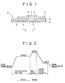
- FIG. 1 is a schematic cross-sectional view of a portion of a slide boat used in Example 1, described later, of the present invention; and
- FIG. 2 is a graph showing a correlation between the temperature and the time observed when Example 1 is achieved.
-
- The liquid-phase growth process of a compound semiconductor according to this invention is characterized in that the composition of a mixed gas atmosphere is changed immediately before the start of a liquid-phase growth to prevent generation of a surface defect in the form of either a large hole or a small hole.
- For instance, when an atmosphere consisting of 5:5 mixture of hydrogen and argon is used throughout a liquid-phase growth process, it is possible to prevent generation of a surface defect in the form of a large hole. However, the use of this mixed gas atmosphere is accompanied by generation of a surface defect in the form of a great number of small holes.
- On the other hand, when a 100% hydrogen atmosphere is used throughout the liquid-phase growth process, generation of a surface defect in the form of a small hole can be substantially prevented. However, a surface defect in the form of a large hole is generated.
- According to a feature of this invention, before the start of a liquid-phase growth, a substrate and a Ga melt are baked by a hydrogen gas atmosphere (100% hydrogen or a mixed gas consisting of more than 80% of hydrogen and the rest of an inert gas) to reduce the possibility of occurrence of a surface defect in the form of a small hole caused by contamination of the substrate and the Ga melt.
- Furthermore, according to another feature of this invention, immediately before the start of the liquid-phase growth, the existing gas atmosphere is replaced by a mixed gas consisting of not more than 50% hydrogen and the rest of the inert gas to reduce the generation of a surface defect in the form of a large hole caused by hydrogen gas bubbles.
- Thus, by changing the composition of the atmosphere before the start of the liquid-phase growth, it is possible to prevent generation of a surface defect either in the form of a large hole or in the form of a small hole.
- The invention will be further described by way of the following examples which should be construed as illustrative rather than restrictive.
- FIG. 1 shows a slide boat used to carry out the liquid-phase growth process of the invention. In FIG. 1, reference character S is a slide boat, 1 is a Ga melt, 2 is a receptacle, 3 is a cavity, 4 is a single crystal substrate, 5 is a recess, 6 is a GaP polycrystal, 11 is an upper slide plate, 12 is an intermediate slide plate and 13 is a lower slide plate.
- Using the slide boat S shown in FIG. 1, an n-type GaP epitaxial layer was grown on the
substrate 4 in the sequence described below. - (1) Insert the slide boat S into a reaction furnace
with a
Ga melt 1 and asingle crystal substrate 4 held on the slide boat S. - (2) While supplying a 100% hydrogen gas (H2) into
the reaction furnace, heat the reaction furnace up to 1000°C
and thereafter maintain the reaction furnace at the same
temperature for 90 minutes, thereby causing the GaP polycrystal
to melt down into the
Ga melt 1 or solution (polycrystal melting in FIG. 2). In this instance, by H2, thesingle crystal substrate 4 is cleaned and an oxide film on theGa melt 1 is removed. - (3) Move the
intermediate slide plate 12 in the direction of the arrow X until thecavity 3 is in registry with thesingle crystal substrate 4, so that theGa melt 1 is brought into contact with thesingle crystal substrate 4. - (4) Heat the reaction furnace up to 1010°C and hold the reaction furnace at this temperature for 30 minutes, thereby causing the single crystal substrate to melt back into the Ga melt 1 (melt back in FIG. 2).
- (5) Change 100% H2 to a mixed gas consisting of 50% of H2 and 50% of argon and then start cooling of the reaction furnace at the rate of 1 - 3°C per minute, thereby commencing a liquid phase growth of an epitaxial layer.
- (6) When the reaction furnace is cooled down to
700°C, move the
intermediate slide plate 12 in the direction of the arrow Y, thereby terminating the liquid-phase growth. - (7) Visually inspect the presence of a surface
defect in a surface of the thus obtained epitaxial layer on
the
substrate 4. -
- The visual inspection indicated that neither a surface defect in the form of a large hole nor a surface defect in the form of a small hole could be found out. Regarding both of the large-hole surface defect and the small-hole surface defect, the average generation rate was 0%.
- For better understanding of the foregoing sequence of the Example 1, a correlation between the temperature and the time is shown in FIG. 2.
- An n-type GaP epitaxial growth layer was produced by repeating the procedure of Example 1 except that throughout the process, an atmosphere consisting of 100% hydrogen was used. A visual inspection of the obtained epitaxial layer on the substrate revealed the generation of both a surface defect composed of a large hole and a surface defect composed of a small hole. The average generation rate was 3.8% about the large-hole surface defect and 5.4% about the small-hole surface defect.
- An n-type GaP epitaxial growth layer was produced by repeating the procedure of example 1 with the following exceptions. During a first period of 30 minutes of the step of polycrystal melting, an atmosphere consisting of 5:5 mixture of hydrogen and argon was used, and the rest (60 minutes) of the polycrystal melting step was carried out in a 100% hydrogen atmosphere. In addition, the melt back step and the liquid-phase growth step were carried out in an atmosphere consisting of 5:5 mixture of hydrogen and argon. A visual inspection of the obtained epitaxial substrate failed to find the generation of a large-hole surface defect but revealed a small-hole surface defect. The average generation rate was 0.0% about the large-hole surface defect and 41.5% about the small-hole surface defect.
- An n-type GaP epitaxial growth layer was produced by repeating the procedure of Example 1 with the exception that a first period of 30 minutes of the polycrystal melting step was carried out in an atmosphere consisting of 5:5 mixture of hydrogen and argon, and the rest (60 minutes) of the polycrystal melting step, the melt back step and the liquid-phase growth step were carried out in a 100% hydrogen atmosphere. A visual inspection of the obtained epitaxial substrate indicated that both a large-hole surface defect and a small-hole surface defect were induced. The average generation rate was 3.3% about the large-hole surface defect and 5.3% about the small-hole surface defect.
- An n-type GaP epitaxial growth layer was produced by repeating the procedure of Example 1 with the exception that the polycrystal melting step was carried out in a 100% hydrogen atmosphere, and the melt back step and the liquid-phase growth step were carried out in an atmosphere consisting of 5:5 mixture of hydrogen and argon. A visual inspection of the obtained epitaxial substrate traced the generation of a small-hole surface defect only. The average generation rate was 0.0% about the large-hole surface defect and 3.3% about the small-hole surface defect.
- In the examples described above, a melt back step is included, however, the present invention is also applicable to a liquid-phase growth process devoid of the melt back step.
- The liquid-phase growth process of this invention is carried out by the slide boat method, as described above. This is illustrative rather than restrictive and, hence, the present invention is also applicable to the tipping method and the dipping method.
- As described above, the liquid-phase growth process according to this invention is effective to prevent generation of a surface defect and improve the product quality and the production yield.
Claims (2)
- A liquid phase process for growing a III-V compound semiconductor comprising Ga, comprising the steps of:characterized in that:holding a single crystal substrate and a solution of a polycrystal in a Ga melt, in a first gas atmosphere consisting of either 100% hydrogen or of a mixture of more than 80% hydrogen and the rest of an inert gas; andstarting the liquid phase growth step after changing said first gas atmosphere to a second gas atmosphere,
said second gas atmosphere is a mixed gas atmosphere consisting of not more than 50% of hydrogen and the rest of said inert gas. - A liquid phase growth process according to claim 1, wherein said inert gas is argon.
Applications Claiming Priority (3)
| Application Number | Priority Date | Filing Date | Title |
|---|---|---|---|
| JP3212848A JP2503130B2 (en) | 1991-07-29 | 1991-07-29 | Liquid phase growth method |
| JP21284891 | 1991-07-29 | ||
| JP212848/91 | 1991-07-29 |
Publications (3)
| Publication Number | Publication Date |
|---|---|
| EP0525617A2 EP0525617A2 (en) | 1993-02-03 |
| EP0525617A3 EP0525617A3 (en) | 1995-10-11 |
| EP0525617B1 true EP0525617B1 (en) | 2001-01-31 |
Family
ID=16629332
Family Applications (1)
| Application Number | Title | Priority Date | Filing Date |
|---|---|---|---|
| EP92112538A Expired - Lifetime EP0525617B1 (en) | 1991-07-29 | 1992-07-22 | Liquid-phase growth process of compound semiconductor |
Country Status (4)
| Country | Link |
|---|---|
| US (1) | US5234534A (en) |
| EP (1) | EP0525617B1 (en) |
| JP (1) | JP2503130B2 (en) |
| DE (1) | DE69231670T2 (en) |
Families Citing this family (1)
| Publication number | Priority date | Publication date | Assignee | Title |
|---|---|---|---|---|
| JP4707203B2 (en) * | 1999-09-09 | 2011-06-22 | ローム株式会社 | Semiconductor device |
Family Cites Families (9)
| Publication number | Priority date | Publication date | Assignee | Title |
|---|---|---|---|---|
| JPS4921990B1 (en) * | 1969-07-23 | 1974-06-05 | ||
| US3933538A (en) * | 1972-01-18 | 1976-01-20 | Sumitomo Electric Industries, Ltd. | Method and apparatus for production of liquid phase epitaxial layers of semiconductors |
| US4110133A (en) * | 1976-04-29 | 1978-08-29 | The Post Office | Growth of semiconductor compounds by liquid phase epitaxy |
| JPS5567130A (en) * | 1978-11-14 | 1980-05-21 | Mitsubishi Electric Corp | Method of manufacturing semiconductor crystal |
| JPS5596629A (en) * | 1979-01-17 | 1980-07-23 | Matsushita Electric Ind Co Ltd | Method of epitaxially growing in liquid phase |
| US4263064A (en) * | 1980-02-19 | 1981-04-21 | The United States Of America As Represented By The Secretary Of The Navy | Method of liquid phase epitaxial growth |
| JPS593097A (en) * | 1982-06-25 | 1984-01-09 | Toshiba Corp | Liquid phase epitaxial growth method |
| US4500367A (en) * | 1983-10-31 | 1985-02-19 | At&T Bell Laboratories | LPE Growth on group III-V compound semiconductor substrates containing phosphorus |
| JPS60239397A (en) * | 1984-05-11 | 1985-11-28 | Showa Denko Kk | Preparation of red light emitting element comprising gallium phosphide |
-
1991
- 1991-07-29 JP JP3212848A patent/JP2503130B2/en not_active Expired - Fee Related
-
1992
- 1992-07-22 DE DE69231670T patent/DE69231670T2/en not_active Expired - Fee Related
- 1992-07-22 EP EP92112538A patent/EP0525617B1/en not_active Expired - Lifetime
- 1992-07-27 US US02/719,331 patent/US5234534A/en not_active Expired - Fee Related
Also Published As
| Publication number | Publication date |
|---|---|
| US5234534A (en) | 1993-08-10 |
| DE69231670D1 (en) | 2001-03-08 |
| EP0525617A2 (en) | 1993-02-03 |
| EP0525617A3 (en) | 1995-10-11 |
| DE69231670T2 (en) | 2001-06-07 |
| JPH0532481A (en) | 1993-02-09 |
| JP2503130B2 (en) | 1996-06-05 |
Similar Documents
| Publication | Publication Date | Title |
|---|---|---|
| JPH05500883A (en) | How to process silicon carbide surfaces for crystal growth | |
| US3729348A (en) | Method for the solution growth of more perfect semiconductor crystals | |
| US5234534A (en) | Liquid-phase growth process of compound semiconductor | |
| US4500367A (en) | LPE Growth on group III-V compound semiconductor substrates containing phosphorus | |
| US4261770A (en) | Process for producing epitaxial semiconductor material layers on monocrystalline substrates via liquid phase shift epitaxy | |
| US4255228A (en) | Method of growing quartz | |
| JPS626338B2 (en) | ||
| JPS5930797A (en) | Liquid phase epitaxial growth method | |
| JP4863264B2 (en) | Manufacturing method of semiconductor crystal | |
| JP3101753B2 (en) | Vapor growth method | |
| JPH0930891A (en) | Semiconductor liquid phase epitaxial device | |
| JPH0247440B2 (en) | ||
| US4371420A (en) | Method for controlling impurities in liquid phase epitaxial growth | |
| JPH03236219A (en) | Surface treating method for semiconductor substrate | |
| JPH0354185A (en) | Production of iii-v compound semiconductor single crystal | |
| JP2003146791A (en) | Method for producing compound semiconductor single crystal | |
| Tamari et al. | LPE growth of Pb1-xSnxTe layers on metal-etched substrates | |
| JPH03153596A (en) | Liquid phase epitaxial growth equipment | |
| JPS62241893A (en) | Liquid phase epitaxial growth method | |
| JPH01212297A (en) | Growth of iii-v group compound semiconductor crystal on si substrate | |
| JPH02102191A (en) | Growth of semiconductor crystal | |
| JPS6052578B2 (en) | Manufacturing method of semiconductor device | |
| Lessoff et al. | Research on Gunn Effect Materials (III-V Compounds) | |
| JPH04362082A (en) | Apparatus and method for producing compound semiconductor crystal | |
| JPS57103314A (en) | Method for liquid phase epitaxial growth |
Legal Events
| Date | Code | Title | Description |
|---|---|---|---|
| PUAI | Public reference made under article 153(3) epc to a published international application that has entered the european phase |
Free format text: ORIGINAL CODE: 0009012 |
|
| AK | Designated contracting states |
Kind code of ref document: A2 Designated state(s): DE FR GB |
|
| PUAL | Search report despatched |
Free format text: ORIGINAL CODE: 0009013 |
|
| RHK1 | Main classification (correction) |
Ipc: H01L 21/208 |
|
| AK | Designated contracting states |
Kind code of ref document: A3 Designated state(s): DE FR GB |
|
| 17P | Request for examination filed |
Effective date: 19951229 |
|
| 17Q | First examination report despatched |
Effective date: 19971017 |
|
| GRAG | Despatch of communication of intention to grant |
Free format text: ORIGINAL CODE: EPIDOS AGRA |
|
| GRAG | Despatch of communication of intention to grant |
Free format text: ORIGINAL CODE: EPIDOS AGRA |
|
| GRAH | Despatch of communication of intention to grant a patent |
Free format text: ORIGINAL CODE: EPIDOS IGRA |
|
| GRAH | Despatch of communication of intention to grant a patent |
Free format text: ORIGINAL CODE: EPIDOS IGRA |
|
| GRAA | (expected) grant |
Free format text: ORIGINAL CODE: 0009210 |
|
| AK | Designated contracting states |
Kind code of ref document: B1 Designated state(s): DE FR GB |
|
| PG25 | Lapsed in a contracting state [announced via postgrant information from national office to epo] |
Ref country code: FR Free format text: LAPSE BECAUSE OF FAILURE TO SUBMIT A TRANSLATION OF THE DESCRIPTION OR TO PAY THE FEE WITHIN THE PRESCRIBED TIME-LIMIT Effective date: 20010131 |
|
| REF | Corresponds to: |
Ref document number: 69231670 Country of ref document: DE Date of ref document: 20010308 |
|
| EN | Fr: translation not filed | ||
| PG25 | Lapsed in a contracting state [announced via postgrant information from national office to epo] |
Ref country code: GB Free format text: LAPSE BECAUSE OF NON-PAYMENT OF DUE FEES Effective date: 20010722 |
|
| PLBE | No opposition filed within time limit |
Free format text: ORIGINAL CODE: 0009261 |
|
| STAA | Information on the status of an ep patent application or granted ep patent |
Free format text: STATUS: NO OPPOSITION FILED WITHIN TIME LIMIT |
|
| 26N | No opposition filed | ||
| GBPC | Gb: european patent ceased through non-payment of renewal fee |
Effective date: 20010722 |
|
| PGFP | Annual fee paid to national office [announced via postgrant information from national office to epo] |
Ref country code: DE Payment date: 20020731 Year of fee payment: 11 |
|
| PG25 | Lapsed in a contracting state [announced via postgrant information from national office to epo] |
Ref country code: DE Free format text: LAPSE BECAUSE OF NON-PAYMENT OF DUE FEES Effective date: 20040203 |