EP0520105B1 - Nacelle pour plaquettes semiconductrices - Google Patents
Nacelle pour plaquettes semiconductrices Download PDFInfo
- Publication number
- EP0520105B1 EP0520105B1 EP91305897A EP91305897A EP0520105B1 EP 0520105 B1 EP0520105 B1 EP 0520105B1 EP 91305897 A EP91305897 A EP 91305897A EP 91305897 A EP91305897 A EP 91305897A EP 0520105 B1 EP0520105 B1 EP 0520105B1
- Authority
- EP
- European Patent Office
- Prior art keywords
- side walls
- wafer
- ribs
- walls
- stay means
- Prior art date
- Legal status (The legal status is an assumption and is not a legal conclusion. Google has not performed a legal analysis and makes no representation as to the accuracy of the status listed.)
- Expired - Lifetime
Links
Images


Classifications
-
- H—ELECTRICITY
- H10—SEMICONDUCTOR DEVICES; ELECTRIC SOLID-STATE DEVICES NOT OTHERWISE PROVIDED FOR
- H10P—GENERIC PROCESSES OR APPARATUS FOR THE MANUFACTURE OR TREATMENT OF DEVICES COVERED BY CLASS H10
- H10P72/00—Handling or holding of wafers, substrates or devices during manufacture or treatment thereof
- H10P72/10—Handling or holding of wafers, substrates or devices during manufacture or treatment thereof using carriers specially adapted therefor, e.g. front opening unified pods [FOUP]
- H10P72/15—Horizontal carrier comprising wall type elements whereby the substrates are vertically supported, e.g. comprising sidewalls
Definitions
- the present invention relates to a wafer basket for holding, cleaning, drying, storing and transporting a large number of semiconductor wafers. More particularly, the invention relates to a wafer basket which is designed to improve cleaning and drying conditions for the wafers held in it.
- a wafer basket is a box-like rack for containing semiconductor wafers, and is commonly molded integrally of PFA (a copolymer synthesized from perfluoroalkylvinyl ether and tetrafluoroethylene), which is an excellent material in chemical resistance and heat resistance.
- PFA a copolymer synthesized from perfluoroalkylvinyl ether and tetrafluoroethylene
- the wafer basket comprises numerous shelves for receiving wafers in a row, each shelf consisting of a groove defined by a pair of neighboring partition ribs which ribs are formed at regular intervals.
- the wafer basket is also a vehicle means for transporting the wafers it contains.
- a typical conventional wafer basket is described as follows. Being box-like, a wafer basket has four walls, of which two are called side walls. The other two walls parallel to each other are called a front wall and a rear wall, respectively. The side walls are also parallel to each other except for the lower portions where they are bent and curved inwardly in a manner such that a wafer-sized circle may be roughly inscribed to the inner surfaces of the side walls.
- the inner surfaces of the side walls are formed with vertical partition ribs in a manner such that the ribs formed on one side wall are in mirror symmetry with those formed on the other side wall, and such that each pair of neighboring partition ribs on one side wall cooperate with that pair on the other side wall in mirror-symmetric relation to the former to define a groove within themselves suitable for receiving the edge portion of a wafer, and the wafers thus received are constrained to stand at regular intervals and parallel to the front and rear walls.
- Slit holes are made along the grooves in either side wall such that the slit holes render the grooves bottomless where the slits are made. These slits provide passages for the treating liquid to enter the wafer basket when the basket is steeped in the treating liquid.
- the wafer basket has no ceiling or bottom floor, but the lower bent portions of the side walls provide a support means so that the wafers do not fall through the wafer basket.
- each groove in the bent portions of the side walls holds the wafer between the ribs, and the wafer received fits therein in a manner such that considerable portions of the edge of the wafer which are inside the grooves formed in the curved lower portions of the side walls are in contact with the bottoms or the side slopes of the grooves between the ribs.
- the downward movement of the wafers is checked by the ribs.
- the conventional wafer basket is provided with four recesses each at the four top corners, that is, at either top lateral end of the side walls.
- the recesses are formed in a shape such that they can engage with the hooks of a basket lifter.
- the wafer basket is lifted, transported, steeped in a treatment liquid or a cleaning liquid, and suspended in the air for various treatments.
- the grooves formed in the lower portions of the side walls are formed in a manner such that the diameter of the circular arcs traced by each curved groove is roughly identical to the diameter of the wafer to be received [ref., for example, Japanese Published Patent Kokoku No.
- the lengthy slits cut through the groove bottoms provide passages for a liquid to enter the wafer basket when the wafer basket loaded with wafers is steeped in a cleaning liquid or etching liquid during the wafer cleaning operation or wafer etching operation, as well as passages for the liquid to drain when the basket is lifted above the liquid.
- the slit holes are relatively narrow and the peripheral edges of the wafers nearly plug them, the liquid does not pass through them freely, and when the basket is lifted above the liquid, some liquid tends to be held in the slit holes owing to the capillary phenomenon, so that the basket gets rid of the liquid poorly, and during the vapor drying operation the remnant liquid leaves stains and particles at the edge of the wafer and prevents proper drying thereof.
- This invention was invented in view of the foregoing circumstances, and it is an object of the invention to provide a wafer basket which is constructed simply and functionally such that a fluid can pass the wafer basket freely and the wafers contained therein are secure from the problems of poor cleaning and drying and thus are free from stains, and also that the weight and cost of the basket are significantly reduced.
- a wafer basket was newly designed.
- the wafer basket is molded integrally of a resin such as PFA like the conventional wafer baskets, it differs from the conventional wafer baskets shown in US-A-4 471 716 in the features of the characterising part of claim 1.
- the dented stay means having semicircular cross section at their upper edges are provided to support the wafers, the wafers mounted on the stay means are virtually in point-wise contact with the stay means, and furthermore, since the vacancies of considerable size are formed where the bent portions of the side walls are removed, considerable lengths of the wafer edges do not have to touch any part of the wafer basket. Consequently, the edges of the wafers are cleaned well during the cleaning operations, and the cleaning liquid scarcely stays on the wafers when the wafer basket is lifted from the cleaning liquid so that no stains are formed during the vapor drying operation. As a result, the wafers are dried properly and are not contaminated with particles so that the yield of the semiconductor chips obtained from the wafers is improved and the reliability of the product quality becomes higher.
- the fluid can pass the wafer basket freely, and, thus, when the wafer basket is lifted above the liquid, the wafer basket can get rid of the liquid quickly with the result that the wafers contained therein are secure from the problems of poor cleaning and drying, and thus are free from stains. Since the present wafer basket is simpler, the consumption of the material (PFA) is reduced and thus the weight and cost of the basket are significantly reduced.
- PFA material
- a wafer basket 1 according to the present invention has side walls 2-1 and 2-2 opposed to and parallel to each other, and a front wall 3-1 and a rear wall 3-2 which are also opposed to and parallel to each other and are integrally formed with the side walls 2-1 and 2-2 to which they are connected normally at the lateral edges. These four walls thus give the wafer basket 1 a box-like configuration; but the wafer basket 1 does not have a ceiling or a floor.
- the wafer basket 1 is molded integrally of PFA, a fluorine-containing resin, like the conventional wafer baskets.
- the upper and lower portions of the front wall 3-1 and the rear wall 3-2 are substantially removed in a manner such that the remnants of the front and the rear walls look like a letter "H" (ref. Fig. 1).
- a pair of stiffening ribs 4, 4 are provided across the outer face of the front wall 3-1, and, as shown in Fig. 3 in addition to Figs. 4 and 5, an indexing protrusion 5 in the shape of a half cylinder extending in the direction of the width of the front wall 3-1 is formed in the middle of the generally rectangular portion of the front wall 3-1 which is bounded by the stiffening ribs 4, 4.
- the side walls 2-1 and 2-2 are provided with flanges 2a-1 and 2a-2, respectively, which extend horizontally outward from the upper edges of the side walls.
- a small circular bore 6 is provided at either end of the flange 2a-1, for positioning the wafer basket 1.
- the other flange 2a-2 is provided with a small round-topped protrusion 7 at either end thereof.
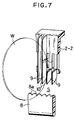
- the side walls 2-1 and 2-2 each have a pair of strip-like extensions 2A, 2B which extend from the lower corners of the walls and are bent inwardly in a manner such that a wafer-sized circle may be roughly inscribed to the inner surfaces of the side walls 2-1, 2-2 and the bent extensions 2A, 2B.
- a plate-like stay 8 is provided at the lower ends of either pair of the extensions 2A, 2B, in a manner such that each stay 8 is passed in the direction normal to the front and rear walls 3-1, 3-2, and extends from the front wall 3-1 to the rear wall 3-2. As shown in Figs.
- a space S is defined by the stay 8, the lower edge of the side wall 2-1 or 2-2, and the pair of extensions 2A, 2B on either side of the wafer basket 1.
- the extensions 2A, 2B can also be considered as flanges extending normally from the front and rear walls, respectively, and the manner of drafting the claims will regard the extensions 2A, 2B as such.
- the vacancy S can also be said to be defined by the stay 8, the lower edge of the side wall, and the lower portions of the front and rear walls.
- the inner surface of either of the vertical side walls 2-1, 2-2 is formed with wafer-partition ribs 9 each extending vertically from the top of the side wall to a point substantially beyond the lower edge of the side wall.
- the lower end of each rib is shaped like a knife edge, and disposed in the vacancy S.
- the ribs 9 (nineteen ribs in this embodiment, as seen in Fig. 4) are arranged in a row at regular intervals from the front wall 3-1 to the rear wall 3-2; and the ribs formed on the side wall 2-1 are in mirror symmetry with the ribs formed on the side wall 2-2.
- Each pair of neighboring ribs 9, 9 define a groove 10 having a width suitable for receiving in it the edge portion of a wafer W.
- the grooves formed on the side wall 2-1 are mirror-symmetric with those formed on the side wall 2-2, so that a wafer W can be received in each pair of opposing grooves.
- the foremost and the rearmost ribs define similar grooves in cooperation with the partitionable risings raised from the inside surfaces of the side walls, so that the wafer basket 1 can hold twenty wafers at a time in a manner such that the wafers are arranged between the front and rear walls at regular intervals.
- the upper edges of the stays 8, 8 are formed with numerous indents 8a at the same regular intervals as the grooves 10 of the side wall are formed so that a wafer received in a certain groove and in the corresponding indent is constrained to stand in parallel to the front and rear walls.
- the upper edges of the dented stay means 8, 8 are roughly semicircular when seen in their cross section cut by a plane parallel to the front wall and passing through an indent between any dents, as shown in Fig. 2.
- Slit holes 11 are made in the vertical side walls 2-1 and 2-2 such that the slit holes 11 render the grooves 10 bottomless where the slits are made.
- the slit 11 has a slanted upper end face 11a and a slanted lower end face 11b such that it has a profile of diverging externally.
- the vacancy S has a slanted upper end face Sa, so that it also diverges externally.
- the wafers W are put into the wafer basket 1 by letting them slide down into the grooves 10 formed in the side walls 2-1, 2-2, from above. This downward movement of a wafer W is checked by the stays 8 when the wafer W is received in a dent and mounted on the stays 8. In this manner twenty wafers W are contained in a row in the wafer basket 1, and they are all isolated from the neighboring ones by the partitioning ribs 9.
- each wafer W is only contacted by the stays 8 and by the ribs 9.
- the area of the contact is virtually a point a each.
- the wafer W is mounted on the stays 8, and the existence of the vacancies S enables substantial portions of the wafer edge to avoid contacting the wafer basket, the contact between the wafer W and the ribs 9 are scanty and temporal. Also, the vacancies S allow quick draining of the wafer basket.
Landscapes
- Packaging Frangible Articles (AREA)
- Container, Conveyance, Adherence, Positioning, Of Wafer (AREA)
Claims (2)
- Nacelle pour plaquettes semi-conductrices comprenant :
deux parois latérales (2-1, 2-2) agencées en vis-à-vis et parallèlement l'une à l'autre, présentant sur leurs faces internes respectives une pluralité de nervures verticales (9) agencées à des intervalles réguliers en vue de définir des rainures (10) destinées à recevoir des plaquettes semi-conductrices, les rainures (10) ménagées sur l'une des parois latérales (2-1) et les rainures (10) ménagées sur l'autre paroi latérale (2-2) étant disposées symétriquement par rapport à un plan ;
une paroi antérieure (3-1) et une paroi postérieure (3-2) agencées en vis-à-vis, parallèlement l'une à l'autre et perpendiculairement aux parois latérales (2-1, 2-2), les parois latérales (2-1, 2-2) s'étendant et étant maintenues entre lesdites parois antérieure et postérieure (3-1, 3-2) ;
deux moyens de support (8) parallèles, s'étendant et étant maintenus entre lesdites parois antérieure et postérieure (3-1, 3-2) à une position sensiblement plus basse que les bords inférieurs des parois latérales (2-1, 2-2) et étant sensiblement plus proches l'un de l'autre que les bords inférieurs des parois latérales (2-1, 2-2), lesdites parois latérales (2-1, 2-2) et lesdits moyens de support (8) étant configurés de telle sorte qu'un cercle de la taille d'une plaquette semi-conductrice puisse s'inscrire approximativement dans les côtés internes des parois latérales (2-1, 2-2) et les surfaces supérieures des moyens de support (8), une plaquette semi-conductrice (W) logée dans une paire de rainures correspondantes (10) des parois latérales (2-1, 2-2) reposant sur lesdits moyens de support (8) et étant maintenue sensiblement parallèlement aux parois antérieure et postérieure (3-1, 3-2) ;
les bords inférieurs des parois latérales (2-1, 2-2), les parties inférieures des parois antérieure et postérieure (3-1, 3-2) et les moyens de support (8) définissant ensemble des ouvertures de vidange (S) relativement grandes ; caractérisée en ce que :
chaque moyen de support (8) présente sur sa face supérieure une pluralité d'entailles (8a) ménagées selon les mêmes intervalles réguliers que les rainures (10) définies entre les nervures (9) des parois latérales (2-1, 2-2), de telle sorte que ladite plaquette semi-conductrice (W) logée dans une paire de rainures correspondantes (10) des parois latérales (2-1, 2-2) repose dans une paire d'entailles (8a) correspondantes, ménagées sur lesdits moyens de support (8) ; en ce que
les surfaces supérieures des moyens de support (8), dans lesquels sont pratiquées les entailles, présentent, lorsqu'elles sont vues en coupe selon un plan parallèle à ladite paroi antérieure (3-1), un profil incurvé et sont en contact essentiellement ponctuel (a) avec ladite plaquette semi-conductrice (W) ; en ce que :
lesdites nervures (9) s'étendent vers le bas au-delà des bords inférieurs desdites parois latérales (2-1, 2-2) pour aboutir dans les ouvertures (S), entre les bords inférieurs desdites parois latérales (2-1, 2-2) et les bords supérieurs desdits moyens de support (8), les parties des nervures (9) dépassant au-dessous des bords inférieurs des parois latérales (2-1, 2-2) étant conformées de façon à être comprises dans la périphérie latérale de la nacelle, définie par les parois antérieure et postérieure (3-1, 3-2), et les extrémités inférieures desdites nervures (9) étant biseautées, vues dans une direction normale auxdites parois latérales (2-1, 2-2) ; en ce que :
lesdites parois latérales (2-1, 2-2) comportant également une pluralité de fentes verticales (11) pratiquées dans chacune desdites rainures (10) définies par lesdites nervures (9) ; et en ce que :
les faces (11a, 11b, Sa), définies par les extrémités verticales supérieures et inférieures desdites fentes (11) et le bord inférieur desdites parois latérales (2-1, 2-2), sont inclinées par rapport auxdites parois latérales (2-1, 2-2). - Nacelle pour plaquettes semi-conductrices selon la revendication 1, caractérisée en ce que lesdites ouvertures (S) sont définies par les extrémités inférieures des parois latérales (2-1, 2-2), les brides (2A, 2B) s'étendant perpendiculairement depuis les parties inférieures des parois antérieure et postérieure (3-1, 3-2) et les moyens de support (8).
Priority Applications (2)
| Application Number | Priority Date | Filing Date | Title |
|---|---|---|---|
| EP91305897A EP0520105B1 (fr) | 1991-06-28 | 1991-06-28 | Nacelle pour plaquettes semiconductrices |
| DE69112613T DE69112613T2 (de) | 1991-06-28 | 1991-06-28 | Trägerkassette für Halbleiterscheiben. |
Applications Claiming Priority (1)
| Application Number | Priority Date | Filing Date | Title |
|---|---|---|---|
| EP91305897A EP0520105B1 (fr) | 1991-06-28 | 1991-06-28 | Nacelle pour plaquettes semiconductrices |
Publications (2)
| Publication Number | Publication Date |
|---|---|
| EP0520105A1 EP0520105A1 (fr) | 1992-12-30 |
| EP0520105B1 true EP0520105B1 (fr) | 1995-08-30 |
Family
ID=8208327
Family Applications (1)
| Application Number | Title | Priority Date | Filing Date |
|---|---|---|---|
| EP91305897A Expired - Lifetime EP0520105B1 (fr) | 1991-06-28 | 1991-06-28 | Nacelle pour plaquettes semiconductrices |
Country Status (2)
| Country | Link |
|---|---|
| EP (1) | EP0520105B1 (fr) |
| DE (1) | DE69112613T2 (fr) |
Cited By (1)
| Publication number | Priority date | Publication date | Assignee | Title |
|---|---|---|---|---|
| CN104465463A (zh) * | 2014-12-16 | 2015-03-25 | 中国电子科技集团公司第四十六研究所 | 一种承托多个尺寸硅外延片的花篮结构 |
Families Citing this family (2)
| Publication number | Priority date | Publication date | Assignee | Title |
|---|---|---|---|---|
| TW296361B (fr) * | 1995-06-26 | 1997-01-21 | Kakizaki Seisakusho Kk | |
| CN112582315B (zh) * | 2021-03-01 | 2021-05-07 | 常州江苏大学工程技术研究院 | 一种防氧化硅片清洗装置 |
Family Cites Families (2)
| Publication number | Priority date | Publication date | Assignee | Title |
|---|---|---|---|---|
| US4471716A (en) * | 1981-01-15 | 1984-09-18 | Fluoroware, Inc. | Wafer carrier |
| WO1989000333A1 (fr) * | 1987-07-02 | 1989-01-12 | Fluoroware, Inc. | Support renforce avec piece rigide encastree |
-
1991
- 1991-06-28 DE DE69112613T patent/DE69112613T2/de not_active Expired - Fee Related
- 1991-06-28 EP EP91305897A patent/EP0520105B1/fr not_active Expired - Lifetime
Cited By (1)
| Publication number | Priority date | Publication date | Assignee | Title |
|---|---|---|---|---|
| CN104465463A (zh) * | 2014-12-16 | 2015-03-25 | 中国电子科技集团公司第四十六研究所 | 一种承托多个尺寸硅外延片的花篮结构 |
Also Published As
| Publication number | Publication date |
|---|---|
| EP0520105A1 (fr) | 1992-12-30 |
| DE69112613T2 (de) | 1996-05-02 |
| DE69112613D1 (de) | 1995-10-05 |
Similar Documents
| Publication | Publication Date | Title |
|---|---|---|
| US4471716A (en) | Wafer carrier | |
| EP0520106B1 (fr) | Nacelle pour plaquettes semiconductrices | |
| US4339051A (en) | Silverware basket | |
| EP0530332B1 (fr) | Couvercle amortissant de receptacle contenant des tranches de circuits integres | |
| US8353412B2 (en) | Insert for a dish basket for an automatic dishwasher | |
| US3923156A (en) | Wafer basket | |
| US4724963A (en) | Wafer processing cassette | |
| US3486631A (en) | Basket for polished wafers | |
| US5086544A (en) | Cutlery basket for dish-washing machine | |
| US20060216942A1 (en) | Wafer carrier for minimizing contacting area with wafers | |
| TW201628118A (zh) | 具有單一出口流方向的緩衝器站 | |
| US3000528A (en) | Egg tray | |
| US8746260B2 (en) | System and method for cleaning tokens | |
| EP0520105B1 (fr) | Nacelle pour plaquettes semiconductrices | |
| US5429251A (en) | Semiconductor wafer end effector | |
| NZ280605A (en) | Dish draining rack with an inwardly opening, vertical depression in at least one of the side wall panels | |
| US3383148A (en) | Protective device for dishwasher door | |
| US3394819A (en) | Article supporting device | |
| US5485861A (en) | Cleaning tank | |
| US7621287B2 (en) | Arrangement for improving the drying performance of an automatic dishwasher | |
| KR100738122B1 (ko) | 웨이퍼 등의 정밀 기판 수용 용기 | |
| US6868977B2 (en) | Adapter for a dish basket of a dishwasher | |
| US5878889A (en) | Semiconductor wafer carrier featuring effective reduction of airborne particles become attached to wafers | |
| JP3307652B2 (ja) | 基板を処理するための装置 | |
| US5573680A (en) | Method for etching a semiconductor material without altering flow pattern defect distribution |
Legal Events
| Date | Code | Title | Description |
|---|---|---|---|
| PUAI | Public reference made under article 153(3) epc to a published international application that has entered the european phase |
Free format text: ORIGINAL CODE: 0009012 |
|
| 17P | Request for examination filed |
Effective date: 19920518 |
|
| AK | Designated contracting states |
Kind code of ref document: A1 Designated state(s): DE FR GB |
|
| 17Q | First examination report despatched |
Effective date: 19930916 |
|
| GRAA | (expected) grant |
Free format text: ORIGINAL CODE: 0009210 |
|
| AK | Designated contracting states |
Kind code of ref document: B1 Designated state(s): DE FR GB |
|
| ET | Fr: translation filed | ||
| REF | Corresponds to: |
Ref document number: 69112613 Country of ref document: DE Date of ref document: 19951005 |
|
| PLBE | No opposition filed within time limit |
Free format text: ORIGINAL CODE: 0009261 |
|
| STAA | Information on the status of an ep patent application or granted ep patent |
Free format text: STATUS: NO OPPOSITION FILED WITHIN TIME LIMIT |
|
| 26N | No opposition filed | ||
| PGFP | Annual fee paid to national office [announced via postgrant information from national office to epo] |
Ref country code: FR Payment date: 19990610 Year of fee payment: 9 |
|
| PGFP | Annual fee paid to national office [announced via postgrant information from national office to epo] |
Ref country code: GB Payment date: 19990623 Year of fee payment: 9 |
|
| PGFP | Annual fee paid to national office [announced via postgrant information from national office to epo] |
Ref country code: DE Payment date: 19990626 Year of fee payment: 9 |
|
| PG25 | Lapsed in a contracting state [announced via postgrant information from national office to epo] |
Ref country code: GB Free format text: LAPSE BECAUSE OF NON-PAYMENT OF DUE FEES Effective date: 20000628 |
|
| GBPC | Gb: european patent ceased through non-payment of renewal fee |
Effective date: 20000628 |
|
| PG25 | Lapsed in a contracting state [announced via postgrant information from national office to epo] |
Ref country code: FR Free format text: LAPSE BECAUSE OF NON-PAYMENT OF DUE FEES Effective date: 20010228 |
|
| REG | Reference to a national code |
Ref country code: FR Ref legal event code: ST |
|
| PG25 | Lapsed in a contracting state [announced via postgrant information from national office to epo] |
Ref country code: DE Free format text: LAPSE BECAUSE OF NON-PAYMENT OF DUE FEES Effective date: 20010403 |