EP0519729B1 - Magnetic head driving circuit - Google Patents
Magnetic head driving circuit Download PDFInfo
- Publication number
- EP0519729B1 EP0519729B1 EP92305631A EP92305631A EP0519729B1 EP 0519729 B1 EP0519729 B1 EP 0519729B1 EP 92305631 A EP92305631 A EP 92305631A EP 92305631 A EP92305631 A EP 92305631A EP 0519729 B1 EP0519729 B1 EP 0519729B1
- Authority
- EP
- European Patent Office
- Prior art keywords
- magnetic head
- current
- coil
- auxiliary
- driving circuit
- Prior art date
- Legal status (The legal status is an assumption and is not a legal conclusion. Google has not performed a legal analysis and makes no representation as to the accuracy of the status listed.)
- Expired - Lifetime
Links
Images


Classifications
-
- G—PHYSICS
- G11—INFORMATION STORAGE
- G11B—INFORMATION STORAGE BASED ON RELATIVE MOVEMENT BETWEEN RECORD CARRIER AND TRANSDUCER
- G11B11/00—Recording on or reproducing from the same record carrier wherein for these two operations the methods are covered by different main groups of groups G11B3/00 - G11B7/00 or by different subgroups of group G11B9/00; Record carriers therefor
- G11B11/10—Recording on or reproducing from the same record carrier wherein for these two operations the methods are covered by different main groups of groups G11B3/00 - G11B7/00 or by different subgroups of group G11B9/00; Record carriers therefor using recording by magnetic means or other means for magnetisation or demagnetisation of a record carrier, e.g. light induced spin magnetisation; Demagnetisation by thermal or stress means in the presence or not of an orienting magnetic field
- G11B11/105—Recording on or reproducing from the same record carrier wherein for these two operations the methods are covered by different main groups of groups G11B3/00 - G11B7/00 or by different subgroups of group G11B9/00; Record carriers therefor using recording by magnetic means or other means for magnetisation or demagnetisation of a record carrier, e.g. light induced spin magnetisation; Demagnetisation by thermal or stress means in the presence or not of an orienting magnetic field using a beam of light or a magnetic field for recording by change of magnetisation and a beam of light for reproducing, i.e. magneto-optical, e.g. light-induced thermomagnetic recording, spin magnetisation recording, Kerr or Faraday effect reproducing
- G11B11/10502—Recording on or reproducing from the same record carrier wherein for these two operations the methods are covered by different main groups of groups G11B3/00 - G11B7/00 or by different subgroups of group G11B9/00; Record carriers therefor using recording by magnetic means or other means for magnetisation or demagnetisation of a record carrier, e.g. light induced spin magnetisation; Demagnetisation by thermal or stress means in the presence or not of an orienting magnetic field using a beam of light or a magnetic field for recording by change of magnetisation and a beam of light for reproducing, i.e. magneto-optical, e.g. light-induced thermomagnetic recording, spin magnetisation recording, Kerr or Faraday effect reproducing characterised by the transducing operation to be executed
- G11B11/1053—Recording on or reproducing from the same record carrier wherein for these two operations the methods are covered by different main groups of groups G11B3/00 - G11B7/00 or by different subgroups of group G11B9/00; Record carriers therefor using recording by magnetic means or other means for magnetisation or demagnetisation of a record carrier, e.g. light induced spin magnetisation; Demagnetisation by thermal or stress means in the presence or not of an orienting magnetic field using a beam of light or a magnetic field for recording by change of magnetisation and a beam of light for reproducing, i.e. magneto-optical, e.g. light-induced thermomagnetic recording, spin magnetisation recording, Kerr or Faraday effect reproducing characterised by the transducing operation to be executed to compensate for the magnetic domain drift or time shift
-
- G—PHYSICS
- G11—INFORMATION STORAGE
- G11B—INFORMATION STORAGE BASED ON RELATIVE MOVEMENT BETWEEN RECORD CARRIER AND TRANSDUCER
- G11B11/00—Recording on or reproducing from the same record carrier wherein for these two operations the methods are covered by different main groups of groups G11B3/00 - G11B7/00 or by different subgroups of group G11B9/00; Record carriers therefor
- G11B11/10—Recording on or reproducing from the same record carrier wherein for these two operations the methods are covered by different main groups of groups G11B3/00 - G11B7/00 or by different subgroups of group G11B9/00; Record carriers therefor using recording by magnetic means or other means for magnetisation or demagnetisation of a record carrier, e.g. light induced spin magnetisation; Demagnetisation by thermal or stress means in the presence or not of an orienting magnetic field
- G11B11/105—Recording on or reproducing from the same record carrier wherein for these two operations the methods are covered by different main groups of groups G11B3/00 - G11B7/00 or by different subgroups of group G11B9/00; Record carriers therefor using recording by magnetic means or other means for magnetisation or demagnetisation of a record carrier, e.g. light induced spin magnetisation; Demagnetisation by thermal or stress means in the presence or not of an orienting magnetic field using a beam of light or a magnetic field for recording by change of magnetisation and a beam of light for reproducing, i.e. magneto-optical, e.g. light-induced thermomagnetic recording, spin magnetisation recording, Kerr or Faraday effect reproducing
- G11B11/10502—Recording on or reproducing from the same record carrier wherein for these two operations the methods are covered by different main groups of groups G11B3/00 - G11B7/00 or by different subgroups of group G11B9/00; Record carriers therefor using recording by magnetic means or other means for magnetisation or demagnetisation of a record carrier, e.g. light induced spin magnetisation; Demagnetisation by thermal or stress means in the presence or not of an orienting magnetic field using a beam of light or a magnetic field for recording by change of magnetisation and a beam of light for reproducing, i.e. magneto-optical, e.g. light-induced thermomagnetic recording, spin magnetisation recording, Kerr or Faraday effect reproducing characterised by the transducing operation to be executed
- G11B11/10504—Recording
- G11B11/10508—Recording by modulating only the magnetic field at the transducer
Definitions
- the present invention relates to magnetic head driving circuits for driving a magnetic head for recording data on a recording medium, and more particularly, to a magnetic head driving circuit capable of over-writing data on a so-called magneto-optical disc.
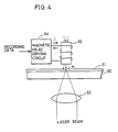
- Fig. 4 is a block diagram explaining the principle of such magneto-optical disc apparatus.
- the magneto-optical disc apparatus shown in Fig. 4 comprises a magneto-optical disc 50 having a vertical magnetization film 51, a lens 52 for picking up a laser beam, a magnetic head 53 and a magnetic head driving circuit 54.
- the lens 52 narrows down a laser beam and directs the same to the vertical magnetization film 51 of the magneto-optical disc 50.
- the irradiation of the laser beam causes the temperature of the vertical magnetization film 51 to exceed a Curie point.
- the magnetic head driving circuit 54 generates a drive current I in response to input data and supplies the current I to the magnetic head 53.
- the magnetic head 53 generates a magnetic field H in response to the supplied current I.
- the generated magnetic field is applied to the portion whose temperature exceeds the Curie point.
- a magnetic pattern corresponding to the input data is recorded on the magneto-optical disc 50.
- a magnetic head circuit for resolving such problem is disclosed in Japanese Patent Laying-Open No. 63-94406.
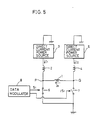
- Fig. 5 is a circuit diagram showing the magnetic head driving circuit described in Japanese Patent Laying-Open No. 63-94406.
- the magnetic head driving circuit comprises a magnetic head coil 1 having an impedance Lx, auxiliary coils 2 and 4, direct current power sources 3 and 5, switching devices 6 and 7, and a data modulator 8 for modulating input data (recording data) on a predetermined system to generate complementary recording signals S1, S1 ⁇ .
- the auxiliary coil 2 is connected between a node P which is one end of the magnetic head coil 1, and the direct current power source 3.
- the auxiliary coil 5 is connected between a node Q which is the other end of the magnetic head coil 1, and the direct current power source 5.
- Each of the auxiliary coils 2 and 4 has an impedance Ld (Ld >> Lx) larger than the impedance Lx of the magnetic head coil 1.
- the switching device 6 is connected between the node P and a ground terminal GND and is turned on/off in response to the recording signal S1.
- the switching device 7 is connected between the node Q and the ground terminal GND and is turned on/off in response to the recording signal S1 ⁇ .
- Fig. 6 is a diagram showing operation of the magnetic head driving circuit shown in Fig. 5.
- (a) is a waveform diagram of the recording signal S1
- (b) a waveform diagram of the recording signal S1 ⁇
- (c) a waveform diagram of the charging current I 1 flowing through the auxiliary coil 2
- (d) a waveform diagram of the charging current I 2 flowing through the auxiliary coil 4
- (e) a waveform diagram of the drive current Ix flowing through the magnetic head coil 1
- (f) shows a load impedance of the auxiliary coil 4
- (g) shows a load impedance of the auxiliary coil 2.
- the data modulator 8 modulates recording data to generate two recording signals S1 and S1 ⁇ complementary to each other.
- the recording signal S1 is applied to the switching device 6, while the recording signal S1 ⁇ is applied to the switching device 7.
- the switching device 6 is turned on in response to the recording signal S1 (logical high level) and the switching device 7 is turned off in response to the recording signal S1 ⁇ (logical low level)
- the circuit shown by the solid line in Fig. 5 is established wherein the charging current I 1 for charging the auxiliary coil 2 flows from the direct current power source 3 to the ground terminal GND through the auxiliary coil 2 and the switching device 6.
- the charging current I 2 for charging the auxiliary coil 4 flows from the direct current power source 5 to the ground terminal GND through the auxiliary coil 4, the magnetic head coil 1 and the switching device 6.
- the magnetic head coil 1 is supplied with the drive current I X from the node Q toward the node P.
- the charging current I 2 for charging the auxiliary coil 4 flows from the direct current power source 5 to the ground terminal GND through the auxiliary coil 4 and the switching device 7.
- the charging current I 1 for charging the auxiliary coil 2 flows from the direct current power source 3 to the ground terminal GND through the auxiliary coil 2, the magnetic head coil 1 and the switching device 7.
- the drive current I X therefore flows to the magnetic head coil 1 from the node P toward the node Q.
- the load of the auxiliary coil 2 (see Fig. 6 (g)) and the load of the auxiliary coil 4 (see Fig. 6 (f)) attain the impedance Lx of the magnetic head coil or 0.
- the above-mentioned impedance Ld should be as small as possible. As the impedance Ld is decreased, Lx becomes so relatively large that it is not negligible with respect to Ld. In other words, load fluctuation occurs.
- the above-described problem becomes particularly conspicuous in the following case. That is, it is a case where a generally known and employed NRZI recording system (Non-return to Zero Inverse) of 2-7 RLL code (2-7 Run Length Limited) is used as modulation system for recording/reproduction in a magneto-optical disc apparatus. While such system has an advantage of increasing a recording density, it also has a disadvantage that a recording signal which recording bits are modulated includes a large amount of direct current components. It is therefore impossible to avoid the above-described problem when a recording signal of the above-described system is input to a conventional magnetic head driving circuit.
- NRZI recording system Non-return to Zero Inverse
- 2-7 RLL code 2-7 Run Length Limited
- Fig. 7 shows a bit arrangement of recording data based on the above-described 2-7 RLL code.
- the 2-7 RLL code includes two to seven "0" between “1” and “1". Modulation of the code by a data modulator of the NRZI system generates recording signals S1 and S1 ⁇ including a large amount of direct current components as shown in Figs. 6 (a) and (b).
- Fig. 8 is a circuit diagram of another magnetic head driving circuit disclosed in above-mentioned Japanese Patent Laying-Open No. 63-94406.
- the magnetic head driving circuit comprises a magnetic head coil 15, switching devices 11, 12, 13 and 14, a direct current power source 17 and an auxiliary coil 18.
- the relationship of the impedances between the auxiliary coil 18 and the magnetic head coil 15 is the same as that of the case shown in Fig. 5.
- the switching devices 11 and 14 both turn on/off in response to the recording signal S1.
- the switching devices 12 and 13 both turn on/off in response to the recording signal S1 ⁇ .
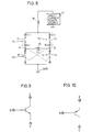
- the NPN transistor shown in Fig. 9 is used for the switching devices 11-14. Nodes C11 and E11 of Fig.
- NPN transistor 8 represent a collector and an emitter of the switching device 11 and nodes C13 and E13 represent a collector and an emitter of the switching device 13.
- the NPN transistor can be replaced by the PNP transistor shown in Fig. 10 or various devices such as FET (not shown).
- Fig. 11 is a diagram illustrating the operation of the magnetic head driving circuit shown in Fig. 8.
- (a) and (b) show waveform diagrams of the signals S1 ⁇ and S1.
- (c), (d), (e) and (f) are waveform diagrams of the voltages of the collector C13, the emitter E13, the collector C11 and the emitter E11, respectively.
- (g) shows a load impedance of the auxiliary coil 18.
- the broken lines of (d) and (e) show base voltages of the switching devices 13 and 11.
- recording data is modulated to generate signals S1 and S1 ⁇ .
- the switching devices 12 and 13 turn on in response to the signal S1 ⁇ (high level), while the switching devices 11 and 14 turn off in response to the signal S1 (low level).
- the switching devices 12 and 13 turn off, while the switching devices 11 and 14 turn on.
- the charging current of the auxiliary coil 18 flows from the direct current power source 17 to the ground terminal GND through the auxiliary coil 18, the switching device 13, the magnetic head coil 15 and the switching device 12.
- the drive current I X is supplied to the magnetic head coil 15 from the node Q toward the node P .
- the charging current of the auxiliary coil 18 flows from the direct current power source 17 to the ground terminal GND through the auxiliary coil 18, the switching device 11, the magnetic head coil 15 and the switching device 14.
- the drive current I X is supplied to the magnetic head coil 15 from the node P toward the node Q.
- the load of the auxiliary coil 18 is fixed (equal to the impedance Lx of the magnetic head coil 15) as shown in Fig. 11 (g), in response to on/off of the switching devices 12 and 13 and the switching devices 14 and 11.
- the problem of load fluctuation in the magnetic head driving circuit of Fig. 5 is therefore resolved.
- the voltage waveforms of the collectors C 13 and C 11 and those of the emitters E 13 and E 11 have a large spike-shape because of the current flowing through the auxiliary coil 18 and the magnetic head coil 15 immediately after on or off of the switching devices 12 and 13 and the switching devices 14 and 11.
- the switching device 13 Since the voltage of the emitter E 13 and the voltage of the emitter E 11 become higher than the base voltages (indicated by X in Fig. 11) because of the spike-shaped waveform, the switching device 13 remains off (not shift to an on state) immediately after the base voltage is inverted from a low level to a high level, and conversely, the switching device 11 remains on (not shift to an off state) immediately after the base voltage is inverted from a high level to a low level (Y in Fig. 11).
- the drive current I X of the magnetic head is therefore slow to rise and fall. This is because of the circuit structure wherein the switching devices 13 and 11 are placed between the auxiliary coil 18 and the magnetic head 15.
- C 13 and C 11 are voltage waveforms of the emitters of the switching devices 13 and 11, respectively
- E 13 and E 11 are voltage waveforms of the collectors of the switching devices 13 and 11, respectively
- B 13 ′ and B 11 ′ are voltage waveforms of the bases of the switching devices 13 and 11, respectively.
- the voltage waveforms of the collectors E 13 and E 11 and those of the emitters C 13 and C 11 have a large spike-shape because of the current flowing through the auxiliary coil 18 and the magnetic head coil 15 immediately after on or off of the switching devices 12 and 13 and the switching devices 14 and 11.
- the switching device 11 Since the voltage of the emitter C 13 (see Fig. 12 (c)) and the voltage of the emitter C 11 (see Fig. 12 (e)) become higher than the base voltages because of the spike-shaped waveform, the switching device 11 remains on (not shift to an off state) immediately after the base voltage B 13 ′ attains a high level (see Z in Fig. 12).
- the drive current I X of the magnetic head is slow to rise and fall. This is also because of the circuit structure wherein the switching devices 13 and 11 are located between the auxiliary coil 18 and the magnetic head coil 15.
- the description is made of NPN or PNP transistor by way of example of the switching devices 12 and 13 and the switching devices 14 and 11, it is obvious that the same problem occurs even if a switching element of FET or the like is used.
- a magnetic head circuit having improved rise and fall characteristics of a drive current to be applied to a magnetic head coil is disclosed in Japanese Patent Laying-Open No. 63-24402.
- Fig. 13 is a schematic circuit diagram of the magnetic head driving circuit disclosed in said Patent Laying-Open No. 63-24402.
- the magnetic head driving circuit shown in Fig. 13 differs from that of Fig. 8 in that a timing generator 19 is provided for generating signals S2, S3, S4 and S5 for-controlling on/off timing of the switching devices 11-14 in response to the recording signal S1.
- the signal S2 is applied to the switching device 12, the signal S3 to the switching device 11, the signal S4 to the switching device 14 and the signal S5 to the switching device 13.
- Fig. 14 is an output waveform diagram of each circuit of the magnetic head driving circuit shown in Fig. 13.
- (a) shows a waveform diagram of the recording signal S1
- (b) shows that of the signal S2
- (c) shows that of the signal S3
- (d) shows that of the signal S4
- (e) shows that of the signal S5
- (f) shows a waveform of the drive current I X .
- the switching device 11 and the switching device 14 change from on to off in response to the change of the signal S3 from a high level to a low level and the change of the signal S4 from a high level to a low level, respectively.
- the switching device 13 is turned on in response to the signal S5 which has risen earlier by a predetermined time ⁇ T 1 than the falls of said signals S3 and S4.
- the signal S3 is brought to high prior to falls of the signals S2 and S5.
- a time difference between the falls of the signals S2 and S5 and the rise of the signal S3 is represented as ⁇ T 2 .
- the switching device 11 therefore turns on before the switching devices 13 and 12 turn off.
- the present invention provides a magnetic head driving circuit for driving a magnetic head coil, comprising:
- the first current flows to the magnetic head coil through one of the first and the second auxiliary coils.
- the second current flows only to the first and the second auxiliary coils. Since the currents through the respective auxiliary coils are equal to each other, the load impedances of the respective auxiliary coils are substantially the same. Therefore, since a load impedance of each auxiliary coil can be fixed all the time, charging currents of the respective auxiliary coils can be made equal to each other at all times. Thus, it is possible to set a value of a drive current for the magnetic head coil to be equal in one direction to that of a drive current in the opposite direction, so that recording mark with reduced jitter can be recorded.
- the drive current can be normally inverted even immediately after the inversion of a recording signal. This allows the drive current to suddenly rise and fall. Furthermore, since the load of the auxiliary coil does not constantly attain zero, power consumption can be reduced.
- Claims 2 to 7 are directed to embodiments of the present invention.
- the current generating means is realized by a microcomputer.
- the microcomputer enables the magnetic head driving circuit to be made compact, which is a great advantage to the magnetic head driving circuit whose size should be small.
- Fig. 1 is a circuit diagram showing one embodiment of a magnetic head driving circuit according to the present invention.
- Fig. 2 is a timing chart of a case where data of 2-7RLL code is applied to the magnetic head driving circuit shown in Fig. 1.
- Fig. 3 is a block diagram showing another embodiment of the magnetic head driving circuit according to the present invention.
- Fig. 4 is a block diagram illustrating the principle of a magneto-optical disc apparatus.
- Fig. 5 is a circuit diagram of a conventional magnetic head driving circuit.
- Fig. 6 is a timing chart showing operation of the magnetic head driving circuit shown in Fig. 5.
- Fig. 7 is a diagram showing a bit arrangement according to the 2-7 RLL code.
- Fig. 8 is a circuit diagram of another conventional magnetic head driving circuit.
- Fig. 9 is a circuit diagram showing one example of a switching device shown in Fig. 8.
- Fig. 10 is a circuit diagram showing another example of the switching device of Fig. 8.
- Fig. 11 is a timing chart showing operation of the magnetic head driving circuit shown in Fig. 8.
- Fig. 12 is a timing chart showing operation of the magnetic head driving circuit in a case where a PNP transistor is used as the switching device in Fig. 8.
- Fig. 13 is a circuit diagram of a conventional magnetic head driving circuit.
- Fig. 14 is an output waveform diagram of each circuit of the magnetic head driving circuit shown in Fig. 13.
- Fig. 1 is a circuit diagram showing one embodiment of a magnetic head driving circuit according to the present invention.
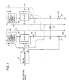
- the magnetic head driving circuit includes direct current power sources 24 and 25, dummy loads 28 and 29, switching devices 30 and 31, auxiliary coils 22 and 23, a magnetic head coil 2 l having an equivalent impedance L3, switching devices 26 and 27, and a data modulator 32.
- the data modulator 32 modulates data of a predetermined code, 2-7RLL code, for example, based on the NRZI modulation system to generate recording signals S1 and S1 complementary to each other.
- the direct current power source 24 has a negative terminal (not shown) connected to a ground terminal GND and a positive terminal (not shown) connected to one end of the dummy load 28.
- the dummy load 28 has an impedance Z1 approximately equal to the impedance L3 of the magnetic head coil 21.
- the switching device 30 is connected in parallel with the dummy load 28.
- the other end of the dummy load 28 is connected to one end of the auxiliary coil 22 (equivalent impedance of which is L1), and the other end of the auxiliary coil 22 is connected to one end (node Q 0 ) of the switching device 26.
- the other end of the switching device 26 is connected to the ground terminal GND.
- the direct current power source 25 has a negative terminal (not shown) connected to the ground terminal GND and a positive terminal (not shown) connected to one end of the dummy load 29.
- the dummy load 29 has an impedance Z2 approximately equal to the impedance L3 of the magnetic head coil 21.
- the switching device 31 is connected in parallel with the dummy load 29.
- the other end of the dummy load 29 is connected to one end of the auxiliary coil 23 (equivalent impedance of which is L2), and the other end of the auxiliary coil 23 is connected to one end (node P 0 ) of the switching device 27.
- the other end of the switching device 27 is connected to the ground terminal GND.
- the magnetic head coil 21 whose equivalent impedance is L3 is connected between the node Q 0 between the auxiliary coil 22 and the switching device 26 and the node P 0 between the auxiliary coil 23 and the switching device 27.
- the auxiliary coils 22 and 23 have impedances larger than the impedance of the magnetic head coil 21, and transmit a drive current to the magnetic head coil 21 and increase an inversion rate of the drive current.
- Both of the dummy loads 28 and 29 have the same impedances as that of the magnetic head coil 21.
- the switching devices 27 and 30 turn on/off in response to the recording signal S1, while the switching devices 26 and 31 turn on/off in response to the recording signal S1 ⁇ complementary to the recording signal S1.
- the switching devices 26, 27, 30 and 31 supply the drive current to the magnetic head coil 21 from one of the direct current power sources 24 and 25 in response to the recording signal.
- the switching devices 27 and 30 are off.
- the switching devices 27 and 30 are on, the switching devices 26 and 31 are off.
- the input recording data is modulated by the data modulator 32 and the recording signals S1 and S1 ⁇ are generated.
- the recording signal S1 is applied to the switching devices 27 and 30, while the recording signal S1 ⁇ is applied to the switching devices 26 and 31.
- the switching devices 26 and 31 and the switching devices 27 and 30 are controlled to be on or off as indicated by the solid line of Fig. 1.
- a current I 11 flows from the node P 0 toward the node Q 0
- a current I 12 flows to ground from the direct current power source 24 through the load 28, the auxiliary coil 22 and the switching device 26.
- On/off of the switching devices 26, 27, 30 and 31 is controlled in response to the recording signals S1 and S1 ⁇ to switch (invert) the direction of the drive current to be applied to the magnetic head coil 21 in this way.
- the total amount of the load for each of the auxiliary coils 22 and 23 can be made constant by on/off controlling of the switches 26, 27, 30 and 31 in this way. Description will be given later of a fixed total of the load.
- Fig. 2 is a timing chart of a case where data of the 2-7RLL code is applied to the magnetic head driving circuit shown in Fig. 1.
- (a) shows a bit arrangement of the 2-7RLL code
- (b) and (d) show the states of the recording signal S1 and the switching devices 26 and 31
- (c) and (e) show the states of the recording signal S1 and the switching devices 27 and 30,
- (f) shows a charging current IL 2 flowing through the auxiliary coil 23
- (g) shows a charging current IL 1 flowing through the auxiliary coil 22
- (h) shows a drive current flowing through the magnetic head coil 21
- (i) shows a load impedance of the auxiliary coil 22
- (j) shows a load impedance of the auxiliary coil 23.
- the switching devices 26 and 31 and the switching devices 27 and 30 are turned on/off as indicated by the solid line or the dotted line in Fig. 1 based on the recording bit of Fig. 2 (a).
- the dummy load 28 is the only load for the auxiliary coil 22.
- the load of the auxiliary coil 22 therefore totals to Z1.
- the magnetic head coil 21 is the only load for the auxiliary coil 22.
- the load of the auxiliary coil 22 therefore totals to L3.
- the load of the auxiliary coil 22 alternately totals to a value of the equivalent impedance Z1 or the equivalent impedance L3 in response to on/off of each switching device (see Fig. 2(i)).
- the magnetic head coil 21 is the only load for the auxiliary coil 23.
- the load of the auxiliary coil 23 therefore totals to L3.
- the dummy load 29 is the only load for the auxiliary coil 23.
- the load of the auxiliary coil 23 totals to Z2. In other words, the load of the auxiliary coil 23 alternately totals to the equivalent impedance L3 or the equivalent impedance Z2 (see Fig. 2 (j)).
- the recording signal whose recording bit array (see Fig. 2 (a)) is modulated includes a large amount of direct current components
- the charging current I L1 of the auxiliary coil 22 (see Fig. 2 (g)) and the charging current I L2 of the auxiliary coil 23 (see Fig. 2 (f)) are equal to each other at any time.
- the drive current to be applied to the magnetic head coil 21 therefore has a current value equal in one direction and in the opposite direction as shown in Fig. 2 (h)).
- the switching device 30 arranged between the direct current power source 24 and the auxiliary coil 22 and the switching device 31 arranged between the direct current power source 25 and the auxiliary coil 23, there exists no switch between the auxiliary coil 22 or the auxiliary coil 23 and the magnetic head coil 21.
- the switching device can be therefore turned on/off normally and reliably even if the level of the recording signal is inverted immediately after the switching operation of the switching device.
- the magnetic head coil 21 can be fully charged while reducing power consumption because the load is not zero all the time.
- the dummy loads 28 and 29 may be replaced by a register and the like having the same impedance as that of the magnetic head coil 21. It is obvious that such replacement, if enabling charging currents to the auxiliary coils to be made equal to each other constantly, produces the same effect as described above.
- Fig. 3 is a block diagram showing another embodiment of the magnetic head driving circuit according to the present invention.
- the magnetic head driving circuit shown in Fig. 3 differs from that shown in Fig. 1 in that a microcomputer 40 replaces the data modulator 32, the direct current power sources 24 and 25, the dummy loads 28 and 29 and the switching devices 30 and 31.
- the microcomputer 40 includes a data modulation portion 41 for modulating data of the 2-7RLL code on the NRZI system, a first current generation portion 42 for generating a drive current for driving the magnetic head coil 21 through one of the auxiliary coils, a second current generation portion 43 for generating a current having the same current value as that of the drive current and for charging the other of the auxiliary coils, and a current switching portion 44 for switching the connection between the first and the second current generation portions 42 and 43 and the auxiliary coils 22 and 23, respectively, in response to a recording signal generated by the data modulation portion 41.
- the first current generation portion 42 is equivalent to the direct current power source 25 and the switching device 31 in on state shown in Fig. 1.
- the second current generation portion 43 is equivalent to the circuit including the connected direct current power source 25 and the dummy load 29.
- the data modulation portion 41 modulates the input data of the 2-7RLL code to generate the recording signals S1 and S1 ⁇ .
- the current switch portion 44 connects the first current generation portion 42 to the auxiliary coil 23 and the second current generation portion 43 to the auxiliary coil 22 when the recording signal S1 ⁇ is at a high level.
- the recording signals S1 and S1 ⁇ are also applied to the switching devices 26 and 27 which are turned on and off, respectively.
- the current switch portion 44 connects the first current generation portion 42 to the auxiliary coil 22 and the second current generation portion 43 to the auxiliary coil 23. Then, the switching device 26 is turned off and the switching device 27 is turned on. Thus, a path for flowing the drive current from the node Q 0 to the node P 0 , and a path for supplying a charging current to the auxiliary coil 23 are established. As a result, completely the same operation as that of the magnetic head driving circuit of Fig. 1 can be performed.
- the use of the microcomputer 40 enables a magnetic head driving circuit to be made small in scale This is a great advantage because the magnetic head has a plurality of peripheral components.
Description
- The present invention relates to magnetic head driving circuits for driving a magnetic head for recording data on a recording medium, and more particularly, to a magnetic head driving circuit capable of over-writing data on a so-called magneto-optical disc.
- In recent years, a magnetic field modulating system magneto-optical disc apparatus has been proposed. In such a magneto-optical disc apparatus, data is written through irradiation of a recording portion of a magneto-optical disc with a laser beam of a fixed amount for applying a magnetic field to the irradiated portion.
- Fig. 4 is a block diagram explaining the principle of such magneto-optical disc apparatus. The magneto-optical disc apparatus shown in Fig. 4 comprises a magneto-
optical disc 50 having avertical magnetization film 51, alens 52 for picking up a laser beam, amagnetic head 53 and a magnetichead driving circuit 54. - Operation for over-writing the magneto-
optical disc 50 will be described. Thelens 52 narrows down a laser beam and directs the same to thevertical magnetization film 51 of the magneto-optical disc 50. The irradiation of the laser beam causes the temperature of thevertical magnetization film 51 to exceed a Curie point. The magnetichead driving circuit 54 generates a drive current I in response to input data and supplies the current I to themagnetic head 53. Themagnetic head 53 generates a magnetic field H in response to the supplied current I. Thus, the generated magnetic field is applied to the portion whose temperature exceeds the Curie point. As a result, a magnetic pattern corresponding to the input data is recorded on the magneto-optical disc 50. - In order to record data on a magneto-optical disc, however, the current technique requires a magnetic field to be generated which is stronger than that of an ordinary magnetic disc. It is therefore necessary to bring a large current to a high level or down to a low level at a high speed.
- A magnetic head circuit for resolving such problem is disclosed in Japanese Patent Laying-Open No. 63-94406.
- Fig. 5 is a circuit diagram showing the magnetic head driving circuit described in Japanese Patent Laying-Open No. 63-94406. With reference to Fig. 5, the magnetic head driving circuit comprises a
magnetic head coil 1 having an impedance Lx,auxiliary coils current power sources data modulator 8 for modulating input data (recording data) on a predetermined system to generate complementary recording signals S1,
auxiliary coil 2 is connected between a node P which is one end of themagnetic head coil 1, and the directcurrent power source 3. Theauxiliary coil 5 is connected between a node Q which is the other end of themagnetic head coil 1, and the directcurrent power source 5. Each of theauxiliary coils magnetic head coil 1. - The switching device 6 is connected between the node P and a ground terminal GND and is turned on/off in response to the recording signal S1. The switching device 7 is connected between the node Q and the ground terminal GND and is turned on/off in response to the recording signal

- Fig. 6 is a diagram showing operation of the magnetic head driving circuit shown in Fig. 5. With reference to Fig. 6, (a) is a waveform diagram of the recording signal S1, (b) a waveform diagram of the recording signal

auxiliary coil 2, (d) a waveform diagram of the charging current I2 flowing through theauxiliary coil 4, (e) a waveform diagram of the drive current Ix flowing through themagnetic head coil 1, (f) shows a load impedance of theauxiliary coil 4 and (g) shows a load impedance of theauxiliary coil 2. - With reference to Figs. 5 and 6, operation of the magnetic head driving circuit shown in Fig. 5 will be described.
- First, the
data modulator 8 modulates recording data to generate two recording signals S1 and


auxiliary coil 2 flows from the directcurrent power source 3 to the ground terminal GND through theauxiliary coil 2 and the switching device 6. At this time, the charging current I2 for charging theauxiliary coil 4 flows from the directcurrent power source 5 to the ground terminal GND through theauxiliary coil 4, themagnetic head coil 1 and the switching device 6. Thus, themagnetic head coil 1 is supplied with the drive current IX from the node Q toward the node P. - On the other hand, when the signals S1 and

auxiliary coil 4 flows from the directcurrent power source 5 to the ground terminal GND through theauxiliary coil 4 and the switching device 7. At this time, the charging current I1 for charging theauxiliary coil 2 flows from the directcurrent power source 3 to the ground terminal GND through theauxiliary coil 2, themagnetic head coil 1 and the switching device 7. The drive current IX therefore flows to themagnetic head coil 1 from the node P toward the node Q. - In response to on/off of the switching devices 6 and 7, the load of the auxiliary coil 2 (see Fig. 6 (g)) and the load of the auxiliary coil 4 (see Fig. 6 (f)) attain the impedance Lx of the magnetic head coil or 0.
- The relationship between said charging currents I1 and I2 is described in above-mentioned Japanese Patent Laying-Open No. 63-94406, wherein the inductance of the
auxiliary coils magnetic head coil 1 by Ln to establish the following equation.
- Since the relationship of the impedances is expressed as Ld >> Lx, the relationship of La >> Ln is also established, resulting in I2 ≒ I1. As is seen from the above equation, the relationship between I1 and I2 includes no factor of time. As a result, it is possible to increase an inversion rate of a drive current by setting the impedances of the
auxiliary coils magnetic head coil 1. In addition, with Ld >> Lx, Lx is substantially 0, so that load fluctuation of theauxiliary coils - However, to increase the frequencies of the recording signals S1 and

- This is followed by imbalance between the charging currents I1 and I2 of the respective
auxiliary coils magnetic head coil 1 has different values at a positive level and a negative level, so that jitter of the recording mark is increased to deteriorate the reliability of reproduced data. - The above-described problem becomes particularly conspicuous in the following case. That is, it is a case where a generally known and employed NRZI recording system (Non-return to Zero Inverse) of 2-7 RLL code (2-7 Run Length Limited) is used as modulation system for recording/reproduction in a magneto-optical disc apparatus. While such system has an advantage of increasing a recording density, it also has a disadvantage that a recording signal which recording bits are modulated includes a large amount of direct current components. It is therefore impossible to avoid the above-described problem when a recording signal of the above-described system is input to a conventional magnetic head driving circuit.
- Fig. 7 shows a bit arrangement of recording data based on the above-described 2-7 RLL code. The 2-7 RLL code includes two to seven "0" between "1" and "1". Modulation of the code by a data modulator of the NRZI system generates recording signals S1 and

- Fig. 8 is a circuit diagram of another magnetic head driving circuit disclosed in above-mentioned Japanese Patent Laying-Open No. 63-94406. With reference to Fig. 8, the magnetic head driving circuit comprises a
magnetic head coil 15,switching devices current power source 17 and anauxiliary coil 18. The relationship of the impedances between theauxiliary coil 18 and themagnetic head coil 15 is the same as that of the case shown in Fig. 5. Theswitching devices switching devices 
switching device 11 and nodes C13 and E13 represent a collector and an emitter of theswitching device 13. The NPN transistor can be replaced by the PNP transistor shown in Fig. 10 or various devices such as FET (not shown). - Fig. 11 is a diagram illustrating the operation of the magnetic head driving circuit shown in Fig. 8. With reference to Fig. 11, (a) and (b) show waveform diagrams of the signals

auxiliary coil 18. The broken lines of (d) and (e) show base voltages of theswitching devices - With reference to Figs. 8 and 11, operation of the magnetic head driving circuit shown in Fig. 8 will be described. First, recording data is modulated to generate signals S1 and

switching devices 
switching devices 
switching devices switching devices - That is, when the
switching devices switching devices auxiliary coil 18 flows from the directcurrent power source 17 to the ground terminal GND through theauxiliary coil 18, the switchingdevice 13, themagnetic head coil 15 and theswitching device 12. As a result, the drive current IX is supplied to themagnetic head coil 15 from the node Q toward the node P . - Conversely, when the
switching devices switching devices auxiliary coil 18 flows from the directcurrent power source 17 to the ground terminal GND through theauxiliary coil 18, the switchingdevice 11, themagnetic head coil 15 and theswitching device 14. As a result, the drive current IX is supplied to themagnetic head coil 15 from the node P toward the node Q. - In this related art, the load of the
auxiliary coil 18 is fixed (equal to the impedance Lx of the magnetic head coil 15) as shown in Fig. 11 (g), in response to on/off of theswitching devices switching devices - In the magnetic head driving circuit in Fig. 8, however, the voltage waveforms of the collectors C13 and C11 and those of the emitters E13 and E11 have a large spike-shape because of the current flowing through the
auxiliary coil 18 and themagnetic head coil 15 immediately after on or off of theswitching devices switching devices - Since the voltage of the emitter E13 and the voltage of the emitter E11 become higher than the base voltages (indicated by X in Fig. 11) because of the spike-shaped waveform, the switching
device 13 remains off (not shift to an on state) immediately after the base voltage is inverted from a low level to a high level, and conversely, the switchingdevice 11 remains on (not shift to an off state) immediately after the base voltage is inverted from a high level to a low level (Y in Fig. 11). - The drive current IX of the magnetic head is therefore slow to rise and fall. This is because of the circuit structure wherein the
switching devices auxiliary coil 18 and themagnetic head 15. - The use of the PNP transistor shown in Fig. 10 as the
switching devices switching devices switching devices switching devices switching devices - Description will now be made of generation of spike noise and delay in switching response in a case where a PNP transistor is used as a switching device.
- Similarly to the case of the NPN transistor, the voltage waveforms of the collectors E13 and E11 and those of the emitters C13 and C11 have a large spike-shape because of the current flowing through the
auxiliary coil 18 and themagnetic head coil 15 immediately after on or off of theswitching devices switching devices - Since the voltage of the emitter C13 (see Fig. 12 (c)) and the voltage of the emitter C11 (see Fig. 12 (e)) become higher than the base voltages because of the spike-shaped waveform, the switching
device 11 remains on (not shift to an off state) immediately after the base voltage B13′ attains a high level (see Z in Fig. 12). - Therefore, the drive current IX of the magnetic head is slow to rise and fall. This is also because of the circuit structure wherein the
switching devices auxiliary coil 18 and themagnetic head coil 15. Although the description is made of NPN or PNP transistor by way of example of theswitching devices switching devices - A magnetic head circuit having improved rise and fall characteristics of a drive current to be applied to a magnetic head coil is disclosed in Japanese Patent Laying-Open No. 63-24402.
- Fig. 13 is a schematic circuit diagram of the magnetic head driving circuit disclosed in said Patent Laying-Open No. 63-24402. The magnetic head driving circuit shown in Fig. 13 differs from that of Fig. 8 in that a
timing generator 19 is provided for generating signals S2, S3, S4 and S5 for-controlling on/off timing of the switching devices 11-14 in response to the recording signal S1. The signal S2 is applied to theswitching device 12, the signal S3 to theswitching device 11, the signal S4 to theswitching device 14 and the signal S5 to theswitching device 13. - Fig. 14 is an output waveform diagram of each circuit of the magnetic head driving circuit shown in Fig. 13. With reference to Fig. 14, (a) shows a waveform diagram of the recording signal S1, (b) shows that of the signal S2, (c) shows that of the signal S3, (d) shows that of the signal S4, (e) shows that of the signal S5 and (f) shows a waveform of the drive current IX.
- Operation of the magnetic head driving circuit shown in Fig. 13 will be described.
- When the direction of the drive current Ix is changed to flow from the node Q toward the node P, the signal S5 rises prior to falls of the signals S3 and S4. A time difference between the falls of the
signals - The switching
device 11 and theswitching device 14 change from on to off in response to the change of the signal S3 from a high level to a low level and the change of the signal S4 from a high level to a low level, respectively. The switchingdevice 13 is turned on in response to the signal S5 which has risen earlier by a predetermined time ΔT1 than the falls of said signals S3 and S4. - Conversely, when the drive current Ix is changed to flow from the node P toward the node Q, the signal S3 is brought to high prior to falls of the signals S2 and S5. A time difference between the falls of the signals S2 and S5 and the rise of the signal S3 is represented as ΔT2. The switching
device 11 therefore turns on before theswitching devices - As a result, a sufficient charging current is supplied to the auxiliary coil. When the switching device is switched, a charge generated by counter electromotive force of the coil causes the drive current to be applied to the
magnetic head coil 15 to suddenly rise and fall. - However, increasing the frequency of the recording signal S1 (increasing a data transmission rate) requires the above-described Δt1 and Δt2 to be considerably small. As a result, the auxiliary coil cannot be fully charged, so that a time required for the drive current for the magnetic head coil to rise and fall cannot be reduced.
- The foregoing problems of the related art are summarized in the following (1) to (3).
- (1) Values of a current to be applied to the magnetic head coil lose balance between positive and negative. In other words, a gap is generated between a value of the current to be applied to the coil in one direction and that of the current to be applied to the same in the opposite direction. As a result, jitter of the recording mark is increased.
- (2) Even if the level of the recording signal (base voltage) is switched, the switch remains off immediately after that, whereby the drive current to be applied to the coil is caused to rise and fall slowly.
- (3) Increase in a rate for recording data is followed by a reduction of charging time, resulting in insufficient charging of the auxiliary coil. It is therefore impossible to cause the drive current to be applied to the coil to suddenly rise and fall.
- Thus, it is difficult for any of the related art to record data of such as 2-7RLL code at a high speed.
- The present invention, as defined by
claim 1, provides a magnetic head driving circuit for driving a magnetic head coil, comprising: - a first auxiliary coil having an impedance larger than an impedance of said magnetic head coil and connected to one end of said magnetic head coil;
- a second auxiliary coil having an impedance larger than the impedance of said magnetic head coil and connected to the other end of said magnetic head coil;
- current generating means for generating a first current for charging one of said auxiliary coils and driving said magnetic head coil, and a second current for charging the other of said auxiliary coils; and
- path forming means responsive to input data for forming a first path for supplying said first current to said magnetic head coil through one of the auxiliary coils, and a second path for supplying said second current to the other of the auxiliary coils;
- said current generating means generates said first and second currents in response to said input data; and
- said first and second currents provide for equal currents to flow simultaneously in the two auxiliary coils independently of which auxiliary coil supplies current to the head coil.
- In operation, the first current flows to the magnetic head coil through one of the first and the second auxiliary coils. The second current flows only to the first and the second auxiliary coils. Since the currents through the respective auxiliary coils are equal to each other, the load impedances of the respective auxiliary coils are substantially the same. Therefore, since a load impedance of each auxiliary coil can be fixed all the time, charging currents of the respective auxiliary coils can be made equal to each other at all times. Thus, it is possible to set a value of a drive current for the magnetic head coil to be equal in one direction to that of a drive current in the opposite direction, so that recording mark with reduced jitter can be recorded.
- In addition, with no switch provided between the auxiliary coil and the magnetic head coil, the drive current can be normally inverted even immediately after the inversion of a recording signal. This allows the drive current to suddenly rise and fall. Furthermore, since the load of the auxiliary coil does not constantly attain zero, power consumption can be reduced.
- In addition, with one of the first and second currents being supplied to each auxiliary coil, constant charging of the auxiliary coil is possible, thereby enabling the auxiliary coil to be sufficiently charged. This also enables the drive current of the magnetic head coil to suddenly rise and fall.
-
Claims 2 to 7 are directed to embodiments of the present invention. - In one embodiment, the current generating means is realized by a microcomputer. The microcomputer enables the magnetic head driving circuit to be made compact, which is a great advantage to the magnetic head driving circuit whose size should be small.
- According to the present invention, it becomes possible:
- (1) to record data at a high speed by providing the same amount of currents to a magnetic head coil in one direction and in the opposition direction in a magnetic head driving circuit;
- (2) to record data at a high speed in a magnetic head driving circuit while reducing spike noise caused by a direction change of a drive current; and
- (3) to record data at a high speed in a magnetic head driving circuit without delaying a recording signal.
- Fig. 1 is a circuit diagram showing one embodiment of a magnetic head driving circuit according to the present invention.
- Fig. 2 is a timing chart of a case where data of 2-7RLL code is applied to the magnetic head driving circuit shown in Fig. 1.
- Fig. 3 is a block diagram showing another embodiment of the magnetic head driving circuit according to the present invention.
- Fig. 4 is a block diagram illustrating the principle of a magneto-optical disc apparatus.
- Fig. 5 is a circuit diagram of a conventional magnetic head driving circuit.
- Fig. 6 is a timing chart showing operation of the magnetic head driving circuit shown in Fig. 5.
- Fig. 7 is a diagram showing a bit arrangement according to the 2-7 RLL code.
- Fig. 8 is a circuit diagram of another conventional magnetic head driving circuit.
- Fig. 9 is a circuit diagram showing one example of a switching device shown in Fig. 8.
- Fig. 10 is a circuit diagram showing another example of the switching device of Fig. 8.
- Fig. 11 is a timing chart showing operation of the magnetic head driving circuit shown in Fig. 8.
- Fig. 12 is a timing chart showing operation of the magnetic head driving circuit in a case where a PNP transistor is used as the switching device in Fig. 8.
- Fig. 13 is a circuit diagram of a conventional magnetic head driving circuit.
- Fig. 14 is an output waveform diagram of each circuit of the magnetic head driving circuit shown in Fig. 13.
- Fig. 1 is a circuit diagram showing one embodiment of a magnetic head driving circuit according to the present invention. With reference to Fig. 1, the magnetic head driving circuit includes direct
current power sources devices 30 and 31,auxiliary coils magnetic head coil 2l having an equivalent impedance L3, switchingdevices data modulator 32. - The data modulator 32 modulates data of a predetermined code, 2-7RLL code, for example, based on the NRZI modulation system to generate recording signals S1 and S1 complementary to each other.
- The direct
current power source 24 has a negative terminal (not shown) connected to a ground terminal GND and a positive terminal (not shown) connected to one end of thedummy load 28. Thedummy load 28 has an impedance Z1 approximately equal to the impedance L3 of themagnetic head coil 21. - The switching device 30 is connected in parallel with the
dummy load 28. The other end of thedummy load 28 is connected to one end of the auxiliary coil 22 (equivalent impedance of which is L1), and the other end of theauxiliary coil 22 is connected to one end (node Q0) of theswitching device 26. The other end of theswitching device 26 is connected to the ground terminal GND. - The direct
current power source 25 has a negative terminal (not shown) connected to the ground terminal GND and a positive terminal (not shown) connected to one end of thedummy load 29. Thedummy load 29 has an impedance Z2 approximately equal to the impedance L3 of themagnetic head coil 21. - The switching
device 31 is connected in parallel with thedummy load 29. The other end of thedummy load 29 is connected to one end of the auxiliary coil 23 (equivalent impedance of which is L2), and the other end of theauxiliary coil 23 is connected to one end (node P0) of theswitching device 27. The other end of theswitching device 27 is connected to the ground terminal GND. - The
magnetic head coil 21 whose equivalent impedance is L3 is connected between the node Q0 between theauxiliary coil 22 and theswitching device 26 and the node P0 between theauxiliary coil 23 and theswitching device 27. - The auxiliary coils 22 and 23 have impedances larger than the impedance of the
magnetic head coil 21, and transmit a drive current to themagnetic head coil 21 and increase an inversion rate of the drive current. Both of the dummy loads 28 and 29 have the same impedances as that of themagnetic head coil 21. - The
switching devices 27 and 30 turn on/off in response to the recording signal S1, while theswitching devices 
- More specifically, the
switching devices magnetic head coil 21 from one of the directcurrent power sources switching devices switching devices 27 and 30 are off. On the other hand, when theswitching devices 27 and 30 are on, theswitching devices - Operation of the magnetic head driving circuit shown in Fig. 1 will be described in the following. The input recording data is modulated by the
data modulator 32 and the recording signals S1 and
switching devices 27 and 30, while the recording signal
switching devices - In a case where the drive current is applied to the
magnetic head coil 21 from the node P0 toward the node Q0 in Fig. 1, for example, theswitching devices switching devices 27 and 30 are controlled to be on or off as indicated by the solid line of Fig. 1. At this time, a current I11 (flowing from the node P0 toward the node Q0) is applied to themagnetic head coil 21 from the directcurrent power source 25 through the switchingdevice 31 and theauxiliary coil 23, while a current I12 flows to ground from the directcurrent power source 24 through theload 28, theauxiliary coil 22 and theswitching device 26. - Conversely, when the drive current is applied to the
magnetic head coil 21 from the node Q0 toward the node P0 in Fig. 1, theswitching devices switching devices 27 and 30 are controlled to be on or off as indicated by the dotted line of Fig. 1. At this time, a current I21 (flowing from the node Q0 toward the node P0) is applied to themagnetic head coil 21 from the directcurrent source 24 through the switching device 30 and theauxiliary coil 22, while a current I22 flows to ground from the directcurrent power source 25 through theload 29, theauxiliary coil 23 and theswitching device 27. - On/off of the
switching devices 
magnetic head coil 21 in this way. The total amount of the load for each of theauxiliary coils switches - Following is description of recording and reproduction of the recording bit array shown in Fig. 2(a) by using the NRZI recording system for the 2-7RLL code shown in Fig. 7 as a recording/reproduction system in a magneto-optical disc apparatus.
- Fig. 2 is a timing chart of a case where data of the 2-7RLL code is applied to the magnetic head driving circuit shown in Fig. 1. With reference to Fig. 2, (a) shows a bit arrangement of the 2-7RLL code, (b) and (d) show the states of the recording signal S1 and the
switching devices switching devices 27 and 30, (f) shows a charging current IL2 flowing through theauxiliary coil 23, (g) shows a charging current IL1 flowing through theauxiliary coil 22, (h) shows a drive current flowing through themagnetic head coil 21, (i) shows a load impedance of theauxiliary coil 22 and (j) shows a load impedance of theauxiliary coil 23. - Operation for recording data of the 2-7RLL code will be described in the following.
- The
switching devices switching devices 27 and 30 are turned on/off as indicated by the solid line or the dotted line in Fig. 1 based on the recording bit of Fig. 2 (a). - When the respective switching devices are controlled to be on/off as indicated by the solid line of Fig. 1, the
dummy load 28 is the only load for theauxiliary coil 22. The load of theauxiliary coil 22 therefore totals to Z1. When the above-described respective switching devices are controlled to be on/off as ind-icated by the dotted line of Fig. 1, themagnetic head coil 21 is the only load for theauxiliary coil 22. The load of theauxiliary coil 22 therefore totals to L3. In other words, the load of theauxiliary coil 22 alternately totals to a value of the equivalent impedance Z1 or the equivalent impedance L3 in response to on/off of each switching device (see Fig. 2(i)). - Similarly, when the
switching devices switching devices 27 and 30 are controlled to be on/off as indicated by the solid line of Fig. 1, themagnetic head coil 21 is the only load for theauxiliary coil 23. The load of theauxiliary coil 23 therefore totals to L3. When the above-described respective switching devices are controlled to be on/off as indicated by the dotted line of Fig. 1, thedummy load 29 is the only load for theauxiliary coil 23. The load of theauxiliary coil 23 totals to Z2. In other words, the load of theauxiliary coil 23 alternately totals to the equivalent impedance L3 or the equivalent impedance Z2 (see Fig. 2 (j)). - Herein, assuming that both of the dummy loads 28 and 29 have the same impedance as that of the magnetic head coil 21 (ZI = Z2 = L3), the total of each load of the
auxiliary coils switching devices switching devices 27 and 30 are controlled to be on/off as indicated by the solid line or the dotted line of Fig. 1. - In other words, although the recording signal whose recording bit array (see Fig. 2 (a)) is modulated includes a large amount of direct current components, the charging current IL1 of the auxiliary coil 22 (see Fig. 2 (g)) and the charging current IL2 of the auxiliary coil 23 (see Fig. 2 (f)) are equal to each other at any time. The drive current to be applied to the
magnetic head coil 21 therefore has a current value equal in one direction and in the opposite direction as shown in Fig. 2 (h)). - In addition, with the switching device 30 arranged between the direct
current power source 24 and theauxiliary coil 22 and theswitching device 31 arranged between the directcurrent power source 25 and theauxiliary coil 23, there exists no switch between theauxiliary coil 22 or theauxiliary coil 23 and themagnetic head coil 21. The switching device can be therefore turned on/off normally and reliably even if the level of the recording signal is inverted immediately after the switching operation of the switching device. - Furthermore, since the
auxiliary coils switching devices switching devices 27 and 30, themagnetic head coil 21 can be fully charged while reducing power consumption because the load is not zero all the time. - The dummy loads 28 and 29 may be replaced by a register and the like having the same impedance as that of the
magnetic head coil 21. It is obvious that such replacement, if enabling charging currents to the auxiliary coils to be made equal to each other constantly, produces the same effect as described above. - Fig. 3 is a block diagram showing another embodiment of the magnetic head driving circuit according to the present invention.
- The magnetic head driving circuit shown in Fig. 3 differs from that shown in Fig. 1 in that a
microcomputer 40 replaces thedata modulator 32, the directcurrent power sources switching devices 30 and 31. Themicrocomputer 40 includes adata modulation portion 41 for modulating data of the 2-7RLL code on the NRZI system, a firstcurrent generation portion 42 for generating a drive current for driving themagnetic head coil 21 through one of the auxiliary coils, a secondcurrent generation portion 43 for generating a current having the same current value as that of the drive current and for charging the other of the auxiliary coils, and acurrent switching portion 44 for switching the connection between the first and the secondcurrent generation portions auxiliary coils data modulation portion 41. - The first
current generation portion 42 is equivalent to the directcurrent power source 25 and theswitching device 31 in on state shown in Fig. 1. The secondcurrent generation portion 43 is equivalent to the circuit including the connected directcurrent power source 25 and thedummy load 29. - In operation, the
data modulation portion 41 modulates the input data of the 2-7RLL code to generate the recording signals S1 and
current switch portion 44 connects the firstcurrent generation portion 42 to theauxiliary coil 23 and the secondcurrent generation portion 43 to theauxiliary coil 22 when the recording signal

switching devices magnetic head coil 21 and a path for supplying a charging current to theauxiliary coil 22 are established. - Conversely, when the recording signal

current switch portion 44 connects the firstcurrent generation portion 42 to theauxiliary coil 22 and the secondcurrent generation portion 43 to theauxiliary coil 23. Then, the switchingdevice 26 is turned off and theswitching device 27 is turned on. Thus, a path for flowing the drive current from the node Q0 to the node P0, and a path for supplying a charging current to theauxiliary coil 23 are established. As a result, completely the same operation as that of the magnetic head driving circuit of Fig. 1 can be performed. - In addition, the use of the
microcomputer 40 enables a magnetic head driving circuit to be made small in scale This is a great advantage because the magnetic head has a plurality of peripheral components. - Although the present invention has been described and illustrated in detail, it is clearly understood that the same is by way of illustration and example only and is not to be taken by way of limitation, the spirit and scope of the present invention being limited only by the terms of the appended claims.
Claims (7)
- A magnetic head driving circuit for driving a magnetic head coil (21), comprising:a first auxiliary coil (22) having an impedance (L1) larger than an impedance (L3) of said magnetic head coil and connected to one end of said magnetic head coil;a second auxiliary coil (23) having an impedance (L2) larger than the impedance of said magnetic head coil and connected to the other end of said magnetic head coil;current generating means (24,25;42,43) for generating a first current for charging one of said auxiliary coils and driving said magnetic head coil, and a second current for charging the other of said auxiliary coils; andpath forming means (26,27) responsive to input data for forming a first path for supplying said first current to said magnetic head coil through one of the auxiliary coils, and a second path for supplying said second current to the other of the auxiliary coils;characterized in that:said current generating means (24,25,28,29,30, 31,32;41,42,43,44) generates said first and second currents in response to said input data; andsaid first and second currents provide for equal currents to flow simultaneously in the two auxiliary coils (22,23) independently of which auxiliary coil supplies current to the head coil (21).
- The magnetic head driving circuit according to claim 1, wherein said current generating means includes:data modulating means (32) for modulating said input data to generate a recording signal (S1,
 first current generating means (24, 28, 30) responsive to one state of said recording signal for generating said first current and responsive to the other state of said recording signal for generating said second current, andsecond current generating means (25, 29, 31) responsive to one state of said recording signal for generating said second current and responsive to the other state of said recording signal for generating said first current.
 - The magnetic head driving circuit according to claim 2, whereinsaid first current generating means includes:a first direct current power source (24) for generating a direct current,first switching means (30) connected between said first direct current power source and said first auxiliary coil and being turned on/off in response to said recording signal, andfirst dummy load means (28) having the same impedance (Z1) as that of said magnetic head coil and connected in parallel with said first switching means; andsaid second current generating means includes:a second direct current power source (25) for generating a direct current,second switching means (31) connected between said second direct current power source and said second auxiliary coil and being turned on/off complementarily with said first switching means (30) in response to said recording signal, andsecond dummy load means (29) having the same impedance (Z2) as that of said magnetic head coil and connected in parallel with said second switching means.
- The magnetic head driving circuit according to claim 1, wherein said current generating means includes a microcomputer (40), said microcomputer including:first current generating means (42) for generating said first current,second current generating means (43) for generating said second current,data modulating means (41) for modulating said input data to generate a recording signal (S1,
 means (44) responsive to one state of said generated recording signal for supplying said generated first current to one of the first and second auxiliary coils and said generated second current to the other of the said first and second auxiliary coils, and responsive to the other state of said recording signal for supplying said generated first current to said other of the first and second auxiliary coils and said generated second current to said one of the first and second auxiliary coils.
 - The magnetic head driving circuit according to any preceding claim, wherein said path forming means includes:third switching means (26) connected between one and of said magnetic head coil and a ground terminal and being turned on/off in response to said input data, andfourth switching means (27) connected between the other end of said magnetic head coil and the ground terminal and being turned on/off complementarily with said third switching means (26) in response to said input data.
- The magnetic head driving circuit according to any preceding claim, wherein said input data include data having a long succession of bits of the same logic.
- The magnetic head driving circuit according to claim 6, wherein said input data include data having a succession of two to seven bits of the same logic.
Applications Claiming Priority (2)
| Application Number | Priority Date | Filing Date | Title |
|---|---|---|---|
| JP3150478A JP2795757B2 (en) | 1991-06-21 | 1991-06-21 | Magnetic head drive circuit |
| JP150478/91 | 1991-06-21 |
Publications (3)
| Publication Number | Publication Date |
|---|---|
| EP0519729A2 EP0519729A2 (en) | 1992-12-23 |
| EP0519729A3 EP0519729A3 (en) | 1993-06-09 |
| EP0519729B1 true EP0519729B1 (en) | 1996-08-21 |
Family
ID=15497772
Family Applications (1)
| Application Number | Title | Priority Date | Filing Date |
|---|---|---|---|
| EP92305631A Expired - Lifetime EP0519729B1 (en) | 1991-06-21 | 1992-06-19 | Magnetic head driving circuit |
Country Status (5)
| Country | Link |
|---|---|
| US (1) | US5359466A (en) |
| EP (1) | EP0519729B1 (en) |
| JP (1) | JP2795757B2 (en) |
| CA (1) | CA2071592C (en) |
| DE (1) | DE69212916T2 (en) |
Families Citing this family (15)
| Publication number | Priority date | Publication date | Assignee | Title |
|---|---|---|---|---|
| US5587851A (en) * | 1991-12-24 | 1996-12-24 | Sharp Kabushiki Kaisha | Magnetic head driving device with prerecording energization |
| JP2859766B2 (en) * | 1991-12-24 | 1999-02-24 | シャープ株式会社 | Magnetic head drive circuit |
| JP3211999B2 (en) * | 1992-06-26 | 2001-09-25 | キヤノン株式会社 | Magneto-optical recording device |
| JP3107265B2 (en) * | 1993-08-06 | 2000-11-06 | キヤノン株式会社 | Magnetic head drive device and magnetic recording device |
| JP2977710B2 (en) * | 1993-10-26 | 1999-11-15 | ティーディーケイ株式会社 | Modulated magnetic field generator for magneto-optical recording and magneto-optical recording device |
| JPH07182717A (en) * | 1993-12-24 | 1995-07-21 | Sharp Corp | Optical magnetic recording/reproducing device |
| JP3659988B2 (en) * | 1994-07-14 | 2005-06-15 | シャープ株式会社 | Magneto-optical recording device |
| JP3109387B2 (en) * | 1994-09-26 | 2000-11-13 | キヤノン株式会社 | Magnetic head drive circuit |
| US6031807A (en) * | 1997-05-07 | 2000-02-29 | Stmicroelectronics, Inc. | Programming the inductance of read/write heads |
| US6005733A (en) * | 1997-06-12 | 1999-12-21 | Vtc, Inc. | Preamplifier bias circuit for use in an AC coupled magnetoresistive read head amplifier |
| JP2001176142A (en) * | 1999-12-16 | 2001-06-29 | Canon Inc | Magnetic head drive circuit and magneto-optical recorder |
| JP2005051021A (en) * | 2003-07-28 | 2005-02-24 | Sharp Corp | Magnetic coupling element and electronic instrument using it |
| US8310777B2 (en) * | 2009-09-09 | 2012-11-13 | International Business Machines Corporation | Systems and methods for reducing crosstalk between adjacent writers |
| TWI513168B (en) * | 2012-12-20 | 2015-12-11 | Compal Electronics Inc | Power conversion apparatus |
| US9799351B1 (en) | 2015-11-30 | 2017-10-24 | Western Digital (Fremont), Llc | Short yoke length writer having assist coils |
Family Cites Families (5)
| Publication number | Priority date | Publication date | Assignee | Title |
|---|---|---|---|---|
| JPH0743805B2 (en) * | 1986-10-07 | 1995-05-15 | ソニー株式会社 | Magnetic head drive circuit |
| JPS63244402A (en) * | 1987-03-31 | 1988-10-11 | Sony Corp | Magnetic field generating circuit for recording |
| DE3836125A1 (en) * | 1988-10-22 | 1990-05-03 | Thomson Brandt Gmbh | CIRCUIT ARRANGEMENT FOR REVERSING A MAGNETIC FIELD |
| DE3838858A1 (en) * | 1988-11-17 | 1990-05-23 | Thomson Brandt Gmbh | CIRCUIT ARRANGEMENT FOR REVERSING A MAGNETIC FIELD |
| JPH03157839A (en) * | 1989-11-15 | 1991-07-05 | Matsushita Electric Ind Co Ltd | High frequency modulated magnetic field generating device for magneto-optical disk |
-
1991
- 1991-06-21 JP JP3150478A patent/JP2795757B2/en not_active Expired - Fee Related
-
1992
- 1992-06-18 CA CA002071592A patent/CA2071592C/en not_active Expired - Fee Related
- 1992-06-19 EP EP92305631A patent/EP0519729B1/en not_active Expired - Lifetime
- 1992-06-19 US US07/901,025 patent/US5359466A/en not_active Expired - Lifetime
- 1992-06-19 DE DE69212916T patent/DE69212916T2/en not_active Expired - Fee Related
Also Published As
| Publication number | Publication date |
|---|---|
| CA2071592C (en) | 1997-02-11 |
| EP0519729A3 (en) | 1993-06-09 |
| US5359466A (en) | 1994-10-25 |
| DE69212916T2 (en) | 1997-02-20 |
| JPH04372701A (en) | 1992-12-25 |
| JP2795757B2 (en) | 1998-09-10 |
| EP0519729A2 (en) | 1992-12-23 |
| DE69212916D1 (en) | 1996-09-26 |
| CA2071592A1 (en) | 1992-12-22 |
Similar Documents
| Publication | Publication Date | Title |
|---|---|---|
| EP0519729B1 (en) | Magnetic head driving circuit | |
| EP0304298B1 (en) | Magnetic head drive circuit | |
| EP0183849B1 (en) | Control circuit that operates on pulse-width modulated signals | |
| EP0469929B1 (en) | Controlling currents in laser diodes | |
| KR970001977B1 (en) | Optical-magneto recording apparatus | |
| CA2178882C (en) | Magnetic recording device and method | |
| JPH02166636A (en) | Laser driving circuit | |
| US5329408A (en) | Magnetic field modulation magnet-optical recording apparatus in which an FM modulator and a magnetic head driving circuit are used in common | |
| JPH03157839A (en) | High frequency modulated magnetic field generating device for magneto-optical disk | |
| JPH03198204A (en) | Magnetic head driving circuit | |
| JPH0626275B2 (en) | Semiconductor laser drive circuit | |
| JPH08147697A (en) | Semiconductor laser driving circuit | |
| JPH0253229A (en) | Impedance load driving circuit | |
| US5448422A (en) | Magnetic head drive circuit including capacitors for storing charge to drive a magnetic head coil | |
| KR950013705B1 (en) | Fm modulation & magnetic head driving circuit of magnetic moduktion aptical magnetic recording apparatus | |
| US6477119B2 (en) | Magnetic head drive circuit including paired auxiliary coils, paired switching elements, and switch element control circuit, and magneto-optical recording device using the same | |
| JP2550842B2 (en) | High frequency modulation magnetic field generation circuit | |
| JP2845411B2 (en) | Recording magnetic field generating method and apparatus | |
| US6856582B2 (en) | Method for driving magnetic head and driving circuit of magneto-optical disk drive | |
| JP3144601B2 (en) | Magnetic head drive | |
| JPH079212Y2 (en) | Laser drive circuit | |
| JPS62150531A (en) | Focus controller | |
| JPH0845008A (en) | Recording and reproducing device | |
| JPH03272038A (en) | Magnetic head device | |
| JPH04219601A (en) | Magnetic head driving circuit |
Legal Events
| Date | Code | Title | Description |
|---|---|---|---|
| PUAI | Public reference made under article 153(3) epc to a published international application that has entered the european phase |
Free format text: ORIGINAL CODE: 0009012 |
|
| AK | Designated contracting states |
Kind code of ref document: A2 Designated state(s): DE FR GB IT NL |
|
| PUAL | Search report despatched |
Free format text: ORIGINAL CODE: 0009013 |
|
| AK | Designated contracting states |
Kind code of ref document: A3 Designated state(s): DE FR GB IT NL |
|
| 17P | Request for examination filed |
Effective date: 19930721 |
|
| 17Q | First examination report despatched |
Effective date: 19950825 |
|
| GRAH | Despatch of communication of intention to grant a patent |
Free format text: ORIGINAL CODE: EPIDOS IGRA |
|
| GRAH | Despatch of communication of intention to grant a patent |
Free format text: ORIGINAL CODE: EPIDOS IGRA |
|
| GRAA | (expected) grant |
Free format text: ORIGINAL CODE: 0009210 |
|
| AK | Designated contracting states |
Kind code of ref document: B1 Designated state(s): DE FR GB IT NL |
|
| PG25 | Lapsed in a contracting state [announced via postgrant information from national office to epo] |
Ref country code: IT Free format text: LAPSE BECAUSE OF FAILURE TO SUBMIT A TRANSLATION OF THE DESCRIPTION OR TO PAY THE FEE WITHIN THE PRE;WARNING: LAPSES OF ITALIAN PATENTS WITH EFFECTIVE DATE BEFORE 2007 MAY HAVE OCCURRED AT ANY TIME BEFORE 2007. THE CORRECT EFFECTIVE DATE MAY BE DIFFERENT FROM THE ONE RECORDED.SCRIBED TIME-LIMIT Effective date: 19960821 |
|
| REF | Corresponds to: |
Ref document number: 69212916 Country of ref document: DE Date of ref document: 19960926 |
|
| ET | Fr: translation filed | ||
| PLBE | No opposition filed within time limit |
Free format text: ORIGINAL CODE: 0009261 |
|
| STAA | Information on the status of an ep patent application or granted ep patent |
Free format text: STATUS: NO OPPOSITION FILED WITHIN TIME LIMIT |
|
| 26N | No opposition filed | ||
| REG | Reference to a national code |
Ref country code: GB Ref legal event code: IF02 |
|
| PGFP | Annual fee paid to national office [announced via postgrant information from national office to epo] |
Ref country code: NL Payment date: 20020628 Year of fee payment: 11 |
|
| PG25 | Lapsed in a contracting state [announced via postgrant information from national office to epo] |
Ref country code: NL Free format text: LAPSE BECAUSE OF NON-PAYMENT OF DUE FEES Effective date: 20040101 |
|
| NLV4 | Nl: lapsed or anulled due to non-payment of the annual fee |
Effective date: 20040101 |
|
| PGFP | Annual fee paid to national office [announced via postgrant information from national office to epo] |
Ref country code: DE Payment date: 20080626 Year of fee payment: 17 |
|
| PGFP | Annual fee paid to national office [announced via postgrant information from national office to epo] |
Ref country code: FR Payment date: 20080617 Year of fee payment: 17 |
|
| PGFP | Annual fee paid to national office [announced via postgrant information from national office to epo] |
Ref country code: GB Payment date: 20080625 Year of fee payment: 17 |
|
| GBPC | Gb: european patent ceased through non-payment of renewal fee |
Effective date: 20090619 |
|
| REG | Reference to a national code |
Ref country code: FR Ref legal event code: ST Effective date: 20100226 |
|
| PG25 | Lapsed in a contracting state [announced via postgrant information from national office to epo] |
Ref country code: FR Free format text: LAPSE BECAUSE OF NON-PAYMENT OF DUE FEES Effective date: 20090630 |
|
| PG25 | Lapsed in a contracting state [announced via postgrant information from national office to epo] |
Ref country code: GB Free format text: LAPSE BECAUSE OF NON-PAYMENT OF DUE FEES Effective date: 20090619 |
|
| PG25 | Lapsed in a contracting state [announced via postgrant information from national office to epo] |
Ref country code: DE Free format text: LAPSE BECAUSE OF NON-PAYMENT OF DUE FEES Effective date: 20100101 |