EP0513663B1 - Simplified low-noise output buffer circuit - Google Patents
Simplified low-noise output buffer circuit Download PDFInfo
- Publication number
- EP0513663B1 EP0513663B1 EP92107713A EP92107713A EP0513663B1 EP 0513663 B1 EP0513663 B1 EP 0513663B1 EP 92107713 A EP92107713 A EP 92107713A EP 92107713 A EP92107713 A EP 92107713A EP 0513663 B1 EP0513663 B1 EP 0513663B1
- Authority
- EP
- European Patent Office
- Prior art keywords
- terminal
- output
- coupled
- control
- potential
- Prior art date
- Legal status (The legal status is an assumption and is not a legal conclusion. Google has not performed a legal analysis and makes no representation as to the accuracy of the status listed.)
- Expired - Lifetime
Links
Images


Classifications
-
- G—PHYSICS
- G11—INFORMATION STORAGE
- G11C—STATIC STORES
- G11C7/00—Arrangements for writing information into, or reading information out from, a digital store
-
- H—ELECTRICITY
- H03—ELECTRONIC CIRCUITRY
- H03K—PULSE TECHNIQUE
- H03K19/00—Logic circuits, i.e. having at least two inputs acting on one output; Inverting circuits
- H03K19/02—Logic circuits, i.e. having at least two inputs acting on one output; Inverting circuits using specified components
- H03K19/08—Logic circuits, i.e. having at least two inputs acting on one output; Inverting circuits using specified components using semiconductor devices
- H03K19/094—Logic circuits, i.e. having at least two inputs acting on one output; Inverting circuits using specified components using semiconductor devices using field-effect transistors
- H03K19/09425—Multistate logic
- H03K19/09429—Multistate logic one of the states being the high impedance or floating state
-
- H—ELECTRICITY
- H03—ELECTRONIC CIRCUITRY
- H03K—PULSE TECHNIQUE
- H03K19/00—Logic circuits, i.e. having at least two inputs acting on one output; Inverting circuits
- H03K19/003—Modifications for increasing the reliability for protection
- H03K19/00346—Modifications for eliminating interference or parasitic voltages or currents
- H03K19/00361—Modifications for eliminating interference or parasitic voltages or currents in field effect transistor circuits
Definitions
- This invention relates to an output buffer circuit, more particularly to an output buffer circuit with a simple circuit configuration and reduced switching noise.
- Switching noise occurring on power supply and ground lines when an output buffer is switched between different states is a serious problem in integrated circuits.
- the major cause of such noise is the abrupt charging or discharging of a capacitive output load to which the buffer is connected.
- a minor cause is direct flow of current from the power supply to ground through the buffer circuit at the instant of switching.
- Japanese Patent Application Kokai Publication No. 216518/1986 discloses a tri-state output buffer circuit with two field-effect output transistors, the gates of which are interconnected through a transmission gate that is switched on and off by a control signal.
- the transmission gate reduces switching noise by delaying the turn-on times of the output transistors, so that they are never both on simultaneously. This scheme eliminates the minor cause of the switching noise problem, but fails to address the major cause.
- Japanese Patent Application Kokai Publication No. 244124/1986 discloses an output buffer circuit having two or more pull-up output transistors coupled in parallel to the power supply, and two or more pull-down output transistors coupled in parallel to ground.
- the turn-on times of the transistors are staggered so as to reduce peak charge or discharge current, while providing sufficient current-driving ability after all pull-up or pull-down transistors have been turned on.
- the drawback of this scheme is the large number of circuit elements required, e.g. twenty-four transistors in the disclosed circuit, many having their drains connected directly to the output terminal and requiring large pattern areas to prevent such problems as latch-up. This scheme is accordingly inappropriate for gate arrays and other devices in which a large number of output buffers must fit into a restricted space.
- EP-A-0 344 604 discloses an output buffer, wherein a resistive circuit of CMOS structure is connected between the gates of the CMOS transistors.
- the resistive circuit reduces the changes in the gate potentials of output buffer transistors, which occur when logic inputs are supplied to the gates of the output control transistors. Hence, the deformation of the output waveform, which has resulted from the through currents flowing through the output buffer transistors, is minimized.
- the output buffer of EP-A-0 344 604 is similar to the output buffer disclosed in the above-mentioned Japanese Application Kokai Publication No. 216518/1986, the features of which are also described in the preamble of claim 1.
- Another object of the present invention is to simplify the structure of output buffer circuits.
- Yet another object of the invention is to improve the switching speed of output buffer circuits.
- the objects are solved by an output buffer as defined in claim 1.
- the subclaims show further developments of the output buffer of claim 1.
- the invented output buffer circuit has an output terminal, a power supply terminal, and a ground terminal.
- the output terminal is coupled to the power supply terminal through first switch having a first control terminal, the coupling being responsive to input at the first control terminal.
- the output terminal is coupled to the ground terminal through second switch having a second control terminal, the coupling being responsive to input at the second control terminal.
- the first control terminal and second terminal are mutually coupled through a third switch.
- the third switch is also coupled to the output terminal, and the mutual coupling of the first and second control terminals is responsive to the potential of the output terminal.
- Fig. 1 is a schematic diagram of a novel tri-state output buffer circuit.
- Fig. 2 is a partial redrawing of Fig. 1, illustrating a load capacitance and stray inductance.
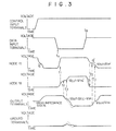
- Fig. 3 is a waveform diagram illustrating the operation of the output buffer circuit in Fig. 1.
- Fig. 4 is a schematic diagram of a prior-art output buffer circuit.
- Fig. 5 is a graph of peak ground noise voltages in novel and prior-art output buffer circuits.
- Fig. 6 is a schematic diagram of a novel totem-pole output buffer circuit.
- a novel tri-state output buffer circuit has a data input terminal 1, a control input terminal 2, an output terminal 3, a power supply terminal 4, and a ground terminal 5.
- the power supply and ground terminals 4 and 5 are coupled to internal power supply and ground lines of an integrated circuit of which the output buffer circuit in Fig. 1 is a part.
- the ground terminal 5 supplies a nominally constant ground potential.
- V CC and GND will be used to denote the power supply and ground potentials.
- the terms “high” and “low” will also be used to refer to the power-supply and ground potentials, respectively. In the following descriptions a power-supply potential of five volts and ground potential of zero volts will be assumed, but the invention is of course not limited to these specific values.
- the output buffer circuit in Fig. 1 is divided into three stages.
- a final output stage 8 directly drives the output terminal 3.
- a switching stage 10 (the semiconductor switching means referred to in the summary of the invention) turns on elements in the final stage 8.
- a control stage 12 controls the switching stage 10, and turns off elements in the final stage.
- the final stage 8 comprises a pull-up output transistor and a pull-down output transistor.
- the pull-up output transistor is a p-channel metal-oxide-semiconductor field-effect output transistor 14 with a source electrode coupled to the power supply terminal 4, a gate electrode coupled to a first node 15, and a drain electrode coupled to the output terminal 3.
- the pull-down output transistor is an n-channel metal-oxide-semiconductor field-effect output transistor 16 with a source electrode coupled to the ground terminal 5, a gate electrode coupled to a second node 18, and a drain electrode coupled to the output terminal 3.
- p-channel and n-channel metal-oxide-semiconductor field-effect transistors will be referred to below by the standard acronyms PMOS and NMOS, the word “electrode” will be omitted, and nodes will be identified only by their reference numerals.
- the switching stage 10 has a pair of PMOS transistors 20 and 22 coupled in series between nodes 15 and 18.
- the source of the PMOS transistor 22 is coupled to node 15, the drain of the PMOS transistor 22 is coupled to the source of the PMOS transistor 20, and the drain of the PMOS transistor 20 is coupled to node 18.
- the gate of the PMOS transistor 20 is coupled to the output terminal 3.
- the gate of the PMOS transistor 22 is coupled to a node in the control stage 12 as described later.
- the switching stage 10 also has a pair of NMOS transistors 24 and 26 coupled in series between nodes 15 and 18.
- the source of the NMOS transistor 26 is coupled to node 18, the drain of the NMOS transistor 26 is coupled to the source of the NMOS transistor 24, and the drain of the NMOS transistor 24 is coupled to node 15.
- the gate of the NMOS transistor 24 is coupled to the output terminal 3.
- the gate of the NMOS transistor 26 is coupled to the control input terminal 2.
- the control stage 12 comprises an inverter 28, PMOS transistors 30 and 32, and NMOS transistors 34 and 36.
- the input of the inverter 28 is coupled to the control input terminal 2; the output of the inverter 28 is coupled to a node 38 which is coupled to the gate of the PMOS transistor 22 in the switching stage 10.
- the sources of the PMOS transistors 30 and 32 are both coupled to the power supply terminal 4, and their drains are both coupled to node 15.
- the gate of the PMOS transistor 30 is coupled to the control input terminal 2.
- the gate of the PMOS transistor 32 is coupled to the data input terminal 1.
- the sources of the NMOS transistors 34 and 36 are both coupled to the ground terminal 5, and their drains are both coupled to node 18.
- the gate of the NMOS transistor 34 is coupled to node 38.
- the gate of the NMOS transistor 36 is coupled to the data input terminal 1.
- the output terminal 3 is coupled to a capacitive load, represented here as a capacitor C L disposed between the output terminal 3 and an external ground 40 such as a ground plane of a printed circuit board.
- the ground terminal 5 is coupled to a similar external ground 41, but there is a stray inductance L G between the ground terminal 5 and the external ground 41. Due to well-known inductive effects, when the capacitive load C L discharges through the NMOS output transistor 16 and ground terminal 5 to the external ground 41, the stray inductance L G generates a noise voltage V GN at the ground terminal 5.
- This output buffer circuit operates in three states: a high output state in which the output terminal 3 is coupled to the power supply terminal 4, a low output state in which the output terminal 3 is coupled to the ground terminal 5, and a high-impedance state in which the output terminal 3 is coupled to neither of these terminals.
- the control input terminal 2 When the control input terminal 2 is low, the output buffer circuit is in high-impedance state.
- the control input terminal 2 is high, the output buffer circuit is in the high or low output state according to the state of the data input terminal 1.
- Fig. 3 shows waveforms at the control input terminal 2, the data input terminal 1, nodes 15 and 18, the output terminal 3, and the power supply terminal 4. These waveforms were obtained by circuit simulation.
- V OUT indicates the voltage of the output terminal 3.
- V TN and V TP are the gate-source threshold voltages of NMOS and PMOS transistors, respectively.
- V TN and V TP both have values of about 0.8 volts: if the source of an NMOS transistor is at the ground potential of zero volts, the transistor begins to conduct when its gate potential rises above 0.8 volts; if the source of a PMOS transistor is at the power supply potential of five volts, the transistor begins to conduct when its gate potential falls below 4.2 volts.
- V TN and V TP no longer apply.
- PMOS transistors are formed in a substrate biased to the power supply potential, and NMOS transistors are disposed in grounded p-wells.
- the gate-source potential difference needed to turn on an NMOS transistor therefore increases as the source potential rises; similarly, the gate-source potential difference needed to turn on a PMOS transistor increases as its source potential falls.
- control input terminal 2 is originally low and the data input terminal 1 is originally high, as shown at the extreme left in Fig. 3.
- Node 15 is high and node 18 low as described above.
- the potential of the output terminal 3 depends on the state of its load C L ; a potential substantially midway between the high and low potentials is shown in Fig. 3, but the actual output potential may be any potential between V CC and GND.
- the PMOS transistor 30 and the NMOS transistor 34 turn off. Since the data input terminal 1 is high, the PMOS transistor 32 is off and the NMOS transistor 36 is on. Thus node 15 is decoupled from the power supply terminal 4, while node 18 remains coupled through the NMOS transistor 36 to the ground terminal 5.
- the PMOS transistor 22 and NMOS transistor 26 turn on.
- the source potential of the PMOS transistor 20 is therefore near V CC while the source potential of the NMOS transistor 24 is near GND.
- V TP and V TN described above, regardless of the potential V OUT of the output terminal 3, at least one of the two transistors 20 and 24 is on. A conducting path therefore exists through the switching stage 10.
- Node 15 thus discharges through the switching stage 10 and NMOS transistor 36 to the ground terminal 5, and the potential of node 15 falls.
- the potential drop is temporarily slowed for a reason that will be explained later, but the potential of node 18 soon falls all the way to the ground level.
- the NMOS output transistor 16 With nodes 15 and 18 both low, the NMOS output transistor 16 remains in the off state but the PMOS output transistor 14 turns on, coupling the output terminal 3 to the power supply terminal 4. The potential of the output terminal 3 rises to the high level.
- the output buffer is now in the high output state. In the switching stage 10 the PMOS transistor 20 switches off because V OUT is high, but the NMOS transistor 24 remains on.
- the data input terminal 1 is driven low.
- the NMOS transistor 36 turns off and the PMOS transistor 32 turns on, decoupling node 18 from the ground terminal 5 and coupling node 15 to the power supply terminal 4.
- the potential of node 15 promptly rises.
- node 15 reaches the high level, turning off the PMOS output transistor 14 and decoupling the output terminal 3 from the power supply terminal 4.
- V OUT This value is high enough to turn on the NMOS output transistor 16, the threshold value of which is V TN (0.8 V). V OUT therefore begins to fall as the capacitive load of the output terminal 3 discharges to the ground terminal 5. The discharge begins even before time t 2 . As long as node 18 remains at three volts, however, the rate of discharge is limited to the drain current the NMOS output transistor 16 at this gate potential, which is only about half the drain current at the full gate potential of V CC .
- the output buffer circuit is now in the low output state.
- the NMOS transistor 16 is fully turned on, its gate potential being V CC .
- the NMOS transistor 24 is off, but the PMOS transistors 20 and 22 are both on, holding node 18 at V CC .
- the bottom waveform in Fig. 3 shows the potential of the ground terminal 5.
- discharge current from the output terminal 3 induces ground noise.
- the peak discharge current occurs between times t 2 and t 3 , shortly after the discharge begins, when the gate potential of the NMOS output transistor 16 is being held at an intermediate value of about three volts. Current flow is accordingly restricted, and the induced ground noise level is low.
- the solid lines in Fig. 3 indicate V OUT and ground noise waveforms for the invented circuit in Fig. 1.
- the dashed lines indicate waveforms for a prior-art circuit. It can be seen that ground noise in the invented circuit is only about half that in the prior art.
- Fig. 4 The prior-art circuit from which these dashed waveforms were obtained is illustrated in Fig. 4. This is the circuit disclosed in Japanese Patent Application Kokai Publication No. 216518/1986, cited above. Elements corresponding to elements in Fig. 1 are denoted by the same reference numerals.
- the switching stage 10 is not coupled to the output terminal 3 and has no elements controlled by the output voltage V OUT .
- the switching stage 10 In the output state, one or the other of the transistors 22 and 26 in the switching stage 10 is always turned on.
- the potential rise of node 18 is not checked at an intermediate point but proceeds at a steady rate.
- the corresponding uninterrupted rise in the conductivity of the output transistor to rise allows a larger peak discharge current to flow from the output terminal 3 to ground, producing a larger peak noise voltage at the ground terminal.
- Fig. 5 illustrates peak ground noise voltages when one, two, four, and eight output buffers, all connected to the same ground line, are switched simultaneously from the high to the low output state.
- Curve A is for the invented circuit.
- Curve B is for the prior-art circuit in Fig. 5.
- Curve C is for the prior-art output buffer circuit disclosed in Japanese Patent Application Kokai Publication No. 244124/1986. The values in this graph were obtained by circuit simulation under identical conditions for all three circuits. All control transistors had the same dimensions, and output transistors were designed to assure an output low voltage (V OL ) of 0.4 V or less while sinking an output current (I OL ) of 24 mA. A stray ground inductance L G of 15 nH was assumed for all three circuits.
- the invented circuit produces much less ground noise than in curve B, and also produces slightly less ground noise than in curve C, despite the fact that curve C comes from a complex circuit having twenty-four transistors while the invented circuit has only twelve transistors.
- the inverter 28 in Fig. 1 comprises two transistors.
- the invented circuit is similarly effective in reducing power supply noise during switching from the low to the high output state. If the data input terminal 1 is driven high at time T 0 , the PMOS transistor 32 turns off and the NMOS transistor 36 turns on, decoupling node 15 from the power supply terminal 4 and coupling node 18 to the ground terminal 5. Node 18 falls promptly to ground level at time T 1 , turning off the NMOS output transistor 16.
- node 15 now falls by a process analogous to that detailed earlier.
- the PMOS transistor 20 in the switching stage 10 turns off, temporarily halting the potential drop of node 15 near the value of V OUT + V TP ', which is about 3.5 V.
- This value is low enough to turn on the PMOS output transistor 14, so the capacitive load of the output terminal 3 begins to charge and V OUT begins to rise.
- the rise of V OUT turns on the NMOS transistor 24 in the switching stage 10, however, and at time T 3 the potential of node 15 begins to fall again at an appreciable rate.
- node 15 is at the ground potential, so the PMOS output transistor 14 has its full current driving ability, while V OUT is high.
- noise at the power supply terminal 4 generated by the switch from the low output state to the high output state is reduced in the same way that ground noise was reduced before.
- Charge current in the interval q' from time T 2 to time T 3 is limited because the gate potential of the PMOS output transistor 14 is being held at an intermediate value.
- the induced noise voltage is correspondingly small.
- the invented output buffer circuit thus deals with the major cause of switching noise, which was excessive flow charge or discharge current.
- the invented circuit succeeds in restricting peak current flow even in the case of extremely large capacitive output loads, because the switching stage 10 is controlled by direct feedback from the output terminal 3. Regardless of the capacitance of the load, the switching stage 10 switches off and holds the gate of the output transistor 14 or 16 at an intermediate potential until the potential of the output terminal 3 has itself risen or fallen to an intermediate value. Current flow is therefore restricted until the interval of peak charge or discharge current flow has passed.
- Another advantage of the invention is that when this interval has passed, the switching stage 10 promptly switches on again so that the output transistor can quickly finish turning on. Because of the feedback from the output terminal, the circuit can be easily designed so that intervals such as q and q' in Fig. 3 have the minimum length necessary for noise reduction. The circuit can moreover be optimized for minimum switching time at different capacitive loads, a feature not found in the prior art. The invented circuit can accordingly be expected to operate faster than other low-noise output buffer circuits.
- Fig. 6 shows a novel totem-pole output buffer circuit that employs a subset of the circuit elements in Fig. 1.
- the same reference numerals are used.
- the data input terminal 1, output terminal 3, power supply terminal 4, ground terminal 5, PMOS transistors 14 and 32, and NMOS transistors 16 and 36 are interconnected in the same way as in Fig. 1.
- the switching stage 40 In Fig. 6 comprises only the PMOS transistor 20 and NMOS transistor 24, which are coupled in parallel between nodes 15 and 18. The gates of both of these transistors are coupled to the output terminal 3, as they were in Fig. 1.
- This output buffer circuit differs from the one in Fig. 1 in having no control input terminal 2, and in lacking the transistors and inverter that were driven by the control input terminal 2 in Fig. 1.
- the control input terminal 2 in Fig. 1 is high, the transistors 30 and 34, which are coupled in parallel with the transistors 32 and 36, can be ignored because they are switched off.
- the transistors 22 and 26, which are coupled in series with the transistors 20 and 24, can be ignored because they are switched on.
- Fig. 1 then becomes functionally equivalent to Fig. 6.
- the output buffer circuit in Fig. 6 accordingly has only two states: a high output state and a low output state.
- the operation of this circuit in switching between these two states is identical to the operation of the circuit in Fig. 1 in switching between the high and low output states, so further description will be omitted.
- the benefits of the invention are the same as before: peak charge or discharge current to or from the output load is restricted, reducing noise at the power supply and ground terminals; flow of current directly from the power supply terminal 4 to the ground terminal 5 is prevented; switching time can be optimized for different load capacitances; and all this is accomplished with a small number of transistors (only six).
Landscapes
- Engineering & Computer Science (AREA)
- Physics & Mathematics (AREA)
- Computer Hardware Design (AREA)
- Computing Systems (AREA)
- General Engineering & Computer Science (AREA)
- Mathematical Physics (AREA)
- Power Engineering (AREA)
- Logic Circuits (AREA)
- Electronic Switches (AREA)
Description
- This invention relates to an output buffer circuit, more particularly to an output buffer circuit with a simple circuit configuration and reduced switching noise.
- Switching noise occurring on power supply and ground lines when an output buffer is switched between different states is a serious problem in integrated circuits. The major cause of such noise is the abrupt charging or discharging of a capacitive output load to which the buffer is connected. A minor cause is direct flow of current from the power supply to ground through the buffer circuit at the instant of switching.
- Prior-art solutions to this problem have not been entirely satisfactory. For example, Japanese Patent Application Kokai Publication No. 216518/1986 discloses a tri-state output buffer circuit with two field-effect output transistors, the gates of which are interconnected through a transmission gate that is switched on and off by a control signal. The transmission gate reduces switching noise by delaying the turn-on times of the output transistors, so that they are never both on simultaneously. This scheme eliminates the minor cause of the switching noise problem, but fails to address the major cause.
- Reducing the dimensions of the transistors in the transmission gate so that the output transistors turn on more slowly is not a satisfactory solution. Aside from slowing the operation of the circuit, it solves the problem only up to a certain output load capacitance. For larger capacitive loads the problem of switching noise still remains, because the relevant output transistor still turns too quickly in relation to the charge or discharge time of the capacitive output load.
- Japanese Patent Application Kokai Publication No. 244124/1986 discloses an output buffer circuit having two or more pull-up output transistors coupled in parallel to the power supply, and two or more pull-down output transistors coupled in parallel to ground. The turn-on times of the transistors are staggered so as to reduce peak charge or discharge current, while providing sufficient current-driving ability after all pull-up or pull-down transistors have been turned on. The drawback of this scheme is the large number of circuit elements required, e.g. twenty-four transistors in the disclosed circuit, many having their drains connected directly to the output terminal and requiring large pattern areas to prevent such problems as latch-up. This scheme is accordingly inappropriate for gate arrays and other devices in which a large number of output buffers must fit into a restricted space.
- EP-A-0 344 604 discloses an output buffer, wherein a resistive circuit of CMOS structure is connected between the gates of the CMOS transistors. The resistive circuit reduces the changes in the gate potentials of output buffer transistors, which occur when logic inputs are supplied to the gates of the output control transistors. Hence, the deformation of the output waveform, which has resulted from the through currents flowing through the output buffer transistors, is minimized. The output buffer of EP-A-0 344 604 is similar to the output buffer disclosed in the above-mentioned Japanese Application Kokai Publication No. 216518/1986, the features of which are also described in the preamble of
claim 1. - It is accordingly an object of the present invention to reduce switching noise in output buffer circuits.
- Another object of the present invention is to simplify the structure of output buffer circuits.
- Yet another object of the invention is to improve the switching speed of output buffer circuits. The objects are solved by an output buffer as defined in
claim 1. The subclaims show further developments of the output buffer ofclaim 1. - The invented output buffer circuit has an output terminal, a power supply terminal, and a ground terminal. The output terminal is coupled to the power supply terminal through first switch having a first control terminal, the coupling being responsive to input at the first control terminal. The output terminal is coupled to the ground terminal through second switch having a second control terminal, the coupling being responsive to input at the second control terminal. The first control terminal and second terminal are mutually coupled through a third switch. The third switch is also coupled to the output terminal, and the mutual coupling of the first and second control terminals is responsive to the potential of the output terminal.
- Fig. 1 is a schematic diagram of a novel tri-state output buffer circuit.
- Fig. 2 is a partial redrawing of Fig. 1, illustrating a load capacitance and stray inductance.
- Fig. 3 is a waveform diagram illustrating the operation of the output buffer circuit in Fig. 1.
- Fig. 4 is a schematic diagram of a prior-art output buffer circuit.
- Fig. 5 is a graph of peak ground noise voltages in novel and prior-art output buffer circuits.
- Fig. 6 is a schematic diagram of a novel totem-pole output buffer circuit.
- Tri-state and totem-pole embodiments of the invented output buffer circuit will be described with reference to the attached drawings. The drawings are intended only to illustrate the invention; they do not restrict its scope, which should be determined solely from the appended claims.
- Referring to Fig. 1, a novel tri-state output buffer circuit has a
data input terminal 1, acontrol input terminal 2, anoutput terminal 3, apower supply terminal 4, and aground terminal 5. The power supply andground terminals -
terminal 4 supplies a nominally constant power supply potential to the output buffer circuit; theground terminal 5 supplies a nominally constant ground potential. - The conventional symbols VCC and GND will be used to denote the power supply and ground potentials. The terms "high" and "low" will also be used to refer to the power-supply and ground potentials, respectively. In the following descriptions a power-supply potential of five volts and ground potential of zero volts will be assumed, but the invention is of course not limited to these specific values.
- The output buffer circuit in Fig. 1 is divided into three stages. A
final output stage 8 directly drives theoutput terminal 3. A switching stage 10 (the semiconductor switching means referred to in the summary of the invention) turns on elements in thefinal stage 8. Acontrol stage 12 controls theswitching stage 10, and turns off elements in the final stage. - The
final stage 8 comprises a pull-up output transistor and a pull-down output transistor. The pull-up output transistor is a p-channel metal-oxide-semiconductor field-effect output transistor 14 with a source electrode coupled to thepower supply terminal 4, a gate electrode coupled to afirst node 15, and a drain electrode coupled to theoutput terminal 3. The pull-down output transistor is an n-channel metal-oxide-semiconductor field-effect output transistor 16 with a source electrode coupled to theground terminal 5, a gate electrode coupled to asecond node 18, and a drain electrode coupled to theoutput terminal 3. - For the sake of brevity, p-channel and n-channel metal-oxide-semiconductor field-effect transistors will be referred to below by the standard acronyms PMOS and NMOS, the word "electrode" will be omitted, and nodes will be identified only by their reference numerals.
- The
switching stage 10 has a pair ofPMOS transistors nodes PMOS transistor 22 is coupled tonode 15, the drain of thePMOS transistor 22 is coupled to the source of thePMOS transistor 20, and the drain of thePMOS transistor 20 is coupled tonode 18. The gate of thePMOS transistor 20 is coupled to theoutput terminal 3. The gate of thePMOS transistor 22 is coupled to a node in thecontrol stage 12 as described later. - The
switching stage 10 also has a pair ofNMOS transistors nodes NMOS transistor 26 is coupled tonode 18, the drain of theNMOS transistor 26 is coupled to the source of theNMOS transistor 24, and the drain of theNMOS transistor 24 is coupled tonode 15. The gate of theNMOS transistor 24 is coupled to theoutput terminal 3. The gate of theNMOS transistor 26 is coupled to thecontrol input terminal 2. - The
control stage 12 comprises aninverter 28,PMOS transistors NMOS transistors inverter 28 is coupled to thecontrol input terminal 2; the output of theinverter 28 is coupled to anode 38 which is coupled to the gate of thePMOS transistor 22 in the switchingstage 10. - The sources of the
PMOS transistors power supply terminal 4, and their drains are both coupled tonode 15. The gate of thePMOS transistor 30 is coupled to thecontrol input terminal 2. The gate of thePMOS transistor 32 is coupled to thedata input terminal 1. - The sources of the
NMOS transistors ground terminal 5, and their drains are both coupled tonode 18. The gate of theNMOS transistor 34 is coupled tonode 38. The gate of theNMOS transistor 36 is coupled to thedata input terminal 1. - Referring to Fig. 2, the
output terminal 3 is coupled to a capacitive load, represented here as a capacitor CL disposed between theoutput terminal 3 and an external ground 40 such as a ground plane of a printed circuit board. Theground terminal 5 is coupled to a similarexternal ground 41, but there is a stray inductance LG between theground terminal 5 and theexternal ground 41. Due to well-known inductive effects, when the capacitive load CL discharges through theNMOS output transistor 16 andground terminal 5 to theexternal ground 41, the stray inductance LG generates a noise voltage VGN at theground terminal 5. - This output buffer circuit operates in three states: a high output state in which the
output terminal 3 is coupled to thepower supply terminal 4, a low output state in which theoutput terminal 3 is coupled to theground terminal 5, and a high-impedance state in which theoutput terminal 3 is coupled to neither of these terminals. When thecontrol input terminal 2 is low, the output buffer circuit is in high-impedance state. When thecontrol input terminal 2 is high, the output buffer circuit is in the high or low output state according to the state of thedata input terminal 1. A description of the operation in these three states, and of switching among them, will be given next. - First the high-impedance state circuit will be described. If the
control input terminal 2 is low,node 38 is high and theNMOS transistor 26 andPMOS transistor 22 in the switchingstage 10 are both off, so the gates of theoutput transistors NMOS transistor 34 andPMOS transistor 30 are on, sonode 15 is high, which turns off thePMOS output transistor 14, andnode 18 is low, which turns off theNMOS output transistor 16. Theoutput terminal 3 is consequently in the high-impedance state, coupled to neither the power supply nor ground. - Next the operation in switching from the high-impedance state to the output state will be described. The description will refer to Fig. 3, which shows waveforms at the
control input terminal 2, thedata input terminal 1,nodes output terminal 3, and thepower supply terminal 4. These waveforms were obtained by circuit simulation. - In Fig. 3, VOUT indicates the voltage of the
output terminal 3. VTN and VTP are the gate-source threshold voltages of NMOS and PMOS transistors, respectively. VTN and VTP both have values of about 0.8 volts: if the source of an NMOS transistor is at the ground potential of zero volts, the transistor begins to conduct when its gate potential rises above 0.8 volts; if the source of a PMOS transistor is at the power supply potential of five volts, the transistor begins to conduct when its gate potential falls below 4.2 volts. - If the source potential of an NMOS transistor is higher than the ground potential, or the source potential of a PMOS transistor is lower than the power supply potential, VTN and VTP no longer apply. The reason is that PMOS transistors are formed in a substrate biased to the power supply potential, and NMOS transistors are disposed in grounded p-wells. The gate-source potential difference needed to turn on an NMOS transistor therefore increases as the source potential rises; similarly, the gate-source potential difference needed to turn on a PMOS transistor increases as its source potential falls. These increased threshold voltages are denoted VTN' and VTP' in the drawing.
- Suppose now that the
control input terminal 2 is originally low and thedata input terminal 1 is originally high, as shown at the extreme left in Fig. 3.Node 15 is high andnode 18 low as described above. The potential of theoutput terminal 3 depends on the state of its load CL; a potential substantially midway between the high and low potentials is shown in Fig. 3, but the actual output potential may be any potential between VCC and GND. - If the
control input terminal 2 changes from low to high, in thecontrol stage 12, thePMOS transistor 30 and theNMOS transistor 34 turn off. Since thedata input terminal 1 is high, thePMOS transistor 32 is off and theNMOS transistor 36 is on. Thusnode 15 is decoupled from thepower supply terminal 4, whilenode 18 remains coupled through theNMOS transistor 36 to theground terminal 5. - In the switching
stage 10, thePMOS transistor 22 andNMOS transistor 26 turn on. The source potential of thePMOS transistor 20 is therefore near VCC while the source potential of theNMOS transistor 24 is near GND. In view of the threshold voltages VTP and VTN described above, regardless of the potential VOUT of theoutput terminal 3, at least one of the twotransistors stage 10. -
Node 15 thus discharges through the switchingstage 10 andNMOS transistor 36 to theground terminal 5, and the potential ofnode 15 falls. In a certain interval, marked by the letter "q" in Fig. 3, the potential drop is temporarily slowed for a reason that will be explained later, but the potential ofnode 18 soon falls all the way to the ground level. - With
nodes NMOS output transistor 16 remains in the off state but thePMOS output transistor 14 turns on, coupling theoutput terminal 3 to thepower supply terminal 4. The potential of theoutput terminal 3 rises to the high level. The output buffer is now in the high output state. In the switchingstage 10 thePMOS transistor 20 switches off because VOUT is high, but theNMOS transistor 24 remains on. - Next the operation of output buffer in switching from the high output state to the low output state will be explained.
- At time t0 in Fig. 3 the
data input terminal 1 is driven low. In thecontrol stage 12, theNMOS transistor 36 turns off and thePMOS transistor 32 turns on,decoupling node 18 from theground terminal 5 andcoupling node 15 to thepower supply terminal 4. The potential ofnode 15 promptly rises. At time t1 node 15 reaches the high level, turning off thePMOS output transistor 14 and decoupling theoutput terminal 3 from thepower supply terminal 4. - In the switching
stage 10, although thePMOS transistor 20 is off, theNMOS transistors Node 18 therefore charges fromnode 15 through theNMOS transistors node 18 also begins to rise. - As the potential of
node 18 rises, however, so do the source potentials of theNMOS transistors stage 10. The gate-source voltages of theNMOS transistors NMOS transistor 24 and its source potential (the potential of node 18) no longer exceeds VTN', and theNMOS transistor 24 turns off. This temporarily halts the potential rise ofnode 18 at the value of VOUT - VTN' at time t2, which is about three volts. - This value is high enough to turn on the
NMOS output transistor 16, the threshold value of which is VTN (0.8 V). VOUT therefore begins to fall as the capacitive load of theoutput terminal 3 discharges to theground terminal 5. The discharge begins even before time t2. As long asnode 18 remains at three volts, however, the rate of discharge is limited to the drain current theNMOS output transistor 16 at this gate potential, which is only about half the drain current at the full gate potential of VCC. - When the output voltage VOUT falls below VCC - VTP the
PMOS transistor 20 in the switchingcircuit 10 turns on and allowsnode 18 to resume charging. At first negligible charge current flows, but as VOUT falls further the conductivity of thePMOS transistor 20 increases, allowing more charge current to flow. The resulting slight rise in potential ofnode 18 increases the conductivity of theNMOS output transistor 16, accelerating the fall of VOUT. These effects reinforce one another, and at time t3 in Fig. 3, when VOUT is considerably lower than VCC - VTP, the potential ofnode 18 begins to rise again at an appreciable rate. This time the potential ofnode 18 rises all the way to the VCC, while the potential VOUT of theoutput terminal 3 falls to the ground level. - The output buffer circuit is now in the low output state. In the
final stage 8 theNMOS transistor 16 is fully turned on, its gate potential being VCC. In the switchingstage 10 theNMOS transistor 24 is off, but thePMOS transistors node 18 at VCC. - The bottom waveform in Fig. 3 shows the potential of the
ground terminal 5. As mentioned earlier, discharge current from theoutput terminal 3 induces ground noise. The peak discharge current, however, occurs between times t2 and t3, shortly after the discharge begins, when the gate potential of theNMOS output transistor 16 is being held at an intermediate value of about three volts. Current flow is accordingly restricted, and the induced ground noise level is low. - The solid lines in Fig. 3 indicate VOUT and ground noise waveforms for the invented circuit in Fig. 1. The dashed lines indicate waveforms for a prior-art circuit. It can be seen that ground noise in the invented circuit is only about half that in the prior art.
- The prior-art circuit from which these dashed waveforms were obtained is illustrated in Fig. 4. This is the circuit disclosed in Japanese Patent Application Kokai Publication No. 216518/1986, cited above. Elements corresponding to elements in Fig. 1 are denoted by the same reference numerals.
- The main difference between this prior-art circuit and the invented circuit is that in the prior-art circuit, the switching
stage 10 is not coupled to theoutput terminal 3 and has no elements controlled by the output voltage VOUT. In the output state, one or the other of thetransistors stage 10 is always turned on. Thus in switching from the high output state to the low output state, for example, the potential rise ofnode 18 is not checked at an intermediate point but proceeds at a steady rate. The corresponding uninterrupted rise in the conductivity of the output transistor to rise allows a larger peak discharge current to flow from theoutput terminal 3 to ground, producing a larger peak noise voltage at the ground terminal. - Fig. 5 illustrates peak ground noise voltages when one, two, four, and eight output buffers, all connected to the same ground line, are switched simultaneously from the high to the low output state. Curve A is for the invented circuit. Curve B is for the prior-art circuit in Fig. 5. Curve C is for the prior-art output buffer circuit disclosed in Japanese Patent Application Kokai Publication No. 244124/1986. The values in this graph were obtained by circuit simulation under identical conditions for all three circuits. All control transistors had the same dimensions, and output transistors were designed to assure an output low voltage (VOL) of 0.4 V or less while sinking an output current (IOL) of 24 mA. A stray ground inductance LG of 15 nH was assumed for all three circuits.
- As Fig. 5 shows, the invented circuit produces much less ground noise than in curve B, and also produces slightly less ground noise than in curve C, despite the fact that curve C comes from a complex circuit having twenty-four transistors while the invented circuit has only twelve transistors. (The
inverter 28 in Fig. 1 comprises two transistors.) - Referring again to Fig. 3, the invented circuit is similarly effective in reducing power supply noise during switching from the low to the high output state. If the
data input terminal 1 is driven high at time T0, thePMOS transistor 32 turns off and theNMOS transistor 36 turns on,decoupling node 15 from thepower supply terminal 4 andcoupling node 18 to theground terminal 5.Node 18 falls promptly to ground level at time T1, turning off theNMOS output transistor 16. - The potential of
node 15 now falls by a process analogous to that detailed earlier. At time T2 thePMOS transistor 20 in the switchingstage 10 turns off, temporarily halting the potential drop ofnode 15 near the value of VOUT + VTP', which is about 3.5 V. This value is low enough to turn on thePMOS output transistor 14, so the capacitive load of theoutput terminal 3 begins to charge and VOUT begins to rise. The rise of VOUT turns on theNMOS transistor 24 in the switchingstage 10, however, and at time T3 the potential ofnode 15 begins to fall again at an appreciable rate. In thefinal state node 15 is at the ground potential, so thePMOS output transistor 14 has its full current driving ability, while VOUT is high. - Although not shown in Fig. 3, noise at the
power supply terminal 4 generated by the switch from the low output state to the high output state is reduced in the same way that ground noise was reduced before. Charge current in the interval q' from time T2 to time T3 is limited because the gate potential of thePMOS output transistor 14 is being held at an intermediate value. The induced noise voltage is correspondingly small. - The same restriction operated during the switching from the high-impedance state to the output state in the interval "q" in Fig. 3, reducing noise at that time too.
- The invented output buffer circuit thus deals with the major cause of switching noise, which was excessive flow charge or discharge current. The invented circuit succeeds in restricting peak current flow even in the case of extremely large capacitive output loads, because the switching
stage 10 is controlled by direct feedback from theoutput terminal 3. Regardless of the capacitance of the load, the switchingstage 10 switches off and holds the gate of theoutput transistor output terminal 3 has itself risen or fallen to an intermediate value. Current flow is therefore restricted until the interval of peak charge or discharge current flow has passed. - Another advantage of the invention is that when this interval has passed, the switching
stage 10 promptly switches on again so that the output transistor can quickly finish turning on. Because of the feedback from the output terminal, the circuit can be easily designed so that intervals such as q and q' in Fig. 3 have the minimum length necessary for noise reduction. The circuit can moreover be optimized for minimum switching time at different capacitive loads, a feature not found in the prior art. The invented circuit can accordingly be expected to operate faster than other low-noise output buffer circuits. - As is also clear from Fig. 3, in switching from high to low output, the
NMOS transistor 16 does not begin to switch on until thePMOS output transistor 14 has already switched off (node 18 does not rise appreciably untilnode 15 has already fallen to ground level). Similarly, in switching from low to high output, thePMOS transistor 14 does not begin to switch on until theNMOS output transistor 16 has already switched off (node 15 does not fall appreciably untilnode 18 has already reached VCC). Accordingly, current never flows directly from thepower supply terminal 4 to theground terminal 5 through the output buffer circuit, eliminating a second source of noise. - Fig. 6 shows a novel totem-pole output buffer circuit that employs a subset of the circuit elements in Fig. 1. The same reference numerals are used. The
data input terminal 1,output terminal 3,power supply terminal 4,ground terminal 5,PMOS transistors NMOS transistors PMOS transistor 20 andNMOS transistor 24, which are coupled in parallel betweennodes output terminal 3, as they were in Fig. 1. - This output buffer circuit differs from the one in Fig. 1 in having no
control input terminal 2, and in lacking the transistors and inverter that were driven by thecontrol input terminal 2 in Fig. 1. When thecontrol input terminal 2 in Fig. 1 is high, thetransistors transistors transistors transistors - The output buffer circuit in Fig. 6 accordingly has only two states: a high output state and a low output state. The operation of this circuit in switching between these two states is identical to the operation of the circuit in Fig. 1 in switching between the high and low output states, so further description will be omitted. The benefits of the invention are the same as before: peak charge or discharge current to or from the output load is restricted, reducing noise at the power supply and ground terminals; flow of current directly from the
power supply terminal 4 to theground terminal 5 is prevented; switching time can be optimized for different load capacitances; and all this is accomplished with a small number of transistors (only six). - There are many other ways in which the invention can be embodied. For example, instead of using PMOS and NMOS transistors as in Figs. 1 and 6, the invention can be practiced with other semiconductor elements. The necessary modifications will be apparent to those skilled in the art.
Claims (5)
- An output buffer circuit comprising:an input terminal (1) for receiving an input signal;an output terminal (3) for providing an output signal;first and second potential terminals (4, 5) for receiving power supply potentials;a first switch (14) coupled between said first potential terminal (4) and said output terminal (3), said first switch (14) having a first control terminal (15);a second switch (16) coupled between said second potential terminal (5) and said output terminal (3), said second switch (16) having a second control terminal (18);a third switch (32) coupled between said first potential terminal (4) and said first control terminal (15), said third switch having a control terminal coupled to said input terminal (1);a fourth switch (36) coupled between said second potential terminal (5) and said second control terminal (18), said fourth switch having a control terminal coupled to said input terminal (1);a switching circuit (10 or 40) coupled between said first control terminal (15) and said second control terminal (18);characterized in that
said switching circuit (10 or 40) is coupled to said output terminal (3) and electrically connects said first control terminal (15) and said second control terminal (18) in response to the output signal to temporarily slow a potential drop at the first control terminal or to temporarily halt a potential rise at the second control terminal, respectively. - The output buffer of claim 1, wherein said switching circuit (40) comprises fifth and sixth switches (20, 24) coupled in parallel between said first and second control terminals (15, 18), and said fifth and sixth switches (20, 24) have control terminals coupled to said output terminal (3) together.
- The output buffer of claim 1, further comprising a control input terminal (2) for receiving a control signal.
- The output buffer of claim 3, wherein said switching circuit (10) comprises: a fifth switch (20) having a first terminal coupled to the second control terminal (18), a second terminal and a control terminal coupled to said output terminal (3);a sixth switch (22) having a first terminal coupled to the second terminal of said fifth switch (20), a second terminal coupled to the first control terminal (15) and a control terminal coupled to said control input terminal (2);a seventh switch (24) having a first terminal coupled to the first control terminal (15), a second terminal and a control terminal coupled to said output terminal (3); andan eighth switch (26) having a first terminal coupled to the second terminal of said seventh switch (24), a second terminal coupled to the second control terminal (18) and a control terminal coupled to said control input terminal (2).
- The output buffer of claim 3 or 4, further comprising:a ninth switch (30) coupled between said first potential terminal (4) and the first control terminal (15), said ninth switch (30) having a control terminal coupled to said control input terminal (2); anda tenth switch (34) coupled between said second potential terminal (5) and the second control terminal (18), said tenth switch (34) having a control terminal coupled to said control input terminal (2).
Applications Claiming Priority (2)
| Application Number | Priority Date | Filing Date | Title |
|---|---|---|---|
| JP3110396A JP3014164B2 (en) | 1991-05-15 | 1991-05-15 | Output buffer circuit |
| JP110396/91 | 1991-05-15 |
Publications (2)
| Publication Number | Publication Date |
|---|---|
| EP0513663A1 EP0513663A1 (en) | 1992-11-19 |
| EP0513663B1 true EP0513663B1 (en) | 1996-12-27 |
Family
ID=14534752
Family Applications (1)
| Application Number | Title | Priority Date | Filing Date |
|---|---|---|---|
| EP92107713A Expired - Lifetime EP0513663B1 (en) | 1991-05-15 | 1992-05-07 | Simplified low-noise output buffer circuit |
Country Status (5)
| Country | Link |
|---|---|
| US (1) | US5430335A (en) |
| EP (1) | EP0513663B1 (en) |
| JP (1) | JP3014164B2 (en) |
| KR (1) | KR100224138B1 (en) |
| DE (1) | DE69216142T2 (en) |
Families Citing this family (46)
| Publication number | Priority date | Publication date | Assignee | Title |
|---|---|---|---|---|
| US5221865A (en) * | 1991-06-21 | 1993-06-22 | Crosspoint Solutions, Inc. | Programmable input/output buffer circuit with test capability |
| FR2710475B1 (en) * | 1993-09-20 | 1995-11-24 | Matra Mhs | Current controlled TTL output stage. |
| US5495195A (en) * | 1994-11-17 | 1996-02-27 | Advanced Micro Devices, Inc. | Output buffer for a high density programmable logic device |
| KR960043524A (en) * | 1995-05-23 | 1996-12-23 | 홍-치우 후 | Output buffering device |
| US5619153A (en) * | 1995-06-28 | 1997-04-08 | Hal Computer Systems, Inc. | Fast swing-limited pullup circuit |
| KR0172238B1 (en) * | 1995-06-30 | 1999-03-30 | 김주용 | Multi-bit data output buffer apparatus |
| US5723992A (en) * | 1995-10-19 | 1998-03-03 | Aspec Technology, Inc. | Low leakage output driver circuit which can be utilized in a multi-voltage source |
| KR970055534A (en) * | 1995-12-01 | 1997-07-31 | 데이빗 엘. 스미쓰 | Integrated circuit including controlled transition time drive circuit |
| JPH09205351A (en) * | 1996-01-25 | 1997-08-05 | Sony Corp | Level shift circuit |
| US5684420A (en) * | 1996-05-29 | 1997-11-04 | Vlsi Technology, Inc. | Small signal amplifier for independent p-channel and n-channel drives |
| US5952847A (en) * | 1996-06-25 | 1999-09-14 | Actel Corporation | Multiple logic family compatible output driver |
| US6040827A (en) * | 1996-07-11 | 2000-03-21 | Hitachi, Ltd. | Driver circuit, driver integrated circuit, and display device and electronic device using the driver circuit and driver integrated circuit |
| US5751180A (en) * | 1996-09-03 | 1998-05-12 | Motorola, Inc. | Electrical device structure having reduced crowbar current and power consumption |
| JP3565667B2 (en) * | 1996-10-08 | 2004-09-15 | 富士通株式会社 | Variable gain semiconductor circuit |
| US5933043A (en) * | 1996-10-22 | 1999-08-03 | Kabushiki Kaisha Toshiba | High speed level shift circuit |
| US5793228A (en) * | 1997-01-31 | 1998-08-11 | International Business Machines Corporation | Noise-tolerant dynamic circuits |
| DE69827350T2 (en) * | 1997-07-08 | 2005-10-20 | Koninklijke Philips Electronics N.V. | OUTPUT LEVEL WITH RISE CONTROLS |
| US6014046A (en) * | 1997-07-31 | 2000-01-11 | International Business Machines Corporation | Off chip driver (OCD) with variable drive capability for noise control |
| US5949284A (en) * | 1997-11-10 | 1999-09-07 | Tektronix, Inc. | CMOS buffer amplifier |
| JP2002515671A (en) * | 1998-05-12 | 2002-05-28 | インフィネオン テクノロジース アクチエンゲゼルシャフト | Method and apparatus for switching FET transistors |
| DE19823477A1 (en) * | 1998-05-26 | 1999-05-20 | Siemens Ag | Inverter circuit, especially for output driver stage |
| KR100500946B1 (en) * | 2000-06-30 | 2005-07-14 | 매그나칩 반도체 유한회사 | Tristate buffer with improved characteristic of EMI |
| KR100712806B1 (en) * | 2001-06-30 | 2007-05-02 | 매그나칩 반도체 유한회사 | Output Driver with improving EMI characteristic |
| US6774667B1 (en) | 2002-05-09 | 2004-08-10 | Actel Corporation | Method and apparatus for a flexible chargepump scheme for field-programmable gate arrays |
| US6891394B1 (en) * | 2002-06-04 | 2005-05-10 | Actel Corporation | Field-programmable gate array low voltage differential signaling driver utilizing two complimentary output buffers |
| US7378867B1 (en) * | 2002-06-04 | 2008-05-27 | Actel Corporation | Field-programmable gate array low voltage differential signaling driver utilizing two complimentary output buffers |
| US6765427B1 (en) | 2002-08-08 | 2004-07-20 | Actel Corporation | Method and apparatus for bootstrapping a programmable antifuse circuit |
| US7434080B1 (en) * | 2002-09-03 | 2008-10-07 | Actel Corporation | Apparatus for interfacing and testing a phase locked loop in a field programmable gate array |
| US6750674B1 (en) | 2002-10-02 | 2004-06-15 | Actel Corporation | Carry chain for use between logic modules in a field programmable gate array |
| US7269814B1 (en) | 2002-10-08 | 2007-09-11 | Actel Corporation | Parallel programmable antifuse field programmable gate array device (FPGA) and a method for programming and testing an antifuse FPGA |
| US6885218B1 (en) | 2002-10-08 | 2005-04-26 | Actel Corporation | Parallel programmable antifuse field programmable gate array device (FPGA) and a method for programming and testing an antifuse FPGA |
| US6727726B1 (en) | 2002-11-12 | 2004-04-27 | Actel Corporation | Field programmable gate array architecture including a buffer module and a method of distributing buffer modules in a field programmable gate array |
| US6946871B1 (en) * | 2002-12-18 | 2005-09-20 | Actel Corporation | Multi-level routing architecture in a field programmable gate array having transmitters and receivers |
| US6891396B1 (en) | 2002-12-27 | 2005-05-10 | Actel Corporation | Repeatable block producing a non-uniform routing architecture in a field programmable gate array having segmented tracks |
| US7385420B1 (en) | 2002-12-27 | 2008-06-10 | Actel Corporation | Repeatable block producing a non-uniform routing architecture in a field programmable gate array having segmented tracks |
| JP3548170B1 (en) | 2003-01-17 | 2004-07-28 | 沖電気工業株式会社 | Output circuit of semiconductor integrated circuit device |
| TW588327B (en) * | 2003-03-19 | 2004-05-21 | Sonix Technology Co Ltd | Output control apparatus of pulse width modulator |
| US6838902B1 (en) | 2003-05-28 | 2005-01-04 | Actel Corporation | Synchronous first-in/first-out block memory for a field programmable gate array |
| US6825690B1 (en) | 2003-05-28 | 2004-11-30 | Actel Corporation | Clock tree network in a field programmable gate array |
| US7375553B1 (en) | 2003-05-28 | 2008-05-20 | Actel Corporation | Clock tree network in a field programmable gate array |
| US7385419B1 (en) | 2003-05-30 | 2008-06-10 | Actel Corporation | Dedicated input/output first in/first out module for a field programmable gate array |
| US6867615B1 (en) * | 2003-05-30 | 2005-03-15 | Actel Corporation | Dedicated input/output first in/first out module for a field programmable gate array |
| WO2009115979A1 (en) | 2008-03-16 | 2009-09-24 | Nxp B.V. | Methods, circuits, systems and arrangements for undriven or driven pins |
| US8001434B1 (en) | 2008-04-14 | 2011-08-16 | Netlist, Inc. | Memory board with self-testing capability |
| US8154901B1 (en) | 2008-04-14 | 2012-04-10 | Netlist, Inc. | Circuit providing load isolation and noise reduction |
| GB2516283B (en) * | 2013-07-17 | 2021-02-10 | Pragmatic Printing Ltd | Electronic circuits |
Citations (1)
| Publication number | Priority date | Publication date | Assignee | Title |
|---|---|---|---|---|
| EP0344604A2 (en) * | 1988-06-02 | 1989-12-06 | Kabushiki Kaisha Toshiba | Output circuit for use in a semiconductor IC |
Family Cites Families (14)
| Publication number | Priority date | Publication date | Assignee | Title |
|---|---|---|---|---|
| US4567378A (en) * | 1984-06-13 | 1986-01-28 | International Business Machines Corporation | Driver circuit for controlling signal rise and fall in field effect transistor processors |
| KR920006438B1 (en) * | 1985-04-22 | 1992-08-06 | 엘 에스 아이 로직 코포레이션 | High-speed cmos buffer with controlled slew rate |
| JPS62185407A (en) * | 1986-02-10 | 1987-08-13 | Nec Corp | Logic circuit |
| JPS62216518A (en) * | 1986-03-18 | 1987-09-24 | Iwatsu Electric Co Ltd | Variable resistance circuit |
| US4731553A (en) * | 1986-09-30 | 1988-03-15 | Texas Instruments Incorporated | CMOS output buffer having improved noise characteristics |
| US4818901A (en) * | 1987-07-20 | 1989-04-04 | Harris Corporation | Controlled switching CMOS output buffer |
| US4806794A (en) * | 1987-07-22 | 1989-02-21 | Advanced Micro Devices, Inc. | Fast, low-noise CMOS output buffer |
| US4820942A (en) * | 1988-01-27 | 1989-04-11 | Advanced Micro Devices, Inc. | High-speed, high-drive output buffer circuits with reduced ground bounce |
| JPH01200819A (en) * | 1988-02-05 | 1989-08-14 | Toshiba Corp | Data output presetting circuit |
| US5063308A (en) * | 1988-12-21 | 1991-11-05 | Intel Corporation | Output driver with static and transient parts |
| JPH03169115A (en) * | 1989-11-28 | 1991-07-22 | Mitsubishi Electric Corp | Semiconductor integrated circuit |
| US5036222A (en) * | 1990-02-22 | 1991-07-30 | National Semiconductor Corporation | Output buffer circuit with output voltage sensing for reducing switching induced noise |
| US5025182A (en) * | 1990-08-31 | 1991-06-18 | Advanced Micro Devices, Inc. | Digital apparatus for generating gating signals in response to a data signal |
| US5111076A (en) * | 1990-09-05 | 1992-05-05 | Min Ming Tarng | Digital superbuffer |
-
1991
- 1991-05-15 JP JP3110396A patent/JP3014164B2/en not_active Expired - Fee Related
- 1991-12-28 KR KR1019910024847A patent/KR100224138B1/en not_active IP Right Cessation
-
1992
- 1992-05-07 EP EP92107713A patent/EP0513663B1/en not_active Expired - Lifetime
- 1992-05-07 DE DE69216142T patent/DE69216142T2/en not_active Expired - Fee Related
-
1993
- 1993-11-29 US US08/159,766 patent/US5430335A/en not_active Expired - Fee Related
Patent Citations (1)
| Publication number | Priority date | Publication date | Assignee | Title |
|---|---|---|---|---|
| EP0344604A2 (en) * | 1988-06-02 | 1989-12-06 | Kabushiki Kaisha Toshiba | Output circuit for use in a semiconductor IC |
Also Published As
| Publication number | Publication date |
|---|---|
| KR100224138B1 (en) | 1999-10-15 |
| JPH04337923A (en) | 1992-11-25 |
| KR920022285A (en) | 1992-12-19 |
| DE69216142T2 (en) | 1997-07-31 |
| DE69216142D1 (en) | 1997-02-06 |
| EP0513663A1 (en) | 1992-11-19 |
| JP3014164B2 (en) | 2000-02-28 |
| US5430335A (en) | 1995-07-04 |
Similar Documents
| Publication | Publication Date | Title |
|---|---|---|
| EP0513663B1 (en) | Simplified low-noise output buffer circuit | |
| EP0509489B1 (en) | Semiconductor integrated circuit with low-noise output buffers | |
| EP0212584B1 (en) | Output circuit device with stabilized potential | |
| US5293082A (en) | Output driver for reducing transient noise in integrated circuits | |
| US5198699A (en) | Capacitor-driven signal transmission circuit | |
| US5073726A (en) | Input circuit of semiconductor integrated circuit and semiconductor integrated circuit having input circuit | |
| US6060910A (en) | Dynamic logic circuit | |
| KR100487097B1 (en) | Digital Signal Transmitter | |
| KR960011964B1 (en) | Output buffer device | |
| US5877635A (en) | Full-swing buffer circuit with charge pump | |
| US5801550A (en) | Output circuit device preventing overshoot and undershoot | |
| US5239211A (en) | Output buffer circuit | |
| US6617881B2 (en) | Semiconductor integrated circuit | |
| US5489859A (en) | CMOS output circuit with high speed high impedance mode | |
| WO1995004403A1 (en) | High-speed tristate inverter | |
| US5144161A (en) | Logic circuit for switching noise reduction | |
| EP0431624B1 (en) | Output circuit having large current driving capability without producing undesirable voltage fluctuations | |
| WO1998011667A1 (en) | Mixed mode cmos input buffer with bus hold | |
| US5160860A (en) | Input transition responsive CMOS self-boost circuit | |
| EP0481737B1 (en) | Output buffer for semiconductor integrated circuit | |
| US5095229A (en) | Full-swing bicmos driver | |
| KR900007377B1 (en) | Complementary mos integrated circuit with state | |
| EP0821484B1 (en) | High voltage tolerance output stage | |
| US6279145B1 (en) | Apparatus and method for isolating noisy signals in an integrated circuit | |
| JP2767909B2 (en) | Output buffer circuit |
Legal Events
| Date | Code | Title | Description |
|---|---|---|---|
| PUAI | Public reference made under article 153(3) epc to a published international application that has entered the european phase |
Free format text: ORIGINAL CODE: 0009012 |
|
| AK | Designated contracting states |
Kind code of ref document: A1 Designated state(s): DE FR NL |
|
| 17P | Request for examination filed |
Effective date: 19930512 |
|
| 17Q | First examination report despatched |
Effective date: 19950803 |
|
| GRAG | Despatch of communication of intention to grant |
Free format text: ORIGINAL CODE: EPIDOS AGRA |
|
| GRAH | Despatch of communication of intention to grant a patent |
Free format text: ORIGINAL CODE: EPIDOS IGRA |
|
| GRAH | Despatch of communication of intention to grant a patent |
Free format text: ORIGINAL CODE: EPIDOS IGRA |
|
| GRAA | (expected) grant |
Free format text: ORIGINAL CODE: 0009210 |
|
| AK | Designated contracting states |
Kind code of ref document: B1 Designated state(s): DE FR NL |
|
| REF | Corresponds to: |
Ref document number: 69216142 Country of ref document: DE Date of ref document: 19970206 |
|
| ET | Fr: translation filed | ||
| PLBE | No opposition filed within time limit |
Free format text: ORIGINAL CODE: 0009261 |
|
| STAA | Information on the status of an ep patent application or granted ep patent |
Free format text: STATUS: NO OPPOSITION FILED WITHIN TIME LIMIT |
|
| 26N | No opposition filed | ||
| PGFP | Annual fee paid to national office [announced via postgrant information from national office to epo] |
Ref country code: FR Payment date: 20020508 Year of fee payment: 11 |
|
| PGFP | Annual fee paid to national office [announced via postgrant information from national office to epo] |
Ref country code: DE Payment date: 20020516 Year of fee payment: 11 |
|
| PGFP | Annual fee paid to national office [announced via postgrant information from national office to epo] |
Ref country code: NL Payment date: 20020529 Year of fee payment: 11 |
|
| PG25 | Lapsed in a contracting state [announced via postgrant information from national office to epo] |
Ref country code: NL Free format text: LAPSE BECAUSE OF NON-PAYMENT OF DUE FEES Effective date: 20031201 |
|
| PG25 | Lapsed in a contracting state [announced via postgrant information from national office to epo] |
Ref country code: DE Free format text: LAPSE BECAUSE OF NON-PAYMENT OF DUE FEES Effective date: 20031202 |
|
| PG25 | Lapsed in a contracting state [announced via postgrant information from national office to epo] |
Ref country code: FR Free format text: LAPSE BECAUSE OF NON-PAYMENT OF DUE FEES Effective date: 20040130 |
|
| NLV4 | Nl: lapsed or anulled due to non-payment of the annual fee |
Effective date: 20031201 |
|
| REG | Reference to a national code |
Ref country code: FR Ref legal event code: ST |