EP0512251A1 - Method of making unit heads for divisonal-type thermal head - Google Patents
Method of making unit heads for divisonal-type thermal head Download PDFInfo
- Publication number
- EP0512251A1 EP0512251A1 EP92105715A EP92105715A EP0512251A1 EP 0512251 A1 EP0512251 A1 EP 0512251A1 EP 92105715 A EP92105715 A EP 92105715A EP 92105715 A EP92105715 A EP 92105715A EP 0512251 A1 EP0512251 A1 EP 0512251A1
- Authority
- EP
- European Patent Office
- Prior art keywords
- dot portions
- array
- protective layer
- material head
- head
- Prior art date
- Legal status (The legal status is an assumption and is not a legal conclusion. Google has not performed a legal analysis and makes no representation as to the accuracy of the status listed.)
- Granted
Links
Images


Classifications
-
- B—PERFORMING OPERATIONS; TRANSPORTING
- B41—PRINTING; LINING MACHINES; TYPEWRITERS; STAMPS
- B41J—TYPEWRITERS; SELECTIVE PRINTING MECHANISMS, i.e. MECHANISMS PRINTING OTHERWISE THAN FROM A FORME; CORRECTION OF TYPOGRAPHICAL ERRORS
- B41J2/00—Typewriters or selective printing mechanisms characterised by the printing or marking process for which they are designed
- B41J2/315—Typewriters or selective printing mechanisms characterised by the printing or marking process for which they are designed characterised by selective application of heat to a heat sensitive printing or impression-transfer material
- B41J2/32—Typewriters or selective printing mechanisms characterised by the printing or marking process for which they are designed characterised by selective application of heat to a heat sensitive printing or impression-transfer material using thermal heads
- B41J2/345—Typewriters or selective printing mechanisms characterised by the printing or marking process for which they are designed characterised by selective application of heat to a heat sensitive printing or impression-transfer material using thermal heads characterised by the arrangement of resistors or conductors
-
- Y—GENERAL TAGGING OF NEW TECHNOLOGICAL DEVELOPMENTS; GENERAL TAGGING OF CROSS-SECTIONAL TECHNOLOGIES SPANNING OVER SEVERAL SECTIONS OF THE IPC; TECHNICAL SUBJECTS COVERED BY FORMER USPC CROSS-REFERENCE ART COLLECTIONS [XRACs] AND DIGESTS
- Y10—TECHNICAL SUBJECTS COVERED BY FORMER USPC
- Y10T—TECHNICAL SUBJECTS COVERED BY FORMER US CLASSIFICATION
- Y10T29/00—Metal working
- Y10T29/49—Method of mechanical manufacture
- Y10T29/49002—Electrical device making
- Y10T29/49082—Resistor making
- Y10T29/49083—Heater type
-
- Y—GENERAL TAGGING OF NEW TECHNOLOGICAL DEVELOPMENTS; GENERAL TAGGING OF CROSS-SECTIONAL TECHNOLOGIES SPANNING OVER SEVERAL SECTIONS OF THE IPC; TECHNICAL SUBJECTS COVERED BY FORMER USPC CROSS-REFERENCE ART COLLECTIONS [XRACs] AND DIGESTS
- Y10—TECHNICAL SUBJECTS COVERED BY FORMER USPC
- Y10T—TECHNICAL SUBJECTS COVERED BY FORMER US CLASSIFICATION
- Y10T29/00—Metal working
- Y10T29/49—Method of mechanical manufacture
- Y10T29/49789—Obtaining plural product pieces from unitary workpiece
- Y10T29/49792—Dividing through modified portion
Definitions
- This invention relates generally to thermal heads which are widely used in facsimile machines, word processors and so forth. More specifically, the invention relates to a method of making unit heads which are arranged in series in an optional number to constitute a divisional-type thermal head of a desired length.
- thermal heads are widely used to print information on papers of various sizes.
- the length of the thermal head must be adjusted depending on the particular paper size to which the thermal head is applied.
- thermal head of a desired length by incorporating a series of standardized unit heads in a selected number.
- thermal head is called "divisional-type thermal head”.
- Fig. 7 of the accompanying drawings For convenience of explanation, an example of divisional-type thermal head is shown in Fig. 7 of the accompanying drawings, whereas a unit head to be incorporated in the divisional-type thermal head is illustrated in Fig. 8.
- the divisional-type thermal head has a support plate B on which a plurality of unit heads A'' (see Fig. 8) are arranged in series.
- Each unit head A'' has a length (unit printing length) s, so that the divisional-type thermal head provides an overall printing length S which is a multiple of the unit printing length s. Therefore, the overall printing length S can be optionally adjusted by selecting the number of unit heads A'' without changing the length of each unit head itself.
- a material head A0 is first prepared for subsequent making of unit heads A'' (see also Fig. 8).
- the material head comprises an elongate insulating substrate 1 having a length L and a width W, and a longitudinal array of heating dot portions 3 formed on the substrate 1 and respectively connected to pairs of electrodes 4, 5.
- the material head further comprises a protective layer 6 extending longitudinally of the substrate 1 to cover the heating dot portions 3 and the electrodes 4, 5.
- the material head A0 is cut along cutting lines C each extending transversely of the substrate 1 at a position between two adjacent heating dot portions.
- the cutting may be performed by using a rotary diamond cutter (not shown) for example.
- a plurality of unit heads A'' are provided for subsequent incorporation into a divisional-type thermal head.
- the protective layer 6 of the material head A0 is usually made of a hard but brittle material such as glass.
- the protective layer is inevitably subjected to chipping at the cut edges extending along the respective cutting lines C. If such chipping is excessive, the heating dot portions 3 and electrodes 4, 5 located near the cutting lines may partially come off with the chips. Further, similar chipping also occurs during subsequent handling and transportation of the divided unit heads A''. Therefore, the unit heads are liable to quality problem.
- the substrate 1 itself is formed with a glaze layer 2 of e.g. glass (as often required for surface conditioning), the problem of chipping also occurs with respect to the glaze layer.
- the glaze layer 2 will have a width corresponding to that of the substrate 1, so that the chipping problem is additionally serious.
- an object of the present invention to provide a method of making unit heads from a material head wherein the material head is rendered much less liable to chipping at the time of and after cutting the material head.
- a method of making unit heads for a divisional-type thermal head from a material head comprising an elongate insulating substrate which carries a longitudinal array of heating dot portions arranged at suitable pitch and pairs of electrodes connected to the respective dot portions, the material head further comprising a protective layer extending longitudinally of the material head to cover the array of heat dot portions and the pairs of electrodes, the method comprising dividing the material head into a plurality of unit heads by cutting the material head along at least one cutting line which extends transversely of the material head at a position between two adjacent heating dot portions, characterized in that the protective layer has a cutout which extends from at least one longitudinal edge of the protective layer toward the array of heating dot portions at the position of the cutting line.
- the width of the protective layer can be greatly reduced by the provision of the cutout at the cutting line.
- the protective layer is less subjected to chipping at the time of cutting the material head and at the time of subsequent handling of the obtained unit heads.
- the width of the protective layer is reduced only at the cutting line.
- the protective layer can still provide an intended protective function.
- the protective layer has an additional cutout extending from the other longitudinal edge of the protective layer toward the array of heating dot portions at the position of the cutting line.
- the additional cutout further reduces the width of the protective layer at the cutting line.
- the electrodes in each unit head are preferably inclined toward each other as they extends away from the array of heating dot portions. Due to such an arrangement, the cutout can clear the electrodes without the necesssity of increasing the spacing between the two adjacent heating dot portions on both sides of the cutting line.
- the glaze layer may preferably have a cutout which extends from at least one longitudinal edge of the glaze layer toward the array of heating dot portions at the position of the cutting line. It is further advantageous if the glaze layer has an additional cutout extending from the other longitudinal edge of the glaze layer toward the array of heating dot portions at the position of the cutting line.
- the cutout or cutouts of the glaze layer will greatly reduce the cutting length for that layer.
- the glaze layer can be less liable to chip formation at the time of and after cutting the material head, thereby preventing deterioration of product quality.
- an elongate material head 10 having an overall length L and a width W.
- the material head comprises an insulating substrate 11 and a glaze layer 12 formed on the upper surface of the substrate.
- the glaze layer may be made of glass for example.
- Each heating dot portion has a pair of electrodes 14, 15 extending toward the respective longitudinal edges 11a, 11b of the substrate 11 (head 10).
- the glaze layer 12 may be omitted.
- the array of heating dot portions 13 together with the associated electrodes 14, 15 may be formed directly on the upper surface of the insulating substrate 11.
- a protective layer 16 is further formed on the upper surface of the glaze layer 12 to cover the array of heating dot portions 13 together with the associated electrodes 14, 15.
- the protective layer is made of glass for example.
- the material head 10 is cut transversely along cutting lines C by a suitable cutting device such as diamond cutter.
- the cutting lines C are spaced longitudinally of the material head, and each cutting line extends between two adjacent heating dot portions 13.
- the material head is divided into a plurality of unit heads A (only one shown in Fig. 3) each having a divided length s.
- the protective layer 16 has a pair of generally V-shaped cutouts 17a, 17b at each cutting line C. Specifically, the pair of cutouts 17a, 17b extend from the respective longitudinal edges 16a, 16b of the protective layer 16 toward the array of heating dot portions 13. Thus, the width of the protective layer is greatly reduced at the cutting line C.
- the electrodes 14, 15 in each unit head A are inclined toward each other as they extend away from the array of heating dot portions 13 (see Fig. 1). In this way, all of the electrodes 14, 15 are covered by the protective layer 16, and the cutouts 17a, 17b are located clear of the electrodes.
- the protective layer 16 is made to have a reduced width W1 (see Fig. 1) at each cutting line C. If the distance from the bottom of each cutout 17a, 17b to a corresponding longitudinal edge 11a, 11b of the substrate 11 is represented by X1, the reduced width W1 of the protective layer is given by W - 2(X1), wherein W represents the width of the material head 10. Thus, the cutting length for the protective layer is correspondingly reduced.
- the amount of chipping with respect to the protective layer 16 is greatly reduced at the time of cutting the material head 10 along the respective cutting lines C. Further, the protective layer 16 is also less liable to chipping during subsequent handling of each unit head A.
- Figs. 6 to 8 show a second embodiment which utilizes another material head 10'.
- the material head 10' comprises an insulating substrate 11, a glaze layer 12', and a protective layer 16.
- the glaze layer 12' carries an array of heating dot portions 13 together with their associated electrodes 14, 15.
- the protective layer 16 has a pair of width reducing cutouts 17a, 17b at each cutting line C.
- the reduced width W1 of the protective layer 16 is given by W - 2(X1), as defined for the first embodiment.
- the glaze layer 12' also has a pair of width reducing cutouts 18a, 18b at each cutting line C.
- the pair of cutouts 18a, 18b extend from the respective longitudinal edges 11a, 11b of the substrate 11 (corresponding to the longitudinal edges of the glaze layer 12' itself) toward the array of heating dot portions 13.
- each cutout 18a, 18b is represented by X2
- the reduced width W2 of the glaze layer 12' at each cutting line C is given by W - 2(X2). Due to the fact that the glaze layer 12' is arranged under the protective layer 16, W2 is no smaller than W1 while X2 is no larger than X1.
- the material head 10' is cut along the respective cutting lines C to provide a plurality of unit heads A' (only one shown in Fig. 6). Obviously, due to the provision of the cutouts 17a, 17b, 18a, 18b, chipping is less likely to occur with respect to both the glaze layer 12' and the protective layer 16 at the time of and after cutting the material head 10'.
- the term "cutout" is used only to indicate a portion where the glaze layer 12 (or 12') or the protective layer 16 is partially absent. This term should not be limitatively understood that the glaze layer or the protective layer is "later" removed partially.
- each width reducing cutout 17a, 17b, 18a, 18b is optional. Indeed, the cutout may be U-shaped or otherwise shaped.
- the point of the present invention resides in that the width of the protective layer 16 (and optionally the glaze layer 12) is reduced at each cutting line C.
- the respective reduced widths W1, W2 of the glaze layer 12 (or 12') and protective layer 16 are shown wider than actually are.
- the respective reduced widths W1, W2 may be rendered as small as about 3-6mm if the width W of the material head 10 (or 10'') is 35mm for example.
- the chipping reduction actually obtainable by the present invention is greatly significant.
Landscapes
- Electronic Switches (AREA)
Abstract
Description
- This invention relates generally to thermal heads which are widely used in facsimile machines, word processors and so forth. More specifically, the invention relates to a method of making unit heads which are arranged in series in an optional number to constitute a divisional-type thermal head of a desired length.
- As is well known, thermal heads are widely used to print information on papers of various sizes. Thus, the length of the thermal head must be adjusted depending on the particular paper size to which the thermal head is applied.
- However, if the paper size is too large, it becomes difficult or impractical to increase the length of a single thermal head to suit the excessively large paper size. Further, it is technically disadvantageous to provide thermal heads of various sizes due to the necessity of redesigning upon every change in size.
- In view of the above problem, it has been proposed to constitute a thermal head of a desired length by incorporating a series of standardized unit heads in a selected number. Such a thermal head is called "divisional-type thermal head".
- For convenience of explanation, an example of divisional-type thermal head is shown in Fig. 7 of the accompanying drawings, whereas a unit head to be incorporated in the divisional-type thermal head is illustrated in Fig. 8.
- As shown in Fig. 7, the divisional-type thermal head has a support plate B on which a plurality of unit heads A'' (see Fig. 8) are arranged in series. Each unit head A'' has a length (unit printing length) s, so that the divisional-type thermal head provides an overall printing length S which is a multiple of the unit printing length s. Therefore, the overall printing length S can be optionally adjusted by selecting the number of unit heads A'' without changing the length of each unit head itself.
- A method of making such unit heads is disclosed in Japanese Patent Publication No. 63-11993 for example. For convenience, the method disclosed in this publication is illustrated in Fig. 9 of the accompanying drawings.
- As shown in Fig. 9, a material head A0 is first prepared for subsequent making of unit heads A'' (see also Fig. 8). The material head comprises an elongate
insulating substrate 1 having a length L and a width W, and a longitudinal array ofheating dot portions 3 formed on thesubstrate 1 and respectively connected to pairs of electrodes 4, 5. The material head further comprises aprotective layer 6 extending longitudinally of thesubstrate 1 to cover theheating dot portions 3 and the electrodes 4, 5. - Then, the material head A0 is cut along cutting lines C each extending transversely of the
substrate 1 at a position between two adjacent heating dot portions. The cutting may be performed by using a rotary diamond cutter (not shown) for example. As a result, a plurality of unit heads A'' are provided for subsequent incorporation into a divisional-type thermal head. - The
protective layer 6 of the material head A0 is usually made of a hard but brittle material such as glass. Thus, at the time of cutting the material head, the protective layer is inevitably subjected to chipping at the cut edges extending along the respective cutting lines C. If such chipping is excessive, theheating dot portions 3 and electrodes 4, 5 located near the cutting lines may partially come off with the chips. Further, similar chipping also occurs during subsequent handling and transportation of the divided unit heads A''. Therefore, the unit heads are liable to quality problem. - Obviously, if the width of the
protective layer 6 is rendered small, the degree of chipping reduces. However, such width reduction detracts from the protective function of the protective layer. - Moreover, when the
substrate 1 itself is formed with a glaze layer 2 of e.g. glass (as often required for surface conditioning), the problem of chipping also occurs with respect to the glaze layer. Indeed, the glaze layer 2 will have a width corresponding to that of thesubstrate 1, so that the chipping problem is additionally serious. - It is, therefore, an object of the present invention to provide a method of making unit heads from a material head wherein the material head is rendered much less liable to chipping at the time of and after cutting the material head.
- According to the present invention, there is provided a method of making unit heads for a divisional-type thermal head from a material head, the material head comprising an elongate insulating substrate which carries a longitudinal array of heating dot portions arranged at suitable pitch and pairs of electrodes connected to the respective dot portions, the material head further comprising a protective layer extending longitudinally of the material head to cover the array of heat dot portions and the pairs of electrodes, the method comprising dividing the material head into a plurality of unit heads by cutting the material head along at least one cutting line which extends transversely of the material head at a position between two adjacent heating dot portions, characterized in that the protective layer has a cutout which extends from at least one longitudinal edge of the protective layer toward the array of heating dot portions at the position of the cutting line.
- According to the method of the present invention, the width of the protective layer can be greatly reduced by the provision of the cutout at the cutting line. Thus, the protective layer is less subjected to chipping at the time of cutting the material head and at the time of subsequent handling of the obtained unit heads.
- Apparently, the width of the protective layer is reduced only at the cutting line. Thus, the protective layer can still provide an intended protective function.
- Preferably, the protective layer has an additional cutout extending from the other longitudinal edge of the protective layer toward the array of heating dot portions at the position of the cutting line. The additional cutout further reduces the width of the protective layer at the cutting line.
- Further, due to the provision of the cutout at the cutting line, the electrodes in each unit head are preferably inclined toward each other as they extends away from the array of heating dot portions. Due to such an arrangement, the cutout can clear the electrodes without the necesssity of increasing the spacing between the two adjacent heating dot portions on both sides of the cutting line.
- In case the material head further comprises a glaze layer formed on the substrate for carrying the array of heating dot portions together with the pairs of electrodes, the glaze layer may preferably have a cutout which extends from at least one longitudinal edge of the glaze layer toward the array of heating dot portions at the position of the cutting line. It is further advantageous if the glaze layer has an additional cutout extending from the other longitudinal edge of the glaze layer toward the array of heating dot portions at the position of the cutting line.
- Obviously, the cutout or cutouts of the glaze layer will greatly reduce the cutting length for that layer. Thus, the glaze layer can be less liable to chip formation at the time of and after cutting the material head, thereby preventing deterioration of product quality.
- The present invention will now be described further, by way of example only, with reference to the accompanying drawings, in which:
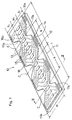
- Fig. 1 is a perspective view showing a material head embodying the present invention;
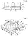
- Fig. 2 is a sectional view taken along lines II-II in Fig. 1;
- Fig. 3 is a perspective view showing a unit head obtained from the material head of Fig. 1;
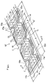
- Fig. 4 is a perspective view showing another material head embodying the present invention;
- Fig. 5 is a sectional view taken on lines V-V in Fig. 4;
- Fig. 6 is a perspective view showing a unit head obtained from the material head of Fig. 4;
- Fig. 7 is a perspective view showing a prior art divisional-type thermal head;
- Fig. 8 is a perspective view showing a unit head incorporated in the prior art divisional-type thermal head; and
- Fig. 9 is a perspective view showing how the unit head is made from a material head according to the prior art method.
- Referring first to Figs. 1 to 3 showing a first embodiment of the present invention, there is illustrated an
elongate material head 10 having an overall length L and a width W. The material head comprises aninsulating substrate 11 and aglaze layer 12 formed on the upper surface of the substrate. The glaze layer may be made of glass for example. - On the upper surface of the
glaze layer 12 is formed an array ofheating dot portions 13 arranged at suitable pitch. Each heating dot portion has a pair ofelectrodes longitudinal edges - If acceptable, the
glaze layer 12 may be omitted. In this case, the array ofheating dot portions 13 together with the associatedelectrodes insulating substrate 11. - A
protective layer 16 is further formed on the upper surface of theglaze layer 12 to cover the array ofheating dot portions 13 together with the associatedelectrodes - In manufacture of unit heads, the
material head 10 is cut transversely along cutting lines C by a suitable cutting device such as diamond cutter. The cutting lines C are spaced longitudinally of the material head, and each cutting line extends between two adjacentheating dot portions 13. As a result, the material head is divided into a plurality of unit heads A (only one shown in Fig. 3) each having a divided length s. - According to the embodiment of Figs. 1-3, the
protective layer 16 has a pair of generally V-shaped cutouts cutouts longitudinal edges protective layer 16 toward the array ofheating dot portions 13. Thus, the width of the protective layer is greatly reduced at the cutting line C. - As a result of forming the V-shaped
cutouts electrodes electrodes protective layer 16, and thecutouts - With the arrangement described above, the
protective layer 16 is made to have a reduced width W1 (see Fig. 1) at each cutting line C. If the distance from the bottom of eachcutout longitudinal edge substrate 11 is represented by X1, the reduced width W1 of the protective layer is given by W - 2(X1), wherein W represents the width of thematerial head 10. Thus, the cutting length for the protective layer is correspondingly reduced. - Obviously, the amount of chipping with respect to the
protective layer 16 is greatly reduced at the time of cutting thematerial head 10 along the respective cutting lines C. Further, theprotective layer 16 is also less liable to chipping during subsequent handling of each unit head A. - Figs. 6 to 8 show a second embodiment which utilizes another material head 10'. Similarly to the first embodiment, the material head 10' comprises an insulating
substrate 11, a glaze layer 12', and aprotective layer 16. The glaze layer 12' carries an array ofheating dot portions 13 together with their associatedelectrodes protective layer 16 has a pair ofwidth reducing cutouts protective layer 16 is given by W - 2(X1), as defined for the first embodiment. - According to the second embodiment, the glaze layer 12' also has a pair of
width reducing cutouts cutouts longitudinal edges heating dot portions 13. - If the depth of each
cutout protective layer 16, W2 is no smaller than W1 while X2 is no larger than X1. - In manufacture, the material head 10' is cut along the respective cutting lines C to provide a plurality of unit heads A' (only one shown in Fig. 6). Obviously, due to the provision of the
cutouts protective layer 16 at the time of and after cutting the material head 10'. - In the foregoing description, the term "cutout" is used only to indicate a portion where the glaze layer 12 (or 12') or the
protective layer 16 is partially absent. This term should not be limitatively understood that the glaze layer or the protective layer is "later" removed partially. - In either of the first and second embodiments, the shape of each
width reducing cutout - Further, in the drawings for the first and second embodiments, the respective reduced widths W1, W2 of the glaze layer 12 (or 12') and
protective layer 16 are shown wider than actually are. In practice, the respective reduced widths W1, W2 may be rendered as small as about 3-6mm if the width W of the material head 10 (or 10'') is 35mm for example. Thus, the chipping reduction actually obtainable by the present invention is greatly significant. - The invention being thus described, it is obvious that the same may be varied in many ways. Such variations are not to be regarded as a departure from the spirit and scope of the invention, and all such modifications as would be obvious to those skilled in the art are intended to be included within the scope of the following claims.
Claims (8)
- A method of making unit heads (A, A') for a divisional-type thermal head from a material head (10, 10'), the material head comprising an elongate insulating substrate (11) which carries a longitudinal array of heating dot portions (13) arranged at suitable pitch and pairs of electrodes (14, 15) connected to the respective dot portions, the material head further comprising a protective layer (16) extending longitudinally of the substrate to cover the array of heat dot portions and the pairs of electrodes, the method comprising dividing the material head into a plurality of unit heads (A, A') by cutting the material head along at least one cutting line (C) which extends transversely of the substrate at a position between two adjacent heating dot portions, characterized in that the protective layer (16) has a cutout (17a, 17b) which extends from at least one longitudinal edge (16a, 16b) of the protective layer toward the array of heating dot portions (13) at the position of the cutting line (C).
- The method according to claim 1, wherein the cutout (17a, 17b) is generally V-shaped.
- The method according to claim 1, wherein the electrodes (14, 15) in each unit head (A, A') are inclined toward each other as they extends away from the array of heating dot portions (13).
- The method according to claim 1, wherein the protective layer (16) has an additional cutout (17a, 17b) extending from the other longitudinal edge (16a, 16b) of the protective layer toward the array of heating dot portions (13) at the position of the cutting line (C).
- The method according to claim 1, wherein the material head further comprises a glaze layer (12, 12') formed on the substrate (11), the array of heating dot portions (13) together with the pairs of electrodes (14, 15) being formed on the glaze layer.
- The method according to claim 5, wherein the glaze layer (12') has a cutout (18a, 18b) which extends from at least one longitudinal edge (11a, 11b) of the glaze layer (12') toward the array of heating dot portions (13) at the position of the cutting line (C).
- The method according to claim 6, wherein the cutout (18a, 18b) of the glaze layer (12') is generally V-shaped.
- The method according to claim 6, wherein the glaze layer (12') has an additional cutout (18a, 18b) extending from the other longitudinal edge (11a, 11b) of the glaze layer toward the array of heating dot portions (13) at the position of the cutting line (C).
Applications Claiming Priority (4)
| Application Number | Priority Date | Filing Date | Title |
|---|---|---|---|
| JP10274391 | 1991-05-08 | ||
| JP102743/91 | 1991-05-08 | ||
| JP14985/92 | 1992-01-30 | ||
| JP4014985A JPH0542699A (en) | 1991-05-08 | 1992-01-30 | Preparation of unit thermal head in split/connection type thermal head |
Publications (2)
| Publication Number | Publication Date |
|---|---|
| EP0512251A1 true EP0512251A1 (en) | 1992-11-11 |
| EP0512251B1 EP0512251B1 (en) | 1995-03-22 |
Family
ID=26351042
Family Applications (1)
| Application Number | Title | Priority Date | Filing Date |
|---|---|---|---|
| EP92105715A Expired - Lifetime EP0512251B1 (en) | 1991-05-08 | 1992-04-02 | Method of making unit heads for divisonal-type thermal head |
Country Status (4)
| Country | Link |
|---|---|
| US (1) | US5222291A (en) |
| EP (1) | EP0512251B1 (en) |
| JP (1) | JPH0542699A (en) |
| DE (1) | DE69201749T2 (en) |
Cited By (1)
| Publication number | Priority date | Publication date | Assignee | Title |
|---|---|---|---|---|
| EP0633140A3 (en) * | 1993-07-09 | 1996-12-11 | Rohm Co Ltd | Thermal head. |
Families Citing this family (4)
| Publication number | Priority date | Publication date | Assignee | Title |
|---|---|---|---|---|
| TW309483B (en) * | 1995-10-31 | 1997-07-01 | Hewlett Packard Co | |
| US7387458B2 (en) * | 2003-08-13 | 2008-06-17 | Paxar Americas, Inc. | Printer and method of printing with a plurality of selectable registration sensors |
| JP6356539B2 (en) * | 2014-08-28 | 2018-07-11 | 京セラ株式会社 | Thermal head and thermal printer |
| JP6987588B2 (en) * | 2017-09-29 | 2022-01-05 | 京セラ株式会社 | Thermal head and thermal printer |
Citations (1)
| Publication number | Priority date | Publication date | Assignee | Title |
|---|---|---|---|---|
| FR2420272A1 (en) * | 1977-03-17 | 1979-10-12 | Oki Electric Ind Co Ltd | Multilayer printed circuit thermal printer head - has parallel grouped heating conductors covered by second set of parallel conductors making selective connections |
Family Cites Families (2)
| Publication number | Priority date | Publication date | Assignee | Title |
|---|---|---|---|---|
| JPS60157885A (en) * | 1984-01-28 | 1985-08-19 | Alps Electric Co Ltd | Thermal head manufacturing method |
| JPS6311993A (en) * | 1986-07-03 | 1988-01-19 | 松下電器産業株式会社 | dynamic display device |
-
1992
- 1992-01-30 JP JP4014985A patent/JPH0542699A/en active Pending
- 1992-04-01 US US07/861,905 patent/US5222291A/en not_active Expired - Fee Related
- 1992-04-02 EP EP92105715A patent/EP0512251B1/en not_active Expired - Lifetime
- 1992-04-02 DE DE69201749T patent/DE69201749T2/en not_active Expired - Fee Related
Patent Citations (1)
| Publication number | Priority date | Publication date | Assignee | Title |
|---|---|---|---|---|
| FR2420272A1 (en) * | 1977-03-17 | 1979-10-12 | Oki Electric Ind Co Ltd | Multilayer printed circuit thermal printer head - has parallel grouped heating conductors covered by second set of parallel conductors making selective connections |
Non-Patent Citations (2)
| Title |
|---|
| PATENT ABSTRACTS OF JAPAN vol. 6, no. 39 (M-116)(917) 10 March 1982 & JP-A-56 154 070 ( NIPPON DENKI K.K. ) 28 November 1981 * |
| PATENT ABSTRACTS OF JAPAN vol. 9, no. 322 (M-440)(2045) 18 December 1985 & JP-A-60 157 885 ( ALPS DENKI K.K. ) 19 August 1985 * |
Cited By (2)
| Publication number | Priority date | Publication date | Assignee | Title |
|---|---|---|---|---|
| EP0633140A3 (en) * | 1993-07-09 | 1996-12-11 | Rohm Co Ltd | Thermal head. |
| US5914743A (en) * | 1993-07-09 | 1999-06-22 | Rohm Co., Ltd. | Thermal head |
Also Published As
| Publication number | Publication date |
|---|---|
| DE69201749D1 (en) | 1995-04-27 |
| EP0512251B1 (en) | 1995-03-22 |
| DE69201749T2 (en) | 1995-07-27 |
| US5222291A (en) | 1993-06-29 |
| JPH0542699A (en) | 1993-02-23 |
Similar Documents
| Publication | Publication Date | Title |
|---|---|---|
| EP0414241B1 (en) | Indexable cutting insert | |
| US4968996A (en) | Thermal printhead | |
| EP0506238A3 (en) | Composite cutting insert | |
| EP0736900A3 (en) | Replacing semiconductor chips in a full-width chip array | |
| EP0512251B1 (en) | Method of making unit heads for divisonal-type thermal head | |
| US3968500A (en) | Electrode printing head and method for making the same | |
| EP0639463B1 (en) | Method of dot printing and corresponding ink jet print head | |
| US5474406A (en) | Cutting plate for a reamer | |
| JPH07299633A (en) | End mill | |
| GB2065002A (en) | Cutting tool insert with chip breaker | |
| KR100206622B1 (en) | Method of forming auxiliary electrode layer for common electrode pattern in thermal head | |
| US5373625A (en) | Method for making thermal heads | |
| JP2815787B2 (en) | Thermal head | |
| EP0174656A1 (en) | A device for cutting strip material | |
| JPH06238594A (en) | Forming notch of character font | |
| JP2578140B2 (en) | Manufacturing method of thermal head | |
| EP0053706A2 (en) | Method of manufacture multi-wire nonimpact printheads | |
| SU1191197A1 (en) | Twist drill | |
| JP4085581B2 (en) | Recording medium and manufacturing method thereof | |
| JP2001250981A (en) | Light emitting element array chip and method of manufacturing the same | |
| JPH05152611A (en) | Manufacture of led semiconductor chip for led array print head | |
| JP3033064B2 (en) | Thermal head | |
| JPS61120769A (en) | Edge type thermal head | |
| JPH0220437B2 (en) | ||
| EP0628416A1 (en) | End-contact type thermal head and manufacturing method therefor |
Legal Events
| Date | Code | Title | Description |
|---|---|---|---|
| PUAI | Public reference made under article 153(3) epc to a published international application that has entered the european phase |
Free format text: ORIGINAL CODE: 0009012 |
|
| AK | Designated contracting states |
Kind code of ref document: A1 Designated state(s): DE FR GB |
|
| 17P | Request for examination filed |
Effective date: 19930217 |
|
| 17Q | First examination report despatched |
Effective date: 19940607 |
|
| GRAA | (expected) grant |
Free format text: ORIGINAL CODE: 0009210 |
|
| AK | Designated contracting states |
Kind code of ref document: B1 Designated state(s): DE FR GB |
|
| REF | Corresponds to: |
Ref document number: 69201749 Country of ref document: DE Date of ref document: 19950427 |
|
| ET | Fr: translation filed | ||
| PLBE | No opposition filed within time limit |
Free format text: ORIGINAL CODE: 0009261 |
|
| STAA | Information on the status of an ep patent application or granted ep patent |
Free format text: STATUS: NO OPPOSITION FILED WITHIN TIME LIMIT |
|
| 26N | No opposition filed | ||
| PGFP | Annual fee paid to national office [announced via postgrant information from national office to epo] |
Ref country code: GB Payment date: 20000329 Year of fee payment: 9 |
|
| PGFP | Annual fee paid to national office [announced via postgrant information from national office to epo] |
Ref country code: DE Payment date: 20000403 Year of fee payment: 9 |
|
| PGFP | Annual fee paid to national office [announced via postgrant information from national office to epo] |
Ref country code: FR Payment date: 20000411 Year of fee payment: 9 |
|
| PG25 | Lapsed in a contracting state [announced via postgrant information from national office to epo] |
Ref country code: GB Free format text: LAPSE BECAUSE OF NON-PAYMENT OF DUE FEES Effective date: 20010402 |
|
| PG25 | Lapsed in a contracting state [announced via postgrant information from national office to epo] |
Ref country code: FR Free format text: THE PATENT HAS BEEN ANNULLED BY A DECISION OF A NATIONAL AUTHORITY Effective date: 20010430 |
|
| GBPC | Gb: european patent ceased through non-payment of renewal fee |
Effective date: 20010402 |
|
| PG25 | Lapsed in a contracting state [announced via postgrant information from national office to epo] |
Ref country code: DE Free format text: LAPSE BECAUSE OF NON-PAYMENT OF DUE FEES Effective date: 20020201 |
|
| REG | Reference to a national code |
Ref country code: FR Ref legal event code: ST |