EP0511014B1 - Integrally molded printed circuit board and method of making the same - Google Patents
Integrally molded printed circuit board and method of making the same Download PDFInfo
- Publication number
- EP0511014B1 EP0511014B1 EP19920303738 EP92303738A EP0511014B1 EP 0511014 B1 EP0511014 B1 EP 0511014B1 EP 19920303738 EP19920303738 EP 19920303738 EP 92303738 A EP92303738 A EP 92303738A EP 0511014 B1 EP0511014 B1 EP 0511014B1
- Authority
- EP
- European Patent Office
- Prior art keywords
- circuit board
- enclosure
- printed circuit
- assembly
- mechanical locking
- Prior art date
- Legal status (The legal status is an assumption and is not a legal conclusion. Google has not performed a legal analysis and makes no representation as to the accuracy of the status listed.)
- Expired - Lifetime
Links
Images


Classifications
-
- B—PERFORMING OPERATIONS; TRANSPORTING
- B29—WORKING OF PLASTICS; WORKING OF SUBSTANCES IN A PLASTIC STATE IN GENERAL
- B29C—SHAPING OR JOINING OF PLASTICS; SHAPING OF MATERIAL IN A PLASTIC STATE, NOT OTHERWISE PROVIDED FOR; AFTER-TREATMENT OF THE SHAPED PRODUCTS, e.g. REPAIRING
- B29C45/00—Injection moulding, i.e. forcing the required volume of moulding material through a nozzle into a closed mould; Apparatus therefor
- B29C45/14—Injection moulding, i.e. forcing the required volume of moulding material through a nozzle into a closed mould; Apparatus therefor incorporating preformed parts or layers, e.g. injection moulding around inserts or for coating articles
- B29C45/14639—Injection moulding, i.e. forcing the required volume of moulding material through a nozzle into a closed mould; Apparatus therefor incorporating preformed parts or layers, e.g. injection moulding around inserts or for coating articles for obtaining an insulating effect, e.g. for electrical components
-
- B—PERFORMING OPERATIONS; TRANSPORTING
- B29—WORKING OF PLASTICS; WORKING OF SUBSTANCES IN A PLASTIC STATE IN GENERAL
- B29C—SHAPING OR JOINING OF PLASTICS; SHAPING OF MATERIAL IN A PLASTIC STATE, NOT OTHERWISE PROVIDED FOR; AFTER-TREATMENT OF THE SHAPED PRODUCTS, e.g. REPAIRING
- B29C37/00—Component parts, details, accessories or auxiliary operations, not covered by group B29C33/00 or B29C35/00
- B29C37/0078—Measures or configurations for obtaining anchoring effects in the contact areas between layers
- B29C37/0082—Mechanical anchoring
-
- B—PERFORMING OPERATIONS; TRANSPORTING
- B29—WORKING OF PLASTICS; WORKING OF SUBSTANCES IN A PLASTIC STATE IN GENERAL
- B29C—SHAPING OR JOINING OF PLASTICS; SHAPING OF MATERIAL IN A PLASTIC STATE, NOT OTHERWISE PROVIDED FOR; AFTER-TREATMENT OF THE SHAPED PRODUCTS, e.g. REPAIRING
- B29C70/00—Shaping composites, i.e. plastics material comprising reinforcements, fillers or preformed parts, e.g. inserts
- B29C70/68—Shaping composites, i.e. plastics material comprising reinforcements, fillers or preformed parts, e.g. inserts by incorporating or moulding on preformed parts, e.g. inserts or layers, e.g. foam blocks
-
- H—ELECTRICITY
- H05—ELECTRIC TECHNIQUES NOT OTHERWISE PROVIDED FOR
- H05K—PRINTED CIRCUITS; CASINGS OR CONSTRUCTIONAL DETAILS OF ELECTRIC APPARATUS; MANUFACTURE OF ASSEMBLAGES OF ELECTRICAL COMPONENTS
- H05K3/00—Apparatus or processes for manufacturing printed circuits
- H05K3/0011—Working of insulating substrates or insulating layers
- H05K3/0014—Shaping of the substrate, e.g. by moulding
-
- H—ELECTRICITY
- H05—ELECTRIC TECHNIQUES NOT OTHERWISE PROVIDED FOR
- H05K—PRINTED CIRCUITS; CASINGS OR CONSTRUCTIONAL DETAILS OF ELECTRIC APPARATUS; MANUFACTURE OF ASSEMBLAGES OF ELECTRICAL COMPONENTS
- H05K7/00—Constructional details common to different types of electric apparatus
- H05K7/14—Mounting supporting structure in casing or on frame or rack
- H05K7/1417—Mounting supporting structure in casing or on frame or rack having securing means for mounting boards, plates or wiring boards
-
- B—PERFORMING OPERATIONS; TRANSPORTING
- B29—WORKING OF PLASTICS; WORKING OF SUBSTANCES IN A PLASTIC STATE IN GENERAL
- B29L—INDEXING SCHEME ASSOCIATED WITH SUBCLASS B29C, RELATING TO PARTICULAR ARTICLES
- B29L2031/00—Other particular articles
- B29L2031/34—Electrical apparatus, e.g. sparking plugs or parts thereof
- B29L2031/3481—Housings or casings incorporating or embedding electric or electronic elements
-
- H—ELECTRICITY
- H05—ELECTRIC TECHNIQUES NOT OTHERWISE PROVIDED FOR
- H05K—PRINTED CIRCUITS; CASINGS OR CONSTRUCTIONAL DETAILS OF ELECTRIC APPARATUS; MANUFACTURE OF ASSEMBLAGES OF ELECTRICAL COMPONENTS
- H05K2203/00—Indexing scheme relating to apparatus or processes for manufacturing printed circuits covered by H05K3/00
- H05K2203/13—Moulding and encapsulation; Deposition techniques; Protective layers
- H05K2203/1305—Moulding and encapsulation
- H05K2203/1327—Moulding over PCB locally or completely
Definitions
- the present invention relates to a method of integrally molding a printed circuit board to an enclosure by the use of injection molding and the resulting product.
- Printed circuit boards also known as printed circuit boards, are conventionally mounted in enclosures with the use of screws, snaps, or other mechanical securing means.
- the additional space occupied by the mechanical securing means did not pose a problem since the overall size of the structure was dictated more by the size of the electrical components mounted on the wiring board rather than by the space occupied by the mechanical mounting means.
- the space consumed by mechanical attaching means has become a significant portion of the total overall dimensions of the device, in particular the thickness of the device.
- the enclosure must contain material having the suitable thickness to provide a substantial amount of material into which the screw may be inserted to hold the printed circuit board in place.
- Mechanical means including snaps, fasteners and the like also require a comparatively substantial thickness or volume in the enclosure to hold the associated mechanical latching means.
- the use of adhesives, glues and the like have not been successfully used for several important reasons.
- the enclosures into which the printed circuit boards are mounted are made of thermoplastic resins which have a substantially different thermal expansion coefficient than does the printed circuit board which is typically manufactured of a thermoset resin or glass filled resin and is specifically designed not to have a substantial coefficient of thermal expansion.
- the use of glues to attach printed circuit boards has not been successful since with the repeated expansion and contraction of the container through varying temperature cycles, the adhesive bond between the printed circuit board and the container is destroyed.
- for the use of adhesive requires that the adhesive be applied across the entire face of a printed circuit board and not merely at the edges.
- FIG. 15 numeral 190 is the box body, in this instance a meter housing, item 290 is the printed circuit board which is integrally molded on the rear surface of the box body, and 390 represents a conductor circuit pattern formed on the surface of the printed circuit board 290.
- the technique of the Japanese Utility Model suffers from several important deficiencies. First, it provides for only one surface of the printed circuit board to carry active electronic devices thereby precluding the use of both major surfaces for active devices. Second, the technique of the Japanese Utility Model has not proven successful since the printed circuit board can over time become loosened or detached from the box body.
- the box body is manufactured of a thermoplastic resin which has a different thermal coefficient of expansion than does the circuit board. That is, the box body will expand or shrink to a much greater degree with changes in temperature than will the printed circuit board. So long as the temperature to which the box body is exposed does not vary significantly, the printed circuit board should remain tightly held in place. However, if the box body is exposed to significant temperature fluctuation such as from 0 to 35°C, then the printed circuit board could become detached from the box body as a result of the temperature fluctuations, especially at the high temperatures where the box body will expand substantially more than the printed circuit board thus offering the possibility of release of the printed circuit board from the box body.
- thermoset printed circuit board it is a further objective of the present invention to provide for a method of permanently assembling a thermoset printed circuit board to a container made of thermoplastic resin.
- a method of assembling a printed circuit board to an enclosure by the steps of positioning a printed circuit board in a mold, injection molding plastic resin into the mold to form an enclosure, wherein the circuit board is configured such that plastic flow during the injection molding step creates a mechanical locking engagement between the circuit board and the enclosure during the injection molding step, and removing the assembled circuit board and enclosure from the mold.
- At least a portion of the periphery of the circuit board is bevelled to form the mechanical locking engagement.
- the mechanical locking engagement is formed by at least a portion of the periphery of the circuit board being fitted in a groove of the enclosure by a depth greater than a maximum expected difference in thermal expansion between the enclosure and the circuit board.
- the circuit board has reversed notches into which the plastic flows to form the mechanical locking engagement.
- mold pieces are positioned against the circuit board in the mold such that openings for access to the circuit board are formed in the enclosure.
- the circuit board has holes into which plastic flows during the injection molding step to form the mechanical locking engagement.
- reinforcing ribs are formed in the enclosure during the molding step for reinforcing the circuit board.
- the present invention is further carried out by an assembly of a circuit board and an enclosure, comprising a circuit board and a molded plastic enclosure molded to the circuit board.
- the circuit board and the enclosure have portions configured such that a mechanical locking engagement is formed between the circuit board and the enclosure during the molding of the enclosure.
- the invention also provides an assembly as set out in Claim 17 or 18.
- the enclosure typically is formed of at least two parts, a lower case and an upper case which are joined together to produce the assembled electronic device such as cellular telephone or the like.
- the upper case is designated with the numeral 2 and the lower case with the numeral 1.
- the printed circuit boards are shown as items 14 and 15 with the electronic parts generally designated by the numeral 4 while item 17 is a cover which could contain the input means for the device such as a keyboard or the like, or could simply be a protective cover.
- Items 16 represent connectors for electrically connecting the wiring boards or printed circuit boards 14 and 15 together and are shown for illustrative purposes only.
- the upper and lower cases 1 and 2 tend to expand or contract with temperature changes to a significantly greater extent than will the generally temperature stable printed circuit boards. Thus, when exposed to elevated temperatures above room temperature during use, the two cases will tend to expand or pull away from the two circuit boards. In the case of circuit board 14, one or more edges of the circuit board could become completely loosened from the case if thermal expansion was sufficient that the case expanded to a greater extent than the depth d shown on Figure 4.
- case 1 would be formed around circuit board 14 to a sufficient depth such that during the normal temperature cycle the total expansion of the case in either its width or its length would the less than the distance "d" shown in Figure 4. In this manner, a strong mechanical connection can be formed between the case and the printed circuit board.
- the edge of the printed circuit board should be formed such that the face of the board containing the active electronic components, i.e., the top, has a smaller surface area than the back surface of the printed circuit board which is embedded in the plastic.
- the circuit board will be retained in the case by a mechanical connection at the corresponding bevelled edges of the case 2, even when the case undergoes thermal expansion, so long as the distance "d" shown on Figure 6 is greater than the linear expansion of the case in either the length or width directions. Since the length of the box is generally greater than the width of the box, the "d" dimension in the length direction should be greater than that in the width direction.
- the necessary depth “d” is readily calculated by utilizing the thermal coefficients of expansion for both the board and the case material.
- the "d" dimension should be at least as great as the difference between the thermal expansions of the two materials over the full extent of the temperature range to which the device is expected to be exposed to or designed to withstand.
- FIG. 10 The conventional prior art techniques of attaching the wiring board through the use of screws or the like is illustrated in Figure 10.
- the structure necessary to accommodate the screws results in a substantially thicker case than does the structure illustrated in Figure 1.
- numeral 91 represents the lower case and numeral 92 the upper case and openings 92a and 91a represent openings in the structure itself to accommodate devices such as switches 911 of LEDs 98.
- Item 912 is the mounting means for the switch on the inside of the case and element 99 is the mounting means for the LED also on the inside of the case.
- the screws 95 mount the two circuit boards 93 and 96 with active elements 94 thereon to the lower case 91. Connection between the two circuit boards is shown at 97 while connections to the various active devices mounted on the walls of the case are shown as 913 and 910 respectively. As can be seen in this device, a substantial amount of space is necessary to accommodate the separate elements.
- Figures 7 and 8 With the present technique it would be possible to directly mount both the switch and the diode on the printed circuit board 15 with openings 2b and 2c through the case 2 to provide the necessary access.
- the use of separate wiring leads and attachment means for both the diodes and switches as in conventional devices is avoided by the direct connection to the printed circuit board.
- Figure 8 shows an expanded view of Figure 7.
- the numerals correspond to the same parts as in Figure 1 with 2c representing the openings for the active devices 8 and 11, 8 for example being an LED and 11 a volume control switch.
- the arrangement in accordance with the present invention is far more compact than one according to the prior art as illustrated in Figure 10.
- FIG 9 illustrates yet another possible embodiment of the present invention.
- circuit boards are located not only on the major faces of the device but also in the sides, as evidenced by circuit boards 20 and 21 in addition to wiring board 18.
- circuit boards 20 and 21 in addition to wiring board 18.
- circuit boards 20 and 21 in addition to wiring board 18.
- essentially all surfaces of the case will contain circuit boards.
- the walls into which the circuit boards are inserted must be comparatively thick to accommodate the results of thermal expansion and to provide the necessary strength to the case. Where it is desired to make the walls as thin as possible or to mount the circuit boards not in a major face of the case, but rather than in the middle, this would result in a thickening of the wall structure such that the minimum case size would not be achieved.
- Figure 13 illustrates a solution to this problem.
- the circuit board is provided with reverse taper openings or notches, i.e., these which are wider in the interior of the board than at the edge of the board.
- the edges of the board 15 having circuit elements 13 have opening 15b of trapezoidal shapes, however circular shapes or triangular shapes where the base of the triangle is located within the board and the apex towards the exterior of the board, or circular openings where the diameter of the circular opening lies within the body of the printed circuit board, may instead be used.
- the walls need not be thick to restrain the board in the event of expansion or contraction but rather the flow of the plastic into the shaped openings during molding effectively locks the circuit board in place such that the walls of the device may remain thin throughout the major portion of the case and the board is locked in place.
- the notches 15b form a mechanical locking of the printed circuit board with correspondingly shaped elements in the sides of the case.
- the plastic within the notches 15b restrains the printed circuit board in place, and even though the case has tended to move away from the board, the presence of plastic within the notches 15b acts as a mechanical lock on the board.
- the number of notches or size of notches used is not important so long as the stress imposed by the thermal expansion of the box does not exceed the strength of the plastic at the narrowest most portion or neck of the notch. Overstressing of the plastic could cause the plastic over time to undergo fatigue failure.
- Figure 14 is an alternative technique for mechanically locking the printed circuit board onto a major surface of the case.
- the case 1 has openings for active devices 140 while other active devices 130 are on the opposite side of the board 15 having circuit pattern 5 facing inward.
- the conductor circuit pattern 6 may be buried within the thermoplastic forming the case even though it generally is not desirable to incorporate active devices within the thermoplastic resin.
- holes 15c have been drilled into the circuit board through which the plastic forming the case may flow during molding to form a pin having a flattened head. In this way, the pins formed in place serve to hold the circuit board in place even when undergoing thermal expansion.
- Figure 11 illustrates the method by which one would form by injection molding the case around a printed circuit board
- Figure 12 illustrates the finished device.
- item 1 represents the container or box to hold the printed circuit board
- item 15 is the printed circuit board itself
- 15b is the bevel or tapered portion of the periphery the printed circuit board which serves to form the mechanical correction with the enclosure.
- Items 5 and 6 are the conductor circuit patterns on the board and items 130 and 140 are active electronic components.
- Item 12 is the open space into which the plastic will be injected typically through opening 110 in die 100.
- Item 7 is the corresponding die which has a top 80 and notches 7a around the conductor patterns 6 and 5 formed on the printed circuit board.
- Item 9 having notches 9a is shown as separate pieces, but may be integral with die 100.
- the printed circuit board When the printed circuit board is not mounted against a major face of the case but is rather suspended from the side walls of the case, as illustrated in Figure 16, the printed circuit board may, prior to being mounted in the case be fully wired with the active devices are then joined to the case by the injection molding procedure. This procedure can be accomplished using conventional techniques.
- the advantage of this particular embodiment is ease of assembly since the printed circuit board may be fully assembled before being mounted into the case. A view of this is shown in Figure 16A illustrating a printed circuit board which has been mounted into the middle of a case rather than into either the top of the bottom.
- element 20A is a stiffening rib which is molded at the same time as case 1 is molded around printed circuit board 15.
- the openings in the printed circuit board are of a general circular shape as shown in 15d and it is the injection molding of plastic into these openings during the formation of the case that locks the printed circuit board into place.
- element 21 is a portion of the case which does not contain any printed circuit board elements. This may be either an opening or an injection molded surface onto which other devices are mounted, such as speakers or the like.
- Figure 16A is a sectional view along line AA of Figure 16.
- the printed circuit board 15 extends only partway in the side walls of the case.
- the depth to which the printed circuit board extends into the case need only be sufficient to allow the flow of plastic during injection molded into the openings 15a.
- rib 20A is bonded not only to the side case 1 but also to the printed circuit board 15 as a result of printed circuit board 15 containing openings through which the plastic forming the rib can flow in the form of pins, shown as 20a, such that the rib will perform a stiffening function with respect to the printed circuit board as well as protect the printed circuit board from deflection as by the overlying top of the case (not shown).
- pins 20a are shown as extending completely through and protruding beyond the lowest surface of the printed circuit board, they need not extend fully through the printed circuit board.
- the openings in the printed circuit board at which cooperate with the case to mechanically restrain the printed circuit board in place may have either bevelled or unbevelled edges. That is, the top and bottom of these openings may be wider than the center portion in the printed circuit board.
- the embodiment of Figure 16 can be readily manufactured using conventional injection molding techniques.
- the printed circuit board would be inserted into the mold used to form the case 1 in a fashion such that openings 15a were disposed within the die such that the thermoplastic resin comprising the case could flow during the forming process into the openings.
- the reverse side which is generally smooth can function as one surface of a battery compartment thereby further decreasing the size of the device. This would find particular use in hand held calculators, cellular telephones and the like.
- the thermoplastic resin which forms the case can be essentially any thermoplastic resin which may be molded. While essentially any thermoplastic resin may be used, it is generally preferable to use the so-called engineering plastics which tend to have excellent impact strengths and dimensional stability such as polybutylenetelephtalate (PBT) or polyphenylenesulfide (PPS). This results in a case which can withstand the substantial amount of abuse that many portable electronic components are subjected to including accidental dropping, exposure to moisture and the like.
- PBT polybutylenetelephtalate
- PPS polyphenylenesulfide
- the printed circuit boards are conventionally made from glass and impregnated resins, thermoset resins and combinations thereof. Essentially any printed circuit board may be mounted in accordance with the present technique.
- Engineering plastics which may be used include hybrid heat resistant resin (HHR), heat resistant glass fiber based epoxy resins such as FR-4, polyphenylene sulfide, high impact polystyrenes, polycarbonates, syndiotactic polystyrenes and the like.
- HHR hybrid heat resistant resin
- FR-4 heat resistant glass fiber based epoxy resins
- polyphenylene sulfide high impact polystyrenes
- polycarbonates such as polycarbonates
- syndiotactic polystyrenes such as polypropylene, polyethylene, may also be used if desired.
- Other non-engineering thermoplastic resins such as polypropylene, polyethylene, may also be used if desired.
- the casing may, for example, be 100mm x 150mm x 20mm.
- Exemplary molding conditions may be:
- the present invention offers a substantial advantage over screws which, as a result of exposure to normal vibratory forces, after extended periods of time may become loose allowing the printed circuit board to move causing failure of the device.
Landscapes
- Engineering & Computer Science (AREA)
- Mechanical Engineering (AREA)
- Manufacturing & Machinery (AREA)
- Microelectronics & Electronic Packaging (AREA)
- Chemical & Material Sciences (AREA)
- Composite Materials (AREA)
- Casings For Electric Apparatus (AREA)
Description
- The present invention relates to a method of integrally molding a printed circuit board to an enclosure by the use of injection molding and the resulting product.
- Printed circuit boards, also known as printed circuit boards, are conventionally mounted in enclosures with the use of screws, snaps, or other mechanical securing means. Until recently, the additional space occupied by the mechanical securing means did not pose a problem since the overall size of the structure was dictated more by the size of the electrical components mounted on the wiring board rather than by the space occupied by the mechanical mounting means. However, with the increasing miniaturization of electronics and the desire to manufacture smaller and smaller electronic devices to improve portability, the space consumed by mechanical attaching means has become a significant portion of the total overall dimensions of the device, in particular the thickness of the device. If the mechanical mounting means such as screws are used, then the enclosure must contain material having the suitable thickness to provide a substantial amount of material into which the screw may be inserted to hold the printed circuit board in place. Mechanical means including snaps, fasteners and the like also require a comparatively substantial thickness or volume in the enclosure to hold the associated mechanical latching means.
- The use of adhesives, glues and the like have not been successfully used for several important reasons. First, in most instances the enclosures into which the printed circuit boards are mounted are made of thermoplastic resins which have a substantially different thermal expansion coefficient than does the printed circuit board which is typically manufactured of a thermoset resin or glass filled resin and is specifically designed not to have a substantial coefficient of thermal expansion. As a result of the mismatch between the coefficients of thermal expansion between the printed circuit board and the enclosure, the use of glues to attach printed circuit boards has not been successful since with the repeated expansion and contraction of the container through varying temperature cycles, the adhesive bond between the printed circuit board and the container is destroyed. Also, for the use of adhesive requires that the adhesive be applied across the entire face of a printed circuit board and not merely at the edges. This means that only one side of the printed circuit board can be used to mount electronic devices. It also means the printed circuit board can only be counted against a major surface of the container and can not be glued along the edges of the board and to the sides of a container. This precludes the use of both major surfaces of the printed circuit board from containing active electronic devices. It has become core and more conventional today to mount active devices on both surfaces of the printed circuit board so as to minimize overall container volume.
- In Japanese Utility Model Publication 112085/1989 there has been suggested molding of the printed circuit board into a container as illustrated in Figure 15. In Figure 5,
numeral 190 is the box body, in this instance a meter housing,item 290 is the printed circuit board which is integrally molded on the rear surface of the box body, and 390 represents a conductor circuit pattern formed on the surface of the printedcircuit board 290. The technique of the Japanese Utility Model suffers from several important deficiencies. First, it provides for only one surface of the printed circuit board to carry active electronic devices thereby precluding the use of both major surfaces for active devices. Second, the technique of the Japanese Utility Model has not proven successful since the printed circuit board can over time become loosened or detached from the box body. The box body is manufactured of a thermoplastic resin which has a different thermal coefficient of expansion than does the circuit board. That is, the box body will expand or shrink to a much greater degree with changes in temperature than will the printed circuit board. So long as the temperature to which the box body is exposed does not vary significantly, the printed circuit board should remain tightly held in place. However, if the box body is exposed to significant temperature fluctuation such as from 0 to 35°C, then the printed circuit board could become detached from the box body as a result of the temperature fluctuations, especially at the high temperatures where the box body will expand substantially more than the printed circuit board thus offering the possibility of release of the printed circuit board from the box body. - Accordingly, there remains a need for a method of firmly attaching a printed circuit board to a container without the use of mechanical fasteners, bonding agent such as adhesives wherein it is possible to mount the board such that both surfaces may be used,to,mount active devices.
- It is an object of the present invention to provide a reliable method of integrally molding a printed circuit board into a container in which both surfaces of the board may be utilized for mounting active electronic components.
- It is a further objective of the present invention to provide for a method of permanently assembling a thermoset printed circuit board to a container made of thermoplastic resin.
- It is another object of the present invention to provide a technique for bonding printed circuit boards to containers or portions thereof trough the use of injection molding techniques.
- It is yet another object of the invention to provide a method of assembling a printed circuit board to an enclosure such that a mechanical connection is formed between the circuit board and the enclosure during the molding of the enclosure.
- It is yet a further object of the invention to provide an assembly of a printed circuit board and an enclosure connected by a mechanical connection formed during the molding of the enclosure.
- The above, and other, objects are achieved according to an aspect of the present invention by a method of assembling a printed circuit board to an enclosure by the steps of positioning a printed circuit board in a mold, injection molding plastic resin into the mold to form an enclosure, wherein the circuit board is configured such that plastic flow during the injection molding step creates a mechanical locking engagement between the circuit board and the enclosure during the injection molding step, and removing the assembled circuit board and enclosure from the mold.
- According to a further feature of the invention, at least a portion of the periphery of the circuit board is bevelled to form the mechanical locking engagement.
- According to yet a further feature of the invention, the mechanical locking engagement is formed by at least a portion of the periphery of the circuit board being fitted in a groove of the enclosure by a depth greater than a maximum expected difference in thermal expansion between the enclosure and the circuit board.
- According to yet a further feature of the invention, the circuit board has reversed notches into which the plastic flows to form the mechanical locking engagement.
- According to yet a further feature of the invention, mold pieces are positioned against the circuit board in the mold such that openings for access to the circuit board are formed in the enclosure.
- According to yet a further feature of the invention, the circuit board has holes into which plastic flows during the injection molding step to form the mechanical locking engagement.
- According to yet a further feature of the invention, reinforcing ribs are formed in the enclosure during the molding step for reinforcing the circuit board.
- The present invention is further carried out by an assembly of a circuit board and an enclosure, comprising a circuit board and a molded plastic enclosure molded to the circuit board. The circuit board and the enclosure have portions configured such that a mechanical locking engagement is formed between the circuit board and the enclosure during the molding of the enclosure.
- The invention also provides an assembly as set out in
Claim - A more complete appreciation of the invention and many of the attendant advantages thereof will be readily obtained as the same becomes better understood by reference to the following detailed description when considered in connection with the accompanying drawings, wherein:
- Figure 1 is a schematic sectional view of an assembly of two circuit boards in an enclosure in accordance with the present invention;
- Figure 2 is a sectional view of a lower case of the enclosure supporting a circuit board;
- Figure 3 corresponds to Figure 2 but shows electronic elements counted on the circuit board;
- Figure 4 is a detail of a portion of the lower case at the mechanical connection between the enclosure and the circuit board, showing the depth of the groove into which the periphery of the circuit board fits;
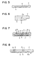
- Figure 5 corresponds to Figure 3 but shows an upper case supporting a circuit board having electronic elements thereon;
- Figure 6 is a partial sectional view of a variant of an upper case;
- Figure 7 corresponds to Figure 1 but shows another embodiment in which the upper case has openings for access to one of the circuit boards;
- Figure 8 corresponds to Figure 6 but shows a circuit board mounted in the upper case in which the upper case has openings for access to the circuit board mounted therein;
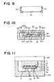
- Figure 9 shows another embodiment in which plural circuit boards are mounted at different surfaces of a case;
- Figure 10 shows a prior art assembly of a circuit board and an enclosure;
- Figure 11 shows a circuit board mounted in a mold in preparation for the molding of the enclosure;
- Figure 12 shows a circuit board having molded thereto an enclosure formed in the mold of Figure 11;
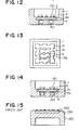
- Figure 13 shows a plan view of a further embodiment in which reverse taper notches in the periphery of the circuit board are filled with molded plastic material of the enclosure to form a mechanical connection;
- Figure 14 shows a sectional view of a further embodiment in which holes in the circuit board are filled with molded plastic material to form a mechanical connection;
- Figure 15 is a sectional view of a further prior art assembly;
- Figure 16 is a plan view of yet a further embodiment in which the circuit board has holes for the mechanical connection and the enclosure has a reinforcing rib; and
- Figure 16 A is a sectional view taken along line A-A of Figure 16.
- The box or container into which the printed circuit board is to be counted by injection molding the box or container around the printed circuit board will tend to have a greater thermal coefficient of thermal expansion than the board itself. Referring to figures 1-4, a description of the phenomenon which occurs as a result of thermal expansion will be given. the enclosure typically is formed of at least two parts, a lower case and an upper case which are joined together to produce the assembled electronic device such as cellular telephone or the like. In Figure 1 the upper case is designated with the
numeral 2 and the lower case with the numeral 1. The printed circuit boards are shown asitems numeral 4 whileitem 17 is a cover which could contain the input means for the device such as a keyboard or the like, or could simply be a protective cover. -
Items 16 represent connectors for electrically connecting the wiring boards or printedcircuit boards lower cases 1 and 2 tend to expand or contract with temperature changes to a significantly greater extent than will the generally temperature stable printed circuit boards. Thus, when exposed to elevated temperatures above room temperature during use, the two cases will tend to expand or pull away from the two circuit boards. In the case ofcircuit board 14, one or more edges of the circuit board could become completely loosened from the case if thermal expansion was sufficient that the case expanded to a greater extent than the depth d shown on Figure 4. - In the present invention this can be obviated during the molding process by designing the case such that the printed circuit board extends into each side of the case a distance greater than the total thermal expansion of the case over its expected temperature cycle. That is, in Figure 4, case 1 would be formed around
circuit board 14 to a sufficient depth such that during the normal temperature cycle the total expansion of the case in either its width or its length would the less than the distance "d" shown in Figure 4. In this manner, a strong mechanical connection can be formed between the case and the printed circuit board. - With respect to the printed
circuit board 15, as shown in Figure 6 the edge of the printed circuit board should be formed such that the face of the board containing the active electronic components, i.e., the top, has a smaller surface area than the back surface of the printed circuit board which is embedded in the plastic. By forming thebevelled edges 15a, the circuit board will be retained in the case by a mechanical connection at the corresponding bevelled edges of thecase 2, even when the case undergoes thermal expansion, so long as the distance "d" shown on Figure 6 is greater than the linear expansion of the case in either the length or width directions. Since the length of the box is generally greater than the width of the box, the "d" dimension in the length direction should be greater than that in the width direction. The necessary depth "d" is readily calculated by utilizing the thermal coefficients of expansion for both the board and the case material. The "d" dimension should be at least as great as the difference between the thermal expansions of the two materials over the full extent of the temperature range to which the device is expected to be exposed to or designed to withstand. - The approach illustrated in Figures 1-4 is useful only where the wall thickness of the case is sufficiently substantial that the insertion of the printed circuit board into the wall will not result in excessive weakening of the wall structure. As illustrated in Figure 1, this technique finds applicability when the circuit board is to be inserted at a location where the case essentially terminates at a major surface. Using this technique, the case when the upper and lower halves are assembled is much thinner than with the prior art device.
- The conventional prior art techniques of attaching the wiring board through the use of screws or the like is illustrated in Figure 10. As can be seen in Figure 10, the structure necessary to accommodate the screws results in a substantially thicker case than does the structure illustrated in Figure 1. In Figure 10, numeral 91 represents the lower case and numeral 92 the upper case and
openings 92a and 91a represent openings in the structure itself to accommodate devices such asswitches 911 ofLEDs 98.Item 912 is the mounting means for the switch on the inside of the case andelement 99 is the mounting means for the LED also on the inside of the case. Thescrews 95 mount the twocircuit boards active elements 94 thereon to thelower case 91. Connection between the two circuit boards is shown at 97 while connections to the various active devices mounted on the walls of the case are shown as 913 and 910 respectively. As can be seen in this device, a substantial amount of space is necessary to accommodate the separate elements. - In contrast, as illustrated in Figures 7 and 8 with the present technique it would be possible to directly mount both the switch and the diode on the printed
circuit board 15 withopenings case 2 to provide the necessary access. The use of separate wiring leads and attachment means for both the diodes and switches as in conventional devices is avoided by the direct connection to the printed circuit board. Figure 8 shows an expanded view of Figure 7. The numerals correspond to the same parts as in Figure 1 with 2c representing the openings for theactive devices - Figure 9 illustrates yet another possible embodiment of the present invention. In this embodiment, circuit boards are located not only on the major faces of the device but also in the sides, as evidenced by
circuit boards board 18. In this embodiment essentially all surfaces of the case will contain circuit boards. - As can be seen from the figures, the walls into which the circuit boards are inserted must be comparatively thick to accommodate the results of thermal expansion and to provide the necessary strength to the case. Where it is desired to make the walls as thin as possible or to mount the circuit boards not in a major face of the case, but rather than in the middle, this would result in a thickening of the wall structure such that the minimum case size would not be achieved. Figure 13 illustrates a solution to this problem. In this case, the circuit board is provided with reverse taper openings or notches, i.e., these which are wider in the interior of the board than at the edge of the board.
- In Figure 13 the edges of the
board 15 having circuit elements 13 have opening 15b of trapezoidal shapes, however circular shapes or triangular shapes where the base of the triangle is located within the board and the apex towards the exterior of the board, or circular openings where the diameter of the circular opening lies within the body of the printed circuit board, may instead be used. In these instances, the walls need not be thick to restrain the board in the event of expansion or contraction but rather the flow of the plastic into the shaped openings during molding effectively locks the circuit board in place such that the walls of the device may remain thin throughout the major portion of the case and the board is locked in place. - The
notches 15b form a mechanical locking of the printed circuit board with correspondingly shaped elements in the sides of the case. Thus, if the case expands as the result of thermal expansion, the plastic within thenotches 15b restrains the printed circuit board in place, and even though the case has tended to move away from the board, the presence of plastic within thenotches 15b acts as a mechanical lock on the board. The number of notches or size of notches used is not important so long as the stress imposed by the thermal expansion of the box does not exceed the strength of the plastic at the narrowest most portion or neck of the notch. Overstressing of the plastic could cause the plastic over time to undergo fatigue failure. This can be avoided by either making the neck fairly wide as illustrated in Figure in or by providing a large number of notches along the length and width of the printed circuit board. The number of notches necessary is determined by the neck size and the expected degree of thermal expansion. The shape and size of the notch is not critical so long as it is of size and shape such that it will lock the printed circuit board in place. - Figure 14 is an alternative technique for mechanically locking the printed circuit board onto a major surface of the case. As illustrated in Figure 14, the case 1 has openings for
active devices 140 while otheractive devices 130 are on the opposite side of theboard 15 havingcircuit pattern 5 facing inward. As is illustrated, theconductor circuit pattern 6 may be buried within the thermoplastic forming the case even though it generally is not desirable to incorporate active devices within the thermoplastic resin. In this instance, holes 15c have been drilled into the circuit board through which the plastic forming the case may flow during molding to form a pin having a flattened head. In this way, the pins formed in place serve to hold the circuit board in place even when undergoing thermal expansion. - Figure 11 illustrates the method by which one would form by injection molding the case around a printed circuit board and Figure 12 illustrates the finished device. In these figures, item 1 represents the container or box to hold the printed circuit board,
item 15 is the printed circuit board itself, 15b is the bevel or tapered portion of the periphery the printed circuit board which serves to form the mechanical correction with the enclosure.Items items Item 12 is the open space into which the plastic will be injected typically throughopening 110 indie 100.Item 7 is the corresponding die which has a top 80 andnotches 7a around theconductor patterns Item 9 havingnotches 9a is shown as separate pieces, but may be integral withdie 100. It forms molds around which the plastic will be injected to form theopenings active devices 140 can be accessed from the exterior or the box or form openings into which they will fit. After the plastic has been injection molded into the die and is hardened, the die is separated and the finished product is removed. - When the printed circuit board is not mounted against a major face of the case but is rather suspended from the side walls of the case, as illustrated in Figure 16, the printed circuit board may, prior to being mounted in the case be fully wired with the active devices are then joined to the case by the injection molding procedure. This procedure can be accomplished using conventional techniques. The advantage of this particular embodiment is ease of assembly since the printed circuit board may be fully assembled before being mounted into the case. A view of this is shown in Figure 16A illustrating a printed circuit board which has been mounted into the middle of a case rather than into either the top of the bottom.
- In Figure 16,
element 20A is a stiffening rib which is molded at the same time as case 1 is molded around printedcircuit board 15. In this embodiment, the openings in the printed circuit board are of a general circular shape as shown in 15d and it is the injection molding of plastic into these openings during the formation of the case that locks the printed circuit board into place. In this specific embodiment,element 21 is a portion of the case which does not contain any printed circuit board elements. This may be either an opening or an injection molded surface onto which other devices are mounted, such as speakers or the like. - Figure 16A is a sectional view along line AA of Figure 16. As can be seen in this figure, the printed
circuit board 15 extends only partway in the side walls of the case. The depth to which the printed circuit board extends into the case need only be sufficient to allow the flow of plastic during injection molded into theopenings 15a. In this embodiment,rib 20A is bonded not only to the side case 1 but also to the printedcircuit board 15 as a result of printedcircuit board 15 containing openings through which the plastic forming the rib can flow in the form of pins, shown as 20a, such that the rib will perform a stiffening function with respect to the printed circuit board as well as protect the printed circuit board from deflection as by the overlying top of the case (not shown). Althoughpins 20a are shown as extending completely through and protruding beyond the lowest surface of the printed circuit board, they need not extend fully through the printed circuit board. In addition, the openings in the printed circuit board at which cooperate with the case to mechanically restrain the printed circuit board in place, may have either bevelled or unbevelled edges. That is, the top and bottom of these openings may be wider than the center portion in the printed circuit board. - The embodiment of Figure 16 can be readily manufactured using conventional injection molding techniques. The printed circuit board would be inserted into the mold used to form the case 1 in a fashion such that
openings 15a were disposed within the die such that the thermoplastic resin comprising the case could flow during the forming process into the openings. - Although not illustrated, when surface mounted technology is used for mounting the active device on a printed circuit board, and only one side of the printed circuit board is used for this purpose, the reverse side which is generally smooth can function as one surface of a battery compartment thereby further decreasing the size of the device. This would find particular use in hand held calculators, cellular telephones and the like.
- In the present embodiment, the thermoplastic resin which forms the case can be essentially any thermoplastic resin which may be molded. While essentially any thermoplastic resin may be used, it is generally preferable to use the so-called engineering plastics which tend to have excellent impact strengths and dimensional stability such as polybutylenetelephtalate (PBT) or polyphenylenesulfide (PPS). This results in a case which can withstand the substantial amount of abuse that many portable electronic components are subjected to including accidental dropping, exposure to moisture and the like.
- The printed circuit boards are conventionally made from glass and impregnated resins, thermoset resins and combinations thereof. Essentially any printed circuit board may be mounted in accordance with the present technique. Engineering plastics which may be used include hybrid heat resistant resin (HHR), heat resistant glass fiber based epoxy resins such as FR-4, polyphenylene sulfide, high impact polystyrenes, polycarbonates, syndiotactic polystyrenes and the like. Other non-engineering thermoplastic resins such as polypropylene, polyethylene, may also be used if desired.
- The casing may, for example, be 100mm x 150mm x 20mm. Exemplary molding conditions may be:
- Molding Temp.:
- 200°C - 350°C.
- Injection Press.:
- 200 kg/cm2 - 1500 kg/cm2.
- Die Temp.:
- Room Temp. - 150°C.
- Through the use of the present invention, it is possible to substantially reduce thickness of portable electronic devices to that essential to hold the active electronic components and any battery or other component parts. Since it is unnecessary to have separate mechanical attachment of the board to the case through the use of elements such as screws or the like. This technique allows the elimination of the use of screws without loss of strong mechanical attachment to the case such that the board will not become loose during routine use and vibration. Indeed, the present invention offers a substantial advantage over screws which, as a result of exposure to normal vibratory forces, after extended periods of time may become loose allowing the printed circuit board to move causing failure of the device.
- Obviously, numerous modifications and variations of the present invention are possible in light of the above teachings. It is therefore to be understood that within the scope of the appended claims, the invention may be practiced otherwise than as specifically described herein.
Claims (18)
- A method of assembling a printed circuit board to an enclosure, comprising the steps of:positioning a printed circuit board in a mold;injection molding a plastic resin into the mold to form an enclosure, wherein the circuit board is configured such that plastic. flow during the injection molding step creates a mechanical locking engagement between the circuit board and the enclosure; andremoving the assembled circuit board and enclosure from the mold.
- The method of Claim 1 wherein at least a portion of the periphery of the circuit board is bevelled to form the mechanical locking engagement.
- The method of Claim 1 wherein the mechanical locking engagement is formed by at least a portion of the periphery of the circuit board being fitted in a groove of the enclosure by a depth greater than a maximum expected difference in thermal expansion between the enclosure and the circuit board.
- The method of Claim 1 wherein the circuit board has notches into which the plastic flows to form the mechanical locking engagement.
- The method of Claim 4 wherein the notches have reverse tapers.
- The method of Claim 1 including the step of positioning mold pieces against the circuit board in the mold such that openings for access to the circuit board are formed in the enclosure.
- The method of Claim 1 wherein the circuit board has holes into which plastic flows during the injection molding step to form the mechanical locking engagement.
- The method of Claim 7 including the step of forming reinforcing ribs in the enclosure during the molding step for reinforcing the circuit board.
- An assembly of a circuit board and an enclosure, comprising:a circuit board; anda molded plastic enclosure molded to the circuit board,wherein the circuit board and the enclosure have portions configured such that a mechanical locking engagement is formed between the circuit board and the enclosure during the molding of the enclosure.
- The assembly of Claim 9 wherein said enclosure has a molded groove into which a portion of the periphery of the circuit board in fitted by a depth greater than a maximum expected difference in thermal expansion between the enclosure and the circuit board.
- The assembly of Claim 9 wherein at least a portion of the periphery of the circuit board is bevelled to form the mechanical locking engagement.
- The assembly of claim 9 wherein the circuit board has notches filled with plastic material of the enclosure to form the mechanical locking engagement.
- The assembly of claim 12 wherein the notches have reverse tapers.
- The assembly of claim 9 wherein the enclosure has molded openings to provide access to the circuit board.
- The assembly of claim 9 wherein the circuit board has holes into which plastic flows during the injection molding step to form the mechanical locking engagement
- The assembly of claim 15 wherein the enclosure includes molded reinforcing ribs for reinforcing the circuit board.
- An assembly of two circuit boards and an enclosure, comprising:first and second circuit boards opposing each other;a plurality of electronic parts mounted to the opposed surfaces of the first and second circuit boards; anda molded plastic enclosure having an upper case portion molded to the first circuit board and a lower case portion molded to the second circuit board,wherein the first and second circuit boards and the upper and lower case portions of the enclosure have portions configured such that mechanical locking engagements are formed respectively between the first circuit board and the upper case portion and between the second circuit board and the lower case portion during the molding of the enclosure.
- The assembly of claim 17 wherein electrically connecting means is disposed between the opposed surfaces of the first and second circuit boards for electrically connecting the first and second circuit boards together.
Applications Claiming Priority (4)
| Application Number | Priority Date | Filing Date | Title |
|---|---|---|---|
| JP9512791A JPH04324995A (en) | 1991-04-25 | 1991-04-25 | Case structure of electronic equipment |
| JP95127/91 | 1991-04-25 | ||
| JP96843/91 | 1991-04-26 | ||
| JP9684391A JPH04326797A (en) | 1991-04-26 | 1991-04-26 | Method of integrating printed wiring board |
Publications (2)
| Publication Number | Publication Date |
|---|---|
| EP0511014A1 EP0511014A1 (en) | 1992-10-28 |
| EP0511014B1 true EP0511014B1 (en) | 1996-08-21 |
Family
ID=26436413
Family Applications (1)
| Application Number | Title | Priority Date | Filing Date |
|---|---|---|---|
| EP19920303738 Expired - Lifetime EP0511014B1 (en) | 1991-04-25 | 1992-04-24 | Integrally molded printed circuit board and method of making the same |
Country Status (2)
| Country | Link |
|---|---|
| EP (1) | EP0511014B1 (en) |
| DE (1) | DE69212883T2 (en) |
Families Citing this family (9)
| Publication number | Priority date | Publication date | Assignee | Title |
|---|---|---|---|---|
| DE4340280C2 (en) * | 1993-09-13 | 1996-08-29 | Duerrwaechter E Dr Doduco | Component set for a housing made of plastic for receiving electrical components |
| DE4436523B4 (en) * | 1994-10-13 | 2007-04-26 | Siemens Ag | Method for producing an electronic device and speed sensor with an electronic circuit |
| JP2642083B2 (en) * | 1995-05-22 | 1997-08-20 | 静岡日本電気株式会社 | Switch board holding structure for small electronic equipment |
| AT410728B (en) | 2001-02-09 | 2003-07-25 | Pollmann Austria Ohg | METHOD FOR EMBEDDING AT LEAST ONE FLEXIBLE GUIDED FILM IN PLASTIC, GUIDED UNIT AND EMBEDDING UNIT THEREFOR |
| US7010121B2 (en) * | 2001-08-06 | 2006-03-07 | Siemens Communications, Inc. | Mobile telephone and method for its manufacture |
| DE10254259A1 (en) * | 2002-11-21 | 2004-06-03 | Abb Patent Gmbh | Method for producing a housing for an electrical switching device |
| CN109845420B (en) | 2016-10-24 | 2021-06-01 | 三菱电机株式会社 | In-vehicle electronic equipment |
| CN107333430A (en) * | 2017-08-30 | 2017-11-07 | 上海创功通讯技术有限公司 | Housing and the mobile terminal containing it |
| CN111328240B (en) * | 2020-03-26 | 2020-11-24 | 宝应帆洋船舶电器配件制造有限公司 | A circuit board dustproof and waterproof protection box |
Family Cites Families (4)
| Publication number | Priority date | Publication date | Assignee | Title |
|---|---|---|---|---|
| US3838094A (en) * | 1973-04-23 | 1974-09-24 | Nat Semiconductor Corp | Molding composition and molded product |
| US4460537A (en) * | 1982-07-26 | 1984-07-17 | Motorola, Inc. | Slot transfer molding apparatus and methods |
| US4688152A (en) * | 1986-08-11 | 1987-08-18 | National Semiconductor Corporation | Molded pin grid array package GPT |
| GB2208333B (en) * | 1987-07-24 | 1991-03-13 | Plessey Co Plc | A method of connection and a module for use therein |
-
1992
- 1992-04-24 DE DE1992612883 patent/DE69212883T2/en not_active Expired - Fee Related
- 1992-04-24 EP EP19920303738 patent/EP0511014B1/en not_active Expired - Lifetime
Also Published As
| Publication number | Publication date |
|---|---|
| EP0511014A1 (en) | 1992-10-28 |
| DE69212883D1 (en) | 1996-09-26 |
| DE69212883T2 (en) | 1997-02-13 |
Similar Documents
| Publication | Publication Date | Title |
|---|---|---|
| US5754398A (en) | Circuit-carrying automotive component and method of manufacturing the same | |
| US5677568A (en) | Thin IC card | |
| US4958260A (en) | Molded circuit board | |
| EP0511014A1 (en) | Integrally molded printed circuit board and method of making the same | |
| US20050000726A1 (en) | Resin encapsulated electronic component unit and method of manufacturing the same | |
| US6362971B1 (en) | Control device for a vehicular occupant restraint system | |
| US6255587B1 (en) | Multi-component electronic devices and methods for making them | |
| US5995374A (en) | Resin-coated mount substrate and method of producing the same | |
| GB2255678A (en) | A connector having fixing means for mounting on a substrate | |
| JP2889318B2 (en) | Electronic equipment | |
| CN210537171U (en) | Electric control box | |
| US5277618A (en) | Connector having fixing means for mounting on a substrate | |
| JPH0744347B2 (en) | Resin molded product with circuit | |
| JPH07162161A (en) | Manufacture of electronic equipment housing | |
| JP3288925B2 (en) | Electronic device and method of manufacturing the same | |
| JPS641292A (en) | Manufacture of reinforced flexible wiring board | |
| CN110290670B (en) | Electric control box and manufacturing method thereof | |
| CN223639523U (en) | Power devices and PCBs | |
| JP2788784B2 (en) | Method for manufacturing resin molded article with shield layer | |
| CN215499713U (en) | Hollowed-out circuit board and camera module | |
| JP3021008B2 (en) | IC card and manufacturing method thereof | |
| CN217693864U (en) | Electronic element and electronic equipment | |
| JPS58147331A (en) | Insert molding method | |
| JPS584199Y2 (en) | Electronic component fixing plate | |
| JPH02235698A (en) | Ic card and manufacture thereof |
Legal Events
| Date | Code | Title | Description |
|---|---|---|---|
| PUAI | Public reference made under article 153(3) epc to a published international application that has entered the european phase |
Free format text: ORIGINAL CODE: 0009012 |
|
| AK | Designated contracting states |
Kind code of ref document: A1 Designated state(s): DE FR GB |
|
| 17P | Request for examination filed |
Effective date: 19921210 |
|
| 17Q | First examination report despatched |
Effective date: 19940511 |
|
| GRAG | Despatch of communication of intention to grant |
Free format text: ORIGINAL CODE: EPIDOS AGRA |
|
| GRAH | Despatch of communication of intention to grant a patent |
Free format text: ORIGINAL CODE: EPIDOS IGRA |
|
| GRAA | (expected) grant |
Free format text: ORIGINAL CODE: 0009210 |
|
| GRAH | Despatch of communication of intention to grant a patent |
Free format text: ORIGINAL CODE: EPIDOS IGRA |
|
| AK | Designated contracting states |
Kind code of ref document: B1 Designated state(s): DE FR GB |
|
| REF | Corresponds to: |
Ref document number: 69212883 Country of ref document: DE Date of ref document: 19960926 |
|
| ET | Fr: translation filed | ||
| REG | Reference to a national code |
Ref country code: GB Ref legal event code: 727 |
|
| REG | Reference to a national code |
Ref country code: GB Ref legal event code: 727A |
|
| REG | Reference to a national code |
Ref country code: GB Ref legal event code: 727B |
|
| REG | Reference to a national code |
Ref country code: GB Ref legal event code: SP |
|
| PLBE | No opposition filed within time limit |
Free format text: ORIGINAL CODE: 0009261 |
|
| STAA | Information on the status of an ep patent application or granted ep patent |
Free format text: STATUS: NO OPPOSITION FILED WITHIN TIME LIMIT |
|
| 26N | No opposition filed | ||
| REG | Reference to a national code |
Ref country code: GB Ref legal event code: 746 Effective date: 20000126 |
|
| REG | Reference to a national code |
Ref country code: FR Ref legal event code: D6 |
|
| REG | Reference to a national code |
Ref country code: GB Ref legal event code: IF02 |
|
| PGFP | Annual fee paid to national office [announced via postgrant information from national office to epo] |
Ref country code: FR Payment date: 20020410 Year of fee payment: 11 |
|
| PGFP | Annual fee paid to national office [announced via postgrant information from national office to epo] |
Ref country code: GB Payment date: 20020424 Year of fee payment: 11 |
|
| PGFP | Annual fee paid to national office [announced via postgrant information from national office to epo] |
Ref country code: DE Payment date: 20020502 Year of fee payment: 11 |
|
| PG25 | Lapsed in a contracting state [announced via postgrant information from national office to epo] |
Ref country code: GB Free format text: LAPSE BECAUSE OF NON-PAYMENT OF DUE FEES Effective date: 20030424 |
|
| PG25 | Lapsed in a contracting state [announced via postgrant information from national office to epo] |
Ref country code: DE Free format text: LAPSE BECAUSE OF NON-PAYMENT OF DUE FEES Effective date: 20031101 |
|
| GBPC | Gb: european patent ceased through non-payment of renewal fee | ||
| PG25 | Lapsed in a contracting state [announced via postgrant information from national office to epo] |
Ref country code: FR Free format text: LAPSE BECAUSE OF NON-PAYMENT OF DUE FEES Effective date: 20031231 |
|
| REG | Reference to a national code |
Ref country code: FR Ref legal event code: ST |