EP0509994B1 - Table centralisee de modification et de reference pour systeme de memoire virtuelle d'un multicalculateur - Google Patents
Table centralisee de modification et de reference pour systeme de memoire virtuelle d'un multicalculateur Download PDFInfo
- Publication number
- EP0509994B1 EP0509994B1 EP90911530A EP90911530A EP0509994B1 EP 0509994 B1 EP0509994 B1 EP 0509994B1 EP 90911530 A EP90911530 A EP 90911530A EP 90911530 A EP90911530 A EP 90911530A EP 0509994 B1 EP0509994 B1 EP 0509994B1
- Authority
- EP
- European Patent Office
- Prior art keywords
- memory
- data
- change table
- data processing
- access
- Prior art date
- Legal status (The legal status is an assumption and is not a legal conclusion. Google has not performed a legal analysis and makes no representation as to the accuracy of the status listed.)
- Expired - Lifetime
Links
Images


Classifications
-
- G—PHYSICS
- G06—COMPUTING; CALCULATING OR COUNTING
- G06F—ELECTRIC DIGITAL DATA PROCESSING
- G06F12/00—Accessing, addressing or allocating within memory systems or architectures
- G06F12/02—Addressing or allocation; Relocation
- G06F12/08—Addressing or allocation; Relocation in hierarchically structured memory systems, e.g. virtual memory systems
- G06F12/12—Replacement control
-
- G—PHYSICS
- G06—COMPUTING; CALCULATING OR COUNTING
- G06F—ELECTRIC DIGITAL DATA PROCESSING
- G06F12/00—Accessing, addressing or allocating within memory systems or architectures
- G06F12/02—Addressing or allocation; Relocation
- G06F12/08—Addressing or allocation; Relocation in hierarchically structured memory systems, e.g. virtual memory systems
Definitions
- This invention relates in general to digital data processing systems and, in particular, to a digital data processing system having a plurality of data processors coupled to a common memory, the memory being assdciated with a reference and change table accessible by all of the processors.
- a central processing unit issues virtual memory addresses which are translated into real, or physical, memory addresses.
- a virtual memory system typically comprises a physical memory such as random access memory (RAM) typically having a number of storage locations less than the address capability of the CPU.
- RAM random access memory
- the virtual memory system also typically comprises a mass storage system such as a magnetic disk or tape having a storage capacity which typically far exceeds that of the physical memory size, and also a virtual memory control mechanism.
- the virtual memory control mechanism typically comprises circuitry adapted for translating a CPU generated virtual address into a physical memory address, circuitry adapted for determining if the data addressed by the CPU is currently resident in the physical memory and circuitry adapted for suspending a CPU access until the desired data can be retrieved from the mass storage device and stored in the physical memory. Data retrieved from the mass storage device and stored in physical memory may also be subsequently rerecorded within the mass storage device.
- the data transferred between mass storage and physical memory is typically organized into blocks of data having, for a particular data processing system, a predefined format. One format is that of a variable data length segment. Another format is that of a fixed data length page. A still further format is a hybrid segment/page type of data block.
- a desired feature is that the limited and valuable resources of the physical memory be efficiently utilized.
- a CPU access to data resident in physical memory may occur at least an order of magnitude faster than an access to data which is not resident in physical memory and which must therefore be retrieved from the mass storage device, it can be appreciated that the continued residency of appropriate data within the physical memory is a important concern.
- Another important concern is that data which is modified by the CPU, while resident in physical memory, be accurately rerecorded into the mass storage device.
- circuitry may be referred to as a reference and change table (RCT) and typically comprises a memory device having a predetermined number of storage locations for recording the occurrence of a CPU access to a particular data block and whether the access was a write type of access.
- RCT reference and change table
- RCTs are embodied in a single logical element or a plurality of logical elements and are typically disposed within the virtual memory control system.
- These centralized RCTs typically have a fixed storage capacity which may represent a storage capacity substantially equal to the maximum virtual address capability of the CPU. For example, if the CPU has 24 address bits, the upper eight bits may define a particular page of data within virtual memory while the lower 16 bits may represent an index into the page of virtual memory.
- Such a CPU would therefore have a virtual memory space organized as 256 pages each comprising 65,536 memory locations.
- the RCT would consequently be required to have, for example, 256 memory locations (one for each page).
- the fixed storage capacity of such a reduced capacity RCT may then subsequently prove disadvantageous if it is desired to increase the system storage capacity beyond the originally designed capacity, such as by attaching additional memory modules to the system.
- the fixed size of the RCT thus imposes a maximum limit on the virtual and physical memory space of the system.
- EP-A-0 333 215 discloses a virtual memory data processing system according to the preamble of claim 1.
- the system contains only a single data processor.
- a plurality of memory units is provided, and each memory unit comprises a separate reference and change table storage means.
- Another problem is presented for a virtual memory multiprocessor data processing system having a common memory accessed by all of the processors.
- Such systems typically provide each data processor with a local reference and change table for recording accesses to the common memory.
- communication and coordination is required between the various data processors in order to determine the contents of each of the reference and change tables in regard to the status of a particular page of the common memory.
- a virtual memory data processing system comprising the features of claim 1 and by a reference and change table storage device as defined by claim 9.
- the system is of a type having a plurality of data processors coupled through a system bus to a common physical memory.
- the physical memory is organized into n predetermined numbers of addressable units each of which comprises a plurality of physical memory address locations.
- the reference and change table storage device includes a first storage array for recording an occurrence of an access to a specific address location within the physical memory by one of the data processors.
- the reference and change table storage device further includes a second storage array for recording a type of access to the specific address location.
- the reference and change table storage device includes circuitry, responsive to a first type of access by one of the data processors, for outputting to the system bus a content of a specified location within the first and the second storage arrays.
- the reference and change table storage device further includes circuitry, responsive to a second type of access by one of the data processors, for resetting a specified location within the storage arrays to indicate, for the corresponding memory unit, a nonaccessed condition.
- Certain privileged instruction types are employed by the data processors for reading and resetting the reference and change table bits over the system bus.
- a Reference and Change Table located upon a Memory Control Unit.
- the Reference and Change Table is responsive to accesses to any of a plurality of Memory Modules coupled to the Memory Control Unit to generate and maintain status bits indicative of the reference and change activity of all page frames of system memory accessible by any of the system CPUs.
- Each of the CPUs is enabled, via privileged instruction types, to test (read) and reset (clear) over a system bus specified ones of the memory page frame status bits that are generated and stored by the Reference and Change Table.
- the Reference and Change Table thus provides to multiple data processors a centralized and readily accessible store of status information relating to page frames of a commonly accessed system memory.
- a virtual memory data processing system 10 comprised of a central processing unit (CPU) 12 having a virtual memory control (VMC) 14.
- CPU 12 is coupled to a system bus 16 which comprises a plurality of groups of signal lines, such as a bidirectional data bus signal line group 18, an address bus signal line group 20 and a control signal line group 22.
- Data bus signal group 18 is organized in byte fashion and may comprise, for example, 32 or 64 bidirectional signal lines for coupling data between the CPU 12 and a first memory unit, or module 24, a second memory module 26, and an I/O control 28.
- the data bus signal group 18 may also comprise additional bits related to the operation of an error detection and correction circuit (EDAC), not shown.
- the EDAC is typically disposed within CPU 12 or VMC 14.
- Also coupled to modules 24, 26 and 28 are the address bus 20 and control bus 22.
- the system 10 may comprise either less than or more than the two memory modules 24 and 26.
- memory modules 24 and 26 are coupled to CPU 12 through a memory control unit (MCU) 25 via a memory bus 27.
- MCU 25 in the preferred embodiment performs memory timing, selection, control and refresh functions; such as multiplexing the address bus 20 into memory row and column addresses and asserting row and column address strobe signals.
- Address bus 20 is output by VMC 14, the logical state of the address bus 20 being expressive of a physical address within, for example, one of the memory modules 24 or 26.
- VMC 14 is operable for translating a virtual memory address generated by CPU 12 into a physical memory address.
- Control bus 22 typically comprises memory and I/O read and write signal lines and other signal lines such as lines expressive of bus error conditions, bus arbitration states and bus timing and synchronization.
- I/O control 28 may be coupled via a bus 30 to an I/O device such as a data communications port or, as illustrated, to a mass storage unit 32 which may comprise a rotating magnetic disk, a magnetic tape or any other storage device operable for storing data and computer program instructions.
- I/O control 28 may also comprise a direct memory access (DMA) circuit 34 which is operable for directly transferring data to and from the mass storage unit 32 and memory locations within either the memory module 24 or 26. Movement of data between mass storage unit 32 and memory is typically characterized as an I/O type of memory access as opposed to a CPU 12 memory access.
- control bus 22 comprises an I/O signal line which is indicative of whether a given memory access is an I/O access.
- the DMA 34 may be physically located within the CPU 12.
- Each of the memory modules 24 and 26 may comprise a memory reference and change table module (RCTM) 36 and 38, respectively, as disclosed in U.S. Patent Application S.N. 07/170,483, filed March 18, 1988, entitled “Distributed Reference and Change Table for a Virtual Memory System", by Robert Ryan et al.
- RCTM memory reference and change table module
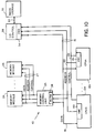
- FIG. 10 there is shown another embodiment of the system 10 that is constructed and operated in accordance with a presently preferred embodiment of the invention.
- those elements having reference numerals in common with Fig. 1 operate as described above in relation to the description of the system 10 of Fig. 1.
- the system of Fig. 10 includes a plurality (n) of substantially identically constructed CPUs designated CPU0 12A through CPUn 12n.
- the system 10 may include up to four of the CPUs 12 (CPU0-CPU3).
- Each of the CPUs 12A-12n executes an associated operating system (OS) program that, in the presently preferred embodiment of the invention, is known as the VS Operating System available from Wang Laboratories of Lowell, Massachusetts.
- OS operating system
- Each of the CPUs 12A-12n may be substantially identical to the CPU of Fig. 1. As such, each of the CPUs includes an associated VMC 14A-14n.
- the address bus 20 is comprised of 28 address lines and is coupled to each VMC 14, the state of the address bus 20 being expressive of a physical address within, for example, one of the memory modules 24 or 26.
- Each VMC 14A-14n translates a virtual memory address generated by the associated CPU 12A-12n into a physical memory address.
- the control bus 22 comprises memory and I/O read and write signal lines and other signal lines such as lines expressive of bus error conditions, bus arbitration states, bus access type and bus timing and synchronization.
- the data bus 18 is comprised, in this embodiment, of 64 data lines.
- Memory modules 24 and 26 are each coupled to the CPUs 12A-12n through the MCU 25 via the memory bus 27.
- MCU 25 performs memory timing, selection, control and refresh function; such as multiplexing the address bus 20 into memory row and column addresses and asserting row and column address strobe signals.
- the MCU 25 also performs arbitration to manage competing requests for access to the Memory Modules 24 and 26. Memory arbitration is accomplished with a prioritized round-robin technique.
- the MCU 25 further includes the RCTM 36.
- the RCTM 36 is coupled to certain of the system bus 16 signal lines in a manner to be described below.
- the RCTM 36 is located upon the MCU 25 and is responsive to accesses to any of the MMs 24-26 the RCTM contains status bits indicative of the reference and change activity of all of page frames of the system memory that is accessible by any of the CPUs 12A-12n.
- each of the CPUs 12A-12n has access to the page frames of the system memory each of the CPUs 12A-12n is further enabled, via VS privileged instructions, to test (read) and reset (clear) through the system bus 16 the memory page frame status bits that are generated and stored by the RCTM 36.
- the RCTM 36 provides to the multiple data processors, in a centralized and readily accessible location, status information relating to page frames of memory stored within the system memory.
- memory module 24 comprises a plurality of memory devices 40, which in an illustrative embodiment of the invention are each dynamic random access memory (DRAM).
- DRAM dynamic random access memory
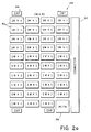
- the memory module 24 comprises 39 DRAM devices, each of which is operable for storing approximately one million bits of information.
- the remaining seven DRAM devices store error detection and correction bits which are utilized to detect double bit and correct single bit data errors which may occur within the DRAM devices 40.
- the memory module 24 may also comprise a connector 42 which is operable for coupling a plurality of digital signals from, for example, the bus 27 to the memory module 24. These signals include operating power (+5V and 0V), a plurality of multiplexed address lines (A0-A9), a plurality of data lines (D0-D31 or D0-D63), the error detection and correction data bits (CB0-CB6), and a plurality of memory control signal lines (RAS*, CAS*, W*).
- the memory module 24 also comprises the aforementioned RCTM 36, which is also coupled to certain of the signal lines (A0-A9, RAS*, CAS*, W*, RRCT*, TRCT*, I/O and UPPER) in a manner which will be disclosed below.
- the MCU 25 includes the RCTM 36 which is coupled to address signal lines and to the memory control and other signals (RAS*, CAS*, W*, RRCT*, TRCT*, I/O and UPPER) in a manner disclosed below.
- the memory module 24 also comprises a substrate, which may be a printed circuit card of well known construction having the plurality of memory devices soldered or otherwise coupled thereto, including the RCTM 36 and other components such as power supply filtering capacitors 44.
- RCTM 36 may be comprised of a plurality of discrete logic devices coupled together as will be described.
- RCTM 36 is a unitary integrated circuit device, such as a gate array, which achieves a lower power consumption and a lower surface area utilization than a plurality of devices.
- the modular RCTM of the invention is not limited to being employed upon discrete memory modules coupled to a system bus.
- a system bus it may be desirable to provide one unitary substrate having all of the system components physically mounted thereon.
- one or more memory units would be attached to the substrate along with a data processor, a system bus, VMC and other components.
- Each memory unit may then be associated with one of the modular RCTMs.
- the RCTMs would be coupled to the appropriate signal lines for recording the reference and change status of an associated memory unit, such as a four megabyte unit.
- the memory module shown in Fig. 2a is capable of storing in excess of four megabytes of data, or one megaword, each word being comprised of 32 bits of data. It can be appreciated that two such modules may be operated in parallel to store words having 64 bits of data, four modules may store words having 128 bits of data, etc.
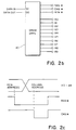
- a well known DRAM having a Data In and a Data Out signal line and a plurality of address lines A0 through A9.
- the DRAM 40 also has a RAS*, CAS*, and R/W* signal control line.
- DRAMs typically multiplex the address lines such that at one time in the operation of the device the address lines are characterized as row address lines under the control of RAS* and at another time in the cycle are characterized as column address lines under the control of CAS*.
- 2b has ten address signal pins and, thus, has a total of 20 address inputs which yield a device having a total of 1,048,567 bit storage locations.
- other DRAMs may have more or less than ten address inputs such as 64K and 256k bit devices and other devices may store more than one bit of data, such as devices adapted to simultaneously store and retrieve four bits of data.
- one conventional addressing mode for such a DRAM results in RAS* being asserted for latching within the RAM the row address lines appearing on A0-A9. Subsequent to the assertion of RAS* the state of the address lines A0-A9 are switched to the desired column address and CAS* is asserted. The assertion of CAS* also typically either stores within the device or reads from the device, depending upon the state of R/W*, a bit of data at the specified row and column address.
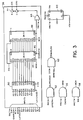
- RCTM 36 can be seen to comprise a first memory device 46 and a second memory device 48.
- Memory devices 46 and 48 each have, in this embodiment of the invention, a storage capacity of 2048 bits of data.
- the 2048 bit storage capacity of each of the memory devices 46 and 48 corresponds to 2048 blocks, or page frames, of physical memory; that is 2048 page frames each comprising 512 32 bit words of data.
- Memory device 46 is configured such that an access by CPU 12 to the memory devices 40 on the memory module 24 results in a corresponding bit being set to a logic one condition.
- Memory device 48 is configured such that a write access to a memory device upon the memory module also results in a corresponding bit being set to a logic one. Thus, it can be seen that memory device 46 records the occurrence of a reference to a particular page of data while memory device 48 further records the occurrence of a write, or change, of a particular page of data.
- memory devices 46 and 48 have 11 address inputs (A0-A10).
- A1-A10 are coupled to the output of a ten bit latch 50 which latches the state of the A0-A9 address bits from the address bus 20.
- This latching function may be accomplished by the falling edge of the memory row address strobe (RAS*).
- RAS* memory row address strobe
- the falling edge of RAS* occurs during the strobing of the row address into the memory devices 40 of Fig. 2a.
- RAS* is applied to a clock input of latch 50 via NAND gate 52.
- a second input to NAND gate 52 is a normally high signal UPPER*, the operation of which will be described hereinafter.
- the eleventh address input to memory devices 46 and 48 is subsequently applied after the falling edge of RAS*, being the A9 address signal, which is typically applied during the column address strobe (CAS*) portion of the memory 40 access cycle.
- RAS* the falling edge of RAS*
- CAS* column address strobe
- a presently preferred embodiment of a memory module described herein comprises, as illustrated in Fig. 6, 1,048,567 data words each comprising 32 bits of data, for a memory module storage capacity of more than four million bytes of data.
- the memory module may comprise more or less than this number of data storage locations.
- the memory devices 46 and 48 in these other, unillustrated, embodiments will correspondingly have fewer or more storage locations.
- a page frame of data is defined to be other than 512 data words, such as 256 or 1024 data words, the storage capacity of each of the memory devices 46 and 48 may also differ from that shown herein.
- the presently preferred embodiment of the invention is shown to utilize dynamic random access memory, such memories typically requiring the RAS* and CAS* timing signals.
- the memory devices 40 may be static type memory devices which do not require RAS* and CAS* timing signals.
- any type of memory device, such as bubble memory, may be utilized upon a memory module 24 or 26.
- the RCTM 36 is provided with sufficient address inputs and storage locations to record accesses to a number of memory page frames expressive of a maximum capacity of the common system memory, as is described below.
- a write input (W*) of memory device 46 is an AND gate 56 having as inputs the CAS* memory timing signal and a read reference and change table (RRCT*) signal, the operation of which will be described hereinafter.
- RRCT* read reference and change table
- the DI input of memory device 46 is coupled to the output of a flip/flop (FF) 60 which has a Read Reference and Change Table (RRCT*) signal coupled to a D input thereof and a clock signal coupled to the clock input.
- FF flip/flop
- RRCT* Read Reference and Change Table
- RRCT* is a logic one; making DIN normally a logic one.
- a logic one is stored within the memory device 46 at a location corresponding to the page frame addressed by CPU 12. The storage of such a logic one signal is indicative of a reference to a particular page frame by the CPU 12.
- Memory device 48 is similarly coupled to the address signals and the output of FF 60 and, further, has an AND gate 58 coupled to the W* thereof, the AND gate 58 having as inputs the memory write (W*) timing signal and the RRCT* timing signal.
- the state of the W* timing signal is indicative of a CPU 12 write access to the memories 40 of memory module 24.
- the assertion of W* stores a logic one in the memory location addressed by address inputs A0-A10 of memory device 48. This is indicative of a change to the corresponding page frame of physical memory.
- the W* signal line is not asserted. Thus, only the corresponding bit in memory device 46 is set. Only during a CPU 12 write access to a particular page of physical memory are both the reference and change bits set in devices 46 and 48, respectively.
- Memory devices 46 and 48 each have a chip select input (CS*) which is normally required to be at a logic low state in order to read or write data within the memory device.
- the CS* signals of memory devices 46 and 48 are coupled, via NAND gate 62, to an active low signal I/O ⁇ , which is normally at a logic zero state and to an active high bank select (BANK SEL) signal.
- I/O* active low signal
- BANK SEL active high bank select
- the BANK SEL input to NAND gate 62 is high when the bank of memory associated with RCT 36 is selected.
- the combination of I/O* being deasserted, or high, and BANK SEL being asserted drives the output of NAND gate 62 low, thereby selecting both memory devices 46 and 48.
- a 32 bit local address bus has, for a 32 bit data bus embodiment, ten MSB bits as bank select addresses.
- a 64 bit data bus system has nine MSB address bus bits as bank select addresses. It can be appreciated that a 32 data bit system comprises four bytes of data per word while a 64 data bit system comprises eight bytes of data per word. Byte selection is accomplished by decoding either two or three LSB address bits. Such bank and byte select decoding is typically accomplished by address decoding means within the MCU 25.
- the I/O* signal is provided to prevent the operation of memory devices 46 and 48 during an I/O type of memory 40 access, such as when the I/O controller 28 is storing or retrieving data within the memories 40.
- the information stored within memory devices 46 and 48 must be operable for at least being read and possibly modified by a physical memory controlling device, such as a software routine executed by the CPU 12 which manages the physical memory. For example, it may be desirable after a predetermined interval of time to examine the memory device 46 to determine which pages of memory have been accessed by CPU 12 and which pages have not been accessed. If, after a given interval of time, one or more pages of data have not been accessed by CPU 12 the continued residency of these pages of data within the physical memory may be unnecessary. Thus, it may be desirable in some situations to remove an unreferenced page of data from memory and to store in its place another page of data, such as a page of memory which is currently being requested by the CPU 12.
- This aspect of the invention is especially advantageous in the embodiment of Fig. 10 wherein a plurality of the CPUs 12 each have access over the system bus 16 to the RCTM 36 information.
- the RCTM 36 is operable for having individual bits of the memory devices 46 and 48 selectively reset to a logic zero condition. This is accomplished by asserting the reset reference and change table (RRCT*) signal in conjunction with the desired address of the page within the memory devices 46 and 48. As can be seen in Fig. 3 and 4b, when RRCT* is low, or asserted, the data input (DIN) to each of the memory devices 46 and 48 is at a logic zero condition via F/F 60. The assertion of RRCT*, being coupled through AND gates 56 and 58 to the write inputs of memory devices 46 and 48, respectively, causes a logic zero to be written into the addressed memory location.
- RRCT* reset reference and change table
- the address inputs A0-A9 are first set up as previously described, the address bits being latched into latch 50 by the assertion of signal UPPER*.
- the resetting of bits within memory devices 46 and 48 is accomplished, for example, when a new block of data is stored within the physical memory.
- the RCTM 36 is provided with a test reference and change table (TRCT*) signal.
- TRCT* test reference and change table
- the TRCT* signal is provided, via OR gate 66, to an output enable (OE*) input of buffer 64 to cause the buffer 64 to place the logic states of R and C on a pair of outputs coupled to the most significant bit (MSB) and the second most significant bit (MSB-1) of the data bus.
- the CPU 12 is enabled to read the addressed location within memory devices 46 and 48 to determine the reference and change status of the corresponding page of physical memory.
- these accesses to RCTM 36 as defined by TRCT* and RRCT* are not memory-type accesses to prevent the storage of reference and change bits within memory devices 46 and 48.
- RRCT* and TRCT* are asserted by the execution of operating system privileged instructions, that is, instructions that cannot be executed by a user's program.
- these privileged instructions are instructions that operate in the I/O address space.
- the reference and change table is not centralized nor need it be physically adjacent the CPU 12 or the VMC 14. Instead, the RCT is distributed throughout the physical memory space of the data processing system 10.
- additional memory modules may be attached to the system, each of the memory modules having an internal, modular RCTM for recording the reference and change activity upon that particular memory module.
- the data processing system may have its physical memory capacity expanded without exceeding the storage capability of any one particular RCTM.
- the virtual memory data processing system 10 is not burdened with excess cost and complexity by having a unitary reference and change table which has a predetermined storage capacity which far exceeds the actual physical memory storage capacity of the system.
- the virtual memory data processing system 10 is provided with a flexible and expandable reference and change table which is expanded as physical memory capacity is attached to the system, thereby providing for a reduction in system cost and the readily accomplished memory expansion of the system.
- a readily accomplished memory expansion is especially advantageous for those systems which have their physical memory capacity increased at a time subsequent to the initial installation of the system.
- the system reference and change table is automatically expanded during the installation of one or more additional memory modules.
- the RCTM 36 is located upon the MCU 25.
- the RCTM 36 is located upon the MCU 25 and is responsive to accesses made to any of the MMs 24-26 the RCTM 36 contains status bits indicative of the reference and change activity of all of page frames of the system memory that are accessed by any of the CPUs 12A-12n.
- each of the CPUs 12A-12n has access to the page frames of the system memory each of the CPUs 12A-12n is further enabled, via the VS-privileged instructions, to test (read) and reset (clear) over the system bus 16 the memory page frame status bits that are generated and stored by the RCTM 36.
- the RCTM of the presently preferred embodiment of the invention provides to multiple data processors a centralized and readily accessible store of status information relating to page frames of memory stored within the system memory.
- the RCTM 36 may be provided as two devices, each containing 128Kbits of storage organized as two 64K X 1 memory devices. As such, each RCTM 36 device is capable of storing reference and change bits for 128 MBytes of physical memory organized as 2Kbyte page frames. In a presently preferred embodiment of the invention the RCTM 36 is provided as four 64K X 1 memory devices, two for storing change bits and two for storing reference bits.
- the MCU 25 arbitrates accesses to the RCTM 36 by the CPUs 12A-12n in a manner similar to that employed to manage accesses to the physical memory.
- the MCU 25 detects a request for access, arbitrates the request employing the prioritized round-robin technique, decodes memory access control lines 22 from the bus 16 into an access type, asserts the applicable TRCT* or RRCT* signal ine, and performs the access to the specified RCTM 36 device.
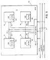
- a memory carrier module (MCM) 70 which, in accordance with the invention, comprises a substrate, such as a printed circuit board, having a plurality of memory modules (MM) 72-78 disposed upon a surface 71 thereof.
- MCM memory carrier module
- Each of the MMs 72-78 may be identical in construction to the memory module 24 of Fig. 2a, that is, each of the MMs 72-78 comprises an integral reference and change table module (RCTM) 80-86, respectively.
- Each of the RCTMs 80-86 may be identical in construction to the RCTM 36 of Fig. 3. It should be realized that more or less than the four MMs shown may be provided on the MCM and that less than the possible maximum number may be installed at any given time.
- MCM 70 may comprise logic means, such as a memory carrier module control (MCM CONTROL) 88, which is operable for interfacing with the memory bus 27.
- MCM CONTROL 88 decodes the address and control buses to select a particular MM 72-78 for read or write access by the CPU 12 or I/O control 28.
- MCM CONTROL 88 may also be operable for generating the multiplexed row and column address signals on A0-A9, the RAS* and CAS* signals, and the logic signals associated with the RCTMs 80-86, such as RRCT*, TRCT* and UPPER.
- MCM CONTROL 88 may comprise a well-known DRAM controller type of device and other circuits, such as address decoders, and row and column address multiplexers. Of course, these MCM control functions may also be accomplished by the MCU 25 of Fig. 1, either operating alone or in conjunction with MCM control 88.
- MCM CONTROL 88 may have a number of CAS* outputs equal to the numbers of MMs installed, only one of the CAS* outputs being asserted for any given CPU 12 or I/O access.
- the MCM CONTROL 88 may have a plurality of RRCT* and TRCT* outputs for individually activating the RCTMs 80-86.
- MCM CONTROL 88 may be operable for generating a common MM signal group 90 which includes those logic signals, such as A0-A9, UPPER, and RAS* which are provided in common to each of the MMs. MCM CONTROL 88 may further be operable for generating a plurality of MM specific signal groups 92-96, coupled to MMs 72-76, respectively. Each specific signal group is comprised of signals operable for activating only a selected MM, such as CAS*, W*, RRCT*, I/O and TRCT*.
- the total storage capacity of the MCM 70 may vary from four megabytes to 16 megabytes of data, depending on the number of MMs installed.
- the total RCTM storage capacity therefore is similarly variable between 2048 and 8192 two bit words of data, corresponding to the total number of physical page frames represented by the installed memory capacity of MCM 70.
- Each memory module 72-78 may be comprised of 16 memory devices and a corresponding fewer number of error detection and correction memory devices coupled to a 16 bit data bus. In some systems however it may be desirable to employ an expanded data path, such as a data path comprised of 64 or 128 bits.
- a 64 bit system is illustrated in Fig. 8.
- Logic operable for generating certain of the RCTM input signal is shown schematically in Fig. 9.
- the data bus may comprise data signal lines D00-D63 coupled to the MCM 70.
- the 32 bit MMs 72 and 74 may then each store one half of the 64 bit data word.
- the lower 32 bits may be stored in MM 72 and the upper 32 bits in MM 74.
- MCM CONTROL 88 may comprise additional circuitry for bank selecting either or both of the MMs 72 and 74 depending upon the type of CPU access.
- a long word (64 bit) access would result in the selection of both MM 72 and 74 while a word access (32 bits) would select only one of the MMs 72 or 74.
- the bank selection would not only enable the memory devices upon the selected MM but would also enable the associated RCTM.
- the decoded higher order address signal line modifies the state of an MM specific signal, such as ENABLE*.
- the I/O ⁇ signal line may be combined with a BANK SEL signal as illustrated in Fig. 3.
- the modular RCTM of the invention may be readily employed in a number of different types of data processing systems having varying data word widths and/or depth.
- RCTM is shown to comprise two separate memory devices 46 and 48, it is within the scope of the invention to provide one memory device having a storage capacity of two or more bits per address location.
- the invention is not to be limited to this presently preferred embodiment but is instead to be limited only as defined by the appended claims.
Abstract
Claims (9)
- Système informatique à mémoire virtuelle (10) comprenant :- des moyens de traitement de données reliés à un bus de système (16) et émettant des adresses de mémoire physique vers le bus de système (16),- des moyens de mémoire physique organisés en n unités adressables (24, ..., 26), dont chacune comprend une pluralité d'emplacements d'adresses de mémoire physique,- un contrôleur d'accès à la mémoire (25) comprenant :- une interface de bus de système pour coupler ledit contrôleur d'accès à la mémoire (25) auxdits moyens de traitement de données par l'intermédiaire dudit bus de système (16), et- une interface de moyens de mémoire qui comprend une pluralité de lignes de transfert de signaux de moyens de mémoire (27) pour coupler ledit contrôleur d'accès à la mémoire (25) auxdits moyens de mémoire physique, et- des moyens de stockage de table de référence et de modification (36) comprenant :caractérisé en ce que :- des premiers moyens pour enregistrer une apparition d'un accès à un emplacement d'adresse spécifique à l'intérieur des moyens de mémoire physique par les moyens de traitement de données,- des seconds moyens pour enregistrer un type d'accès à l'emplacement d'adresse spécifique,- des troisièmes moyens, réagissant à un premier type d'accès par les moyens de traitement de données, pour émettre un contenu d'un emplacement spécifié à l'intérieur des premiers moyens d'enregistrement et des seconds moyens d'enregistrement, et- des quatrième moyens, réagissant à un second type d'accès par les moyens de traitement de données, pour remettre à zéro un emplacement spécifié dans les premiers moyens d'enregistrement et les seconds moyens d'enregistrement pour indiquer, pour l'unité adressable correspondante (24, ..., 26), une condition d'absence d'accès,- lesdits moyens de traitement de données comprennent une pluralité de processeurs (12a, ..., 12n),- ledit système informatique à mémoire virtuelle (10) comprend un seul desdits moyens de stockage de table de référence et de modification (36),- ledit seul moyen de stockage de table de référence et de modification (36) est :- physiquement et électriquement couplé audit contrôleur d'accès à la mémoire (25) pour enregistrer des accès auxdits moyens de mémoire physique par chacun de ladite pluralité de processeurs (12a, ..., 12n), est- accessible à son tour à certains processeurs individuels de ladite pluralité de processeurs (12a, ..., 12n) sous la direction dudit contrôleur d'accès à la mémoire (25), et est- sensible aux adresses de mémoire physiques reçues par ledit bus de système (16) et provenant de l'un quelconque de la pluralité de processeurs (12a, ..., 12n) pour enregistrer l'apparition de, et le type de l'accès effectué à l'une quelconque desdites n unités adressables (24, ..., 26), et- ledit contrôleur d'accès à la mémoire (25) comprend des moyens pour arbitrer des accès auxdits moyens de stockage de table de référence et de modification (36) par des processeurs individuels de ladite pluralité de processeurs (12a, ..., 12n) lorsque lesdits processeurs individuels de ladite pluralité de processeurs (12a, ..., 12n) effectuent l'un desdits premier et second types d'accès auxdits moyens de stockage de table de référence et de modification (36).
- Système informatique (10) selon la revendication 1 dans lequel :- ledit système informatique (10) comprend de plus des moyens d'E/S qui sont couplés auxdits moyens de mémoire physique par ledit bus de système (16), lesdits moyens d'E/S servant à accéder par ledit bus de système (16) à un emplacement d'adresse spécifique à l'intérieur desdits moyens de mémoire, et- lesdits moyens de stockage de table de référence et de modification (36) comprennent des moyens, réagissant à un accès mémoire par lesdits moyens d'E/S, pour invalider une opération desdits moyens de stockage de table de référence et de modification (36).
- Système informatique (10) selon la revendication 1 dans lequel- chacun desdits processeurs (12a, ..., 12n) comprend des moyens de contrôleur de mémoire virtuelle (14a, ..., 14n) pour générer une adresse physique en réponse à une adresse de mémoire virtuelle, chacun desdits moyens de contrôleur de mémoire virtuelle (14a, ..., 14n) ayant une sortie couplée au bus de système (16) pour lui appliquer l'adresse physique.
- Système informatique (10) selon la revendication 1 dans lequel- lesdits premiers moyens d'enregistrement et seconds moyens d'enregistrement comprennent chacun un nombre prédéterminé d'emplacements de mémoire au moins égal au nombre prédéterminé d'unités adressables (24, ..., 26),- lesdits moyens de stockage de table de référence et de modification (36) comprenant de plus :- des moyens, réagissant à une adresse physique appliquée audit bus de système (16), pour stocker des données à un emplacement de mémoire à l'intérieur desdits premiers moyens d'enregistrement et desdits seconds moyens d'enregistrement qui correspond à un numéro de l'une des unités adressables (24, ..., 26), les données stockées étant représentatives de l'apparition d'un accès à et d'un type d'accès à l'unité adressable (24, ..., 26),- des moyens, réagissant à une adresse appliquée audit bus de système (16), pour extraire des données stockées desdits premiers moyens d'enregistrement et desdits seconds moyens d'enregistrement et les transmettre audit bus de système (16) à partir d'un emplacement de mémoire correspondant à l'une des unités adressables.
- Système informatique (10) selon la revendication 1 dans lequel ledit bus de système (16) comprend :- une pluralité de lignes de transfert de signaux d'adresses (20);- une pluralité de lignes de transfert de signaux de commande (22); et- une pluralité de lignes de transfert de données (18) ayant un bit de poids fable (LSB) et un bit de poids fort (MSB); et dans lequel- certaines de ladite pluralité de lignes de transfert de signaux de commande (22) transfèrent une information représentative d'une commande d'émettre un signal de remise à zéro de table de référence et de modification, l'émission dudit signal de remise à zéro de table de référence et de modification remettant à zéro l'un choisi desdits emplacements de stockage de moyens de table de référence et de modification pour indiquer une condition d'absence d'accès, en réalisant ainsi ledit second type d'accès.
- Système informatique (10) selon la revendication 5 dans lequel- lesdites certaines de ladite pluralité de lignes de transfert de signaux de commande (22) transfèrent de plus une information représentative d'une commande d'émettre un signal de test de table de référence et de modification, l'émission dudit signal de test de table de référence et de modification activant lesdits moyens de table de référence et de modification (36) pour leur faire émettre les contenus de l'un choisi desdits emplacements de mémoire en réalisant ainsi ledit premier type d'accès.
- Système informatique (10) selon la revendication 6 dans lequel lesdits moyens de stockage de table de référence et de modification (36) comprennent :- des moyens, réagissant à l'émission dudit signal de test de table de référence et de modification, pour coupler une première et une seconde ligne de transfert de signaux de sortie de moyens de table de référence et de modification à des lignes prédéterminées parmi les lignes de transfert de données du bus de système (18).
- Système informatique (10) selon la revendication 7 dans lequel- lesdites lignes prédéterminées parmi lesdites lignes de transfert de données du bus de système (18) sont la MSB et une (MSB-1).
- Moyens de stockage de table de référence et de modification (36) d'un système informatique (10) selon l'une quelconque des revendications 1 à 8.
Applications Claiming Priority (3)
| Application Number | Priority Date | Filing Date | Title |
|---|---|---|---|
| US07/463,640 US5155834A (en) | 1988-03-18 | 1990-01-11 | Reference and change table storage system for virtual memory data processing system having a plurality of processors accessing common memory |
| US463640 | 1990-01-11 | ||
| PCT/US1990/004176 WO1991010956A1 (fr) | 1990-01-11 | 1990-07-25 | Table centralisee de modification et de barême pour systeme de memoire virtuelle d'un multicalculateur |
Publications (2)
| Publication Number | Publication Date |
|---|---|
| EP0509994A1 EP0509994A1 (fr) | 1992-10-28 |
| EP0509994B1 true EP0509994B1 (fr) | 1997-01-22 |
Family
ID=23840810
Family Applications (1)
| Application Number | Title | Priority Date | Filing Date |
|---|---|---|---|
| EP90911530A Expired - Lifetime EP0509994B1 (fr) | 1990-01-11 | 1990-07-25 | Table centralisee de modification et de reference pour systeme de memoire virtuelle d'un multicalculateur |
Country Status (7)
| Country | Link |
|---|---|
| US (1) | US5155834A (fr) |
| EP (1) | EP0509994B1 (fr) |
| JP (1) | JPH05503382A (fr) |
| AU (1) | AU648259B2 (fr) |
| CA (1) | CA2073677C (fr) |
| DE (1) | DE69029815T2 (fr) |
| WO (1) | WO1991010956A1 (fr) |
Families Citing this family (16)
| Publication number | Priority date | Publication date | Assignee | Title |
|---|---|---|---|---|
| US5339397A (en) * | 1990-10-12 | 1994-08-16 | International Business Machines Corporation | Hardware primary directory lock |
| US5247642A (en) * | 1990-12-05 | 1993-09-21 | Ast Research, Inc. | Apparatus for determining cacheability of a memory address to provide zero wait state operation in a computer system |
| JP3259969B2 (ja) * | 1991-07-09 | 2002-02-25 | 株式会社東芝 | キャッシュメモリ制御装置 |
| US5414821A (en) * | 1991-12-17 | 1995-05-09 | Unisys Corporation | Method of and apparatus for rapidly loading addressing environment by checking and loading multiple registers using a specialized instruction |
| JP3437852B2 (ja) * | 1992-10-07 | 2003-08-18 | 富士通株式会社 | ページング機能を持つデータ処理装置 |
| JP3604176B2 (ja) * | 1994-09-14 | 2004-12-22 | 株式会社東芝 | 仮想空間管理方法及び分散処理システム |
| US5761740A (en) * | 1995-11-30 | 1998-06-02 | Unisys Corporation | Method of and apparatus for rapidly loading addressing registers |
| US6493347B2 (en) | 1996-12-16 | 2002-12-10 | Juniper Networks, Inc. | Memory organization in a switching device |
| US5956754A (en) * | 1997-03-03 | 1999-09-21 | Data General Corporation | Dynamic shared user-mode mapping of shared memory |
| US6026466A (en) * | 1997-06-16 | 2000-02-15 | Integrated Silicon Solution, Inc. | Multiple row address strobe DRAM architecture to improve bandwidth |
| US6108761A (en) * | 1998-02-20 | 2000-08-22 | Unisys Corporation | Method of and apparatus for saving time performing certain transfer instructions |
| US6081881A (en) * | 1998-02-20 | 2000-06-27 | Unisys Corporation | Method of and apparatus for speeding up the execution of normal extended mode transfer instructions |
| US6892263B1 (en) * | 2000-10-05 | 2005-05-10 | Sun Microsystems, Inc. | System and method for hot swapping daughtercards in high availability computer systems |
| US6622229B2 (en) | 2001-02-28 | 2003-09-16 | International Business Machines Corporation | Virtual memory structure |
| US20100325327A1 (en) * | 2009-06-17 | 2010-12-23 | Freescale Semiconductor, Inc. | Programmable arbitration device and method therefor |
| US20100325519A1 (en) * | 2009-06-17 | 2010-12-23 | Microsoft Corporation | CRC For Error Correction |
Citations (1)
| Publication number | Priority date | Publication date | Assignee | Title |
|---|---|---|---|---|
| EP0333215A2 (fr) * | 1988-03-18 | 1989-09-20 | Wang Laboratories Inc. | Table distribuée de référence et de changement pour un système de mémoire virtuelle |
Family Cites Families (27)
| Publication number | Priority date | Publication date | Assignee | Title |
|---|---|---|---|---|
| GB1461245A (en) * | 1973-01-28 | 1977-01-13 | Hawker Siddeley Dynamics Ltd | Reliability of random access memory systems |
| US3840863A (en) * | 1973-10-23 | 1974-10-08 | Ibm | Dynamic storage hierarchy system |
| US4055851A (en) * | 1976-02-13 | 1977-10-25 | Digital Equipment Corporation | Memory module with means for generating a control signal that inhibits a subsequent overlapped memory cycle during a reading operation portion of a reading memory cycle |
| US4042911A (en) * | 1976-04-30 | 1977-08-16 | International Business Machines Corporation | Outer and asynchronous storage extension system |
| US4096568A (en) * | 1976-09-24 | 1978-06-20 | Sperry Rand Corporation | Virtual address translator |
| US4181937A (en) * | 1976-11-10 | 1980-01-01 | Fujitsu Limited | Data processing system having an intermediate buffer memory |
| US4084230A (en) * | 1976-11-29 | 1978-04-11 | International Business Machines Corporation | Hybrid semiconductor memory with on-chip associative page addressing, page replacement and control |
| US4128875A (en) * | 1976-12-16 | 1978-12-05 | Sperry Rand Corporation | Optional virtual memory system |
| US4126894A (en) * | 1977-02-17 | 1978-11-21 | Xerox Corporation | Memory overlay linking system |
| US4277826A (en) * | 1978-10-23 | 1981-07-07 | Collins Robert W | Synchronizing mechanism for page replacement control |
| US4290104A (en) * | 1979-01-02 | 1981-09-15 | Honeywell Information Systems Inc. | Computer system having a paging apparatus for mapping virtual addresses to real addresses for a memory of a multiline communications controller |
| US4340776A (en) * | 1980-10-29 | 1982-07-20 | Siemens Corporation | Modular telecommunication system |
| US4414624A (en) * | 1980-11-19 | 1983-11-08 | The United States Of America As Represented By The Secretary Of The Navy | Multiple-microcomputer processing |
| US4410941A (en) * | 1980-12-29 | 1983-10-18 | Wang Laboratories, Inc. | Computer having an indexed local ram to store previously translated virtual addresses |
| US4445170A (en) * | 1981-03-19 | 1984-04-24 | Zilog, Inc. | Computer segmented memory management technique wherein two expandable memory portions are contained within a single segment |
| DE3276916D1 (en) * | 1981-09-18 | 1987-09-10 | Rovsing As Christian | Multiprocessor computer system |
| US4608631A (en) * | 1982-09-03 | 1986-08-26 | Sequoia Systems, Inc. | Modular computer system |
| US4484273A (en) * | 1982-09-03 | 1984-11-20 | Sequoia Systems, Inc. | Modular computer system |
| DE3382152D1 (de) * | 1982-12-09 | 1991-03-07 | Sequoia Systems Inc | Sicherstellungsspeichersystem. |
| USRE37305E1 (en) * | 1982-12-30 | 2001-07-31 | International Business Machines Corporation | Virtual memory address translation mechanism with controlled data persistence |
| US4714993A (en) * | 1983-10-18 | 1987-12-22 | International Business Machines Corporation | Apparatus and method for effecting dynamic address translation in a microprocessor implemented data processing system |
| US4680700A (en) * | 1983-12-07 | 1987-07-14 | International Business Machines Corporation | Virtual memory address translation mechanism with combined hash address table and inverted page table |
| US4792895A (en) * | 1984-07-30 | 1988-12-20 | International Business Machines Corp. | Instruction processing in higher level virtual machines by a real machine |
| US4758993A (en) * | 1984-11-19 | 1988-07-19 | Fujitsu Limited | Random access memory device formed on a semiconductor substrate having an array of memory cells divided into sub-arrays |
| JPS61214298A (ja) * | 1985-03-20 | 1986-09-24 | Toshiba Corp | 誤り訂正機能を備えた半導体記憶装置 |
| JPH0814803B2 (ja) * | 1986-05-23 | 1996-02-14 | 株式会社日立製作所 | アドレス変換方式 |
| US4807189A (en) * | 1987-08-05 | 1989-02-21 | Texas Instruments Incorporated | Read/write memory having a multiple column select mode |
-
1990
- 1990-01-11 US US07/463,640 patent/US5155834A/en not_active Expired - Lifetime
- 1990-07-25 EP EP90911530A patent/EP0509994B1/fr not_active Expired - Lifetime
- 1990-07-25 CA CA002073677A patent/CA2073677C/fr not_active Expired - Lifetime
- 1990-07-25 JP JP2511103A patent/JPH05503382A/ja active Pending
- 1990-07-25 WO PCT/US1990/004176 patent/WO1991010956A1/fr active IP Right Grant
- 1990-07-25 AU AU60794/90A patent/AU648259B2/en not_active Expired
- 1990-07-25 DE DE69029815T patent/DE69029815T2/de not_active Expired - Lifetime
Patent Citations (1)
| Publication number | Priority date | Publication date | Assignee | Title |
|---|---|---|---|---|
| EP0333215A2 (fr) * | 1988-03-18 | 1989-09-20 | Wang Laboratories Inc. | Table distribuée de référence et de changement pour un système de mémoire virtuelle |
Also Published As
| Publication number | Publication date |
|---|---|
| JPH05503382A (ja) | 1993-06-03 |
| DE69029815T2 (de) | 1997-07-31 |
| CA2073677A1 (fr) | 1991-07-12 |
| CA2073677C (fr) | 2000-03-14 |
| EP0509994A1 (fr) | 1992-10-28 |
| US5155834A (en) | 1992-10-13 |
| AU648259B2 (en) | 1994-04-21 |
| DE69029815D1 (de) | 1997-03-06 |
| WO1991010956A1 (fr) | 1991-07-25 |
| AU6079490A (en) | 1991-08-05 |
Similar Documents
| Publication | Publication Date | Title |
|---|---|---|
| US5155833A (en) | Multi-purpose cache memory selectively addressable either as a boot memory or as a cache memory | |
| EP0509994B1 (fr) | Table centralisee de modification et de reference pour systeme de memoire virtuelle d'un multicalculateur | |
| EP0090575B1 (fr) | Système de mémoire | |
| US5265231A (en) | Refresh control arrangement and a method for refreshing a plurality of random access memory banks in a memory system | |
| US5761695A (en) | Cache memory control method and apparatus, and method and apparatus for controlling memory capable of interleave control | |
| US5341494A (en) | Memory accessing system with an interface and memory selection unit utilizing write protect and strobe signals | |
| AU610226B2 (en) | Computer bus having page mode memory access | |
| US4513369A (en) | Information processing system | |
| US11669274B2 (en) | Write bank group mask during arbitration | |
| US11748034B2 (en) | Signalling for heterogeneous memory systems | |
| US4916603A (en) | Distributed reference and change table for a virtual memory system | |
| US5293622A (en) | Computer system with input/output cache | |
| EP0333215B1 (fr) | Table distribuée de référence et de changement pour un système de mémoire virtuelle | |
| EP0426386A2 (fr) | Dispositif de destination de données | |
| US5249277A (en) | Optimized performance memory method and system | |
| US11756606B2 (en) | Method and apparatus for recovering regular access performance in fine-grained DRAM | |
| JPH0450625B2 (fr) | ||
| JPS63266572A (ja) | デ−タ処理システム | |
| JPH03198288A (ja) | メモリアクセス制御装置 | |
| WO1992005491A1 (fr) | Procede et appareil pour selectionner la taille de la memoire |
Legal Events
| Date | Code | Title | Description |
|---|---|---|---|
| PUAI | Public reference made under article 153(3) epc to a published international application that has entered the european phase |
Free format text: ORIGINAL CODE: 0009012 |
|
| 17P | Request for examination filed |
Effective date: 19920709 |
|
| AK | Designated contracting states |
Kind code of ref document: A1 Designated state(s): BE DE FR GB NL |
|
| 17Q | First examination report despatched |
Effective date: 19930709 |
|
| GRAG | Despatch of communication of intention to grant |
Free format text: ORIGINAL CODE: EPIDOS AGRA |
|
| GRAH | Despatch of communication of intention to grant a patent |
Free format text: ORIGINAL CODE: EPIDOS IGRA |
|
| GRAH | Despatch of communication of intention to grant a patent |
Free format text: ORIGINAL CODE: EPIDOS IGRA |
|
| GRAA | (expected) grant |
Free format text: ORIGINAL CODE: 0009210 |
|
| AK | Designated contracting states |
Kind code of ref document: B1 Designated state(s): BE DE FR GB NL |
|
| PG25 | Lapsed in a contracting state [announced via postgrant information from national office to epo] |
Ref country code: NL Free format text: LAPSE BECAUSE OF FAILURE TO SUBMIT A TRANSLATION OF THE DESCRIPTION OR TO PAY THE FEE WITHIN THE PRESCRIBED TIME-LIMIT Effective date: 19970122 Ref country code: BE Effective date: 19970122 |
|
| REF | Corresponds to: |
Ref document number: 69029815 Country of ref document: DE Date of ref document: 19970306 |
|
| ET | Fr: translation filed | ||
| NLV1 | Nl: lapsed or annulled due to failure to fulfill the requirements of art. 29p and 29m of the patents act | ||
| PLBE | No opposition filed within time limit |
Free format text: ORIGINAL CODE: 0009261 |
|
| STAA | Information on the status of an ep patent application or granted ep patent |
Free format text: STATUS: NO OPPOSITION FILED WITHIN TIME LIMIT |
|
| 26N | No opposition filed | ||
| REG | Reference to a national code |
Ref country code: GB Ref legal event code: IF02 |
|
| REG | Reference to a national code |
Ref country code: GB Ref legal event code: 732E |
|
| REG | Reference to a national code |
Ref country code: FR Ref legal event code: TP |
|
| PGFP | Annual fee paid to national office [announced via postgrant information from national office to epo] |
Ref country code: FR Payment date: 20090710 Year of fee payment: 20 |
|
| PGFP | Annual fee paid to national office [announced via postgrant information from national office to epo] |
Ref country code: GB Payment date: 20090722 Year of fee payment: 20 Ref country code: DE Payment date: 20090723 Year of fee payment: 20 |
|
| REG | Reference to a national code |
Ref country code: GB Ref legal event code: PE20 Expiry date: 20100724 |
|
| PG25 | Lapsed in a contracting state [announced via postgrant information from national office to epo] |
Ref country code: GB Free format text: LAPSE BECAUSE OF EXPIRATION OF PROTECTION Effective date: 20100724 |
|
| PG25 | Lapsed in a contracting state [announced via postgrant information from national office to epo] |
Ref country code: DE Free format text: LAPSE BECAUSE OF EXPIRATION OF PROTECTION Effective date: 20100725 |