EP0507535B1 - Ein System zur Bestimmung des Funktionierens einer integrierten Schaltung - Google Patents
Ein System zur Bestimmung des Funktionierens einer integrierten Schaltung Download PDFInfo
- Publication number
- EP0507535B1 EP0507535B1 EP92302794A EP92302794A EP0507535B1 EP 0507535 B1 EP0507535 B1 EP 0507535B1 EP 92302794 A EP92302794 A EP 92302794A EP 92302794 A EP92302794 A EP 92302794A EP 0507535 B1 EP0507535 B1 EP 0507535B1
- Authority
- EP
- European Patent Office
- Prior art keywords
- alien
- entries
- model
- stimulus
- truth table
- Prior art date
- Legal status (The legal status is an assumption and is not a legal conclusion. Google has not performed a legal analysis and makes no representation as to the accuracy of the status listed.)
- Expired - Lifetime
Links
Images
Classifications
-
- G—PHYSICS
- G01—MEASURING; TESTING
- G01R—MEASURING ELECTRIC VARIABLES; MEASURING MAGNETIC VARIABLES
- G01R31/00—Arrangements for testing electric properties; Arrangements for locating electric faults; Arrangements for electrical testing characterised by what is being tested not provided for elsewhere
- G01R31/28—Testing of electronic circuits, e.g. by signal tracer
- G01R31/317—Testing of digital circuits
- G01R31/3181—Functional testing
- G01R31/3183—Generation of test inputs, e.g. test vectors, patterns or sequences
- G01R31/318342—Generation of test inputs, e.g. test vectors, patterns or sequences by preliminary fault modelling, e.g. analysis, simulation
- G01R31/318357—Simulation
-
- G—PHYSICS
- G06—COMPUTING OR CALCULATING; COUNTING
- G06F—ELECTRIC DIGITAL DATA PROCESSING
- G06F11/00—Error detection; Error correction; Monitoring
- G06F11/22—Detection or location of defective computer hardware by testing during standby operation or during idle time, e.g. start-up testing
- G06F11/26—Functional testing
- G06F11/261—Functional testing by simulating additional hardware, e.g. fault simulation
-
- G—PHYSICS
- G06—COMPUTING OR CALCULATING; COUNTING
- G06F—ELECTRIC DIGITAL DATA PROCESSING
- G06F30/00—Computer-aided design [CAD]
- G06F30/30—Circuit design
- G06F30/32—Circuit design at the digital level
- G06F30/33—Design verification, e.g. functional simulation or model checking
Definitions
- the present invention relates to a system for determining the operations of an integrated circuit and in particular a system for determining the operations of a custom chip.
- ASICs application specific integrated circuits
- custom chips often are not accompanied by documented information concerning their operations and functions.
- the minimum amount of information is usually only given such as the pin names, pin types (i.e. inputs, outputs etc.), pin ordering and so on.
- pin names i.e. inputs, outputs etc.
- pin ordering i.e. pin ordering
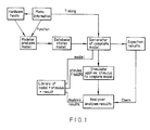
- a known system for obtaining such functions using a known computer and memories is shown schematically in figure 1.
- the testing system may be either a digital simulator, or an analogue simulator.
- a digital simulator is one that is event driven such that when a stimulus, is applied, the simulator notes that it should schedule an output change after a given period of time T. At T the next stimulus is then applied.
- An analogue simulator is not event driven. It applies a stimulus to an input pin and measures the voltage or current at an number of nodes in the ASIC model at equal intervals over a given time period. When testing the model using an analogue simulator it can take up to 10 to 20 hours to apply a particular type of stimulus to the model. If the ASIC is complex, any one of up to 9 types of stimulus may be required. Consequently, an analogue simulator is relatively slow, produces a far greater quantity of results but is more accurate than a digital simulator.
- the model is written in a particular computer language for use on a particular system. If the model is required on a non-complimentary system, then the modeler must rewrite the model in a suitable computer language. Consequently, ASIC foundaries often produce and support different systems containing the same libraries on the same ASIC. This is extremely time consuming and inefficient.
- An aim of the present invention is to provide a system which overcomes these disadvantages.
- a system for determining the operations of an integrated circuit comprising:
- the present invention thus provides a system using a known computer in conjunction with another computer housing an existing alien model (i.e. one that has already been generated by a modeler but in another language) and automatically generates a reference library from which other alien simulator libraries can be produced by extracting information from the reference library.
- an existing alien model i.e. one that has already been generated by a modeler but in another language
- the system is thus more efficient and quicker because only one model need be generated and the other simulators can be generated from the reference library.
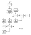
- a first embodiment of the present invention is shown in figure 2.
- the system comprises a translator 2 which receives information supplied by the manufacturer concerning information such as the pin names, pin types, pin ordering and so on including pulse rejection, violations, timing and capacitance information if available and translates the information into a reference language of the system.
- information supplied by the manufacturer concerning information such as the pin names, pin types, pin ordering and so on including pulse rejection, violations, timing and capacitance information if available and translates the information into a reference language of the system.
- there are four types of pins which may be entered, level pins, data pins, clock pins and latch pins. This information is all stored in a database 4 such as a hard disc.
- a store 5 such as a hard disc stores a range of stimuli which can be applied to a model of an integrated circuit.
- a selector 6 selects an optimum range of stimuli on the basis of the particular type of i.c. under test. This is usually done in dependence of the types of pins used by the i.c. If the integrated circuit the subject of the model is complex, as discussed before up to 9 different types of stimuli may be used in order to obtain sufficiently comprehensive results to guarantee that all the functions of the i.c. are known. The application of each stimulus takes a relatively long period of time. Consequently, selecting the optimum range of stimuli can speed up the process but at the expense of accuracy. It has been found that a reduction of 30 fold can be achieved while still maintaining the accuracy required.
- the stimuli selected by the selector 6 are then translated by a first translator 8 from the language of the system into an alien language.
- the first translator 8 will be specific to the alien environment to be used.
- a model of the i.c. under test is stored in an alien store 10. This model has been written by a modeler in an alien language for an alien system.
- An alien simulator 12 obtains the alien model from the alien store 10 and applies to it the stimuli from the first translator 8. Thus all access to the model is made via the alien simulator to maintain a perfect alien environment.
- the results and stimuli are translated by a second translator 14 into the reference language of the system.
- the second translator 14 is specific to the alien environment.
- the stimuli and results are then stored in a memory 16 such as a hard disc.
- the system also includes a condenser means 18 for condensing the stimuli and responses stored.
- the condenser means 18 summarises the stimuli and response in a truth table and by associating them in this way, the functions of the i.c. can be determined from the entries in the truth table. If, the stimulus applied to the alien model was comprehensive enough, then the truth table should contain details for each operation of the i.c. model. Consequently, the truth table could be very large; theoretically with entries up to 2n where n is the number of input pins. In order for the truth table to be usable as a reference library to recreate simulation models, it will be necessary to condense the truth table whilst maintaining its integrity. The condenser means thus reduces the number of entries in the truth table using the following process:
- the condenser means analyses each input pin of each entry to determine whether the pin state actually determines the output state. If the pin could be either O or 1 with all other pins the same state and with the same output, then the pin can be set to ?.
- the two table entries (one where the pin was 1 and the other where it was 0) can be reduced to one table entry.
- the condenser means continues until no further condensing can be achieved.
- the condenser means then analyses those entries whose output pins have states which are equal to or the inverse of the states of an input pin. The input pins are then set to - and the output pins are set to indicate that their state is equal to the respective input pin.
- the condenser means analyses the most frequent output state and all entries having this output state are deleted and replaced by one entry set to otherwise.
- the condenser means condenses the truth table using the above three phases. These phases must be done in this order otherwise integrity of the truth table will be lost. However, the condenser means may use only the first two phases or the last two phases, or only one of the phases but the optimum reduction will be achieved by all three phases.
- the condenser means applies the above process raw to the truth table generated from any combinational model.
- a combinational model is one which operates using combinational logic which results in a truth table whose entries are independent of each other. Models may, however, use sequential logic. That is to say, the outputs of such models depend not only on the present state of the input pins but also on preceding states of the input pins. The sequence in which the input pins change is thus important and the resultant truth table will have entries which are not independent of each other. Thus it is not possible to apply the above process directly without losing the integrity of the truth table.
- the condensed truth table is stored in a second memory 20 such as a hard disc.
- the non-condensed table is written in a third memory 22 which may also be a hard disc so that other condensing processes can be effected if required.
- the non-condensed table is written when the condenser means 18 first generates the truth table.
- a fourth memory 24 contains details of the timing of the i.c. This is obtained from the condenser means which selects those input pin state transitions which cause output pin changes to identify timing stimuli along with the results provide the timing information.
- an i.c. is tested by a hardware modeler which applies voltages or currents directly.
- the hardware modeler takes the place of the alien store 10 and simulator 12 in figure 2.
- the stimulus being applied by the hardware modeler is selected by the selector 6, translated by the first translator 8 and the translated stimuli is received by the hardware modeler and applied to the i.c.
- the results and stimuli are processed as before.
- This system is thus more efficient, more accurate, quicker and less memory intensive than known hitherto.
Landscapes
- Engineering & Computer Science (AREA)
- Computer Hardware Design (AREA)
- General Engineering & Computer Science (AREA)
- Physics & Mathematics (AREA)
- Theoretical Computer Science (AREA)
- General Physics & Mathematics (AREA)
- Quality & Reliability (AREA)
- Evolutionary Computation (AREA)
- Geometry (AREA)
- Tests Of Electronic Circuits (AREA)
- Test And Diagnosis Of Digital Computers (AREA)
- Hardware Redundancy (AREA)
Claims (10)
- System zur Funktionsbestimmung einer integrierten Schaltung, umfassend:ein Empfängermittel (2, 4, 5) zum Empfangen und Speichern von Information über die integrierte Schaltung und zum vorherigen Speichern eines Bereichs von Stimuli, die auf ein Modell der integrierten Schaltung anzuwenden sind, gekennzeichnet durch:ein Wählmittel (6) zum Wählen zumindest eines Stimulus aus dem Bereich;einen ersten Übersetzer (8) zum Übersetzen des gewählten Stimulus aus einer Bezugssprache in eine Fremdsprache;einen Fremd-Simulator (12) zum Anwenden des übersetzten Stimulus auf ein Fremdmodell der integrierten Schaltung und zum Erhalt einer Antwort auf den übersetzten Stimulus;einen zweiten Übersetzer (14) zum Übersetzen der Antwort von der Fremdsprache in die Bezugssprache; undein Speichermittel (16) zum Speichern der übersetzten Antwort, wobei der Stimulus und die Antwort die Funktion der integrierten Schaltung beschreiben.
- System nach Anspruch 1, wobei das Wählmittel (6) in Abhängigkeit von der empfangenen Information aus dem Bereich von Stimuli einen Unterbereich auswählt.
- System nach Anspruch 1 oder 2, wobei das Empfängermittel (2, 4, 5) einen Eingabe Übersetzer (2) zum Übersetzen der Inforamtion in die Bezugssprache aufweist.
- System nach einem der Ansprücne 1 bis 3, das ferner einen Fremd-Speicher (10) zum Speichern des Fremdmodells aufweist, der mit dem Fremd-Simulator (12) gekoppelt und für diesen zugänglich ist.
- System nach einem der Ansprüche 1 bis 3, wobei der Fremd-Simulator (12) einen Hardware-Modellbildner aufweist.
- System nach einem der vorhergehenden Ansprüche, das ferner ein Verdichtungsmittel (18) aufweist, um den Stimulus und die in dem Speichermittel gespeicherte Antwort zu verdichten.
- System nach Anspruch 6, wobei der Stimulus und die Antwort als eine Mehrzahl von Einträgen in einer Wahrheitstabelle gespeichert werden, wobei jeder Eintrag Zustände ausdrückt, die entsprechend den Eingangs- und Ausgangsstiften der integrierten Schaltung zugeordnet sind, wobei das Verdichtungsmittel (18) umfaßt:ein Mittel zum Empfangen der Wahrheitstabelle;ein Mittel zum Ausführen der folgenden drei Schritte der Reihe nach oder zum Ausführen nur eines der drei Schritte oder zum Ausführen der ersten zwei Schritte der Reihe nach oder zum Ausführen der letzten zwei Schritte der Reihe nach, um eine verdichtete Wahrheitstabelle zu bilden, wobei die Schritte umfassen:1) Vergleichen zweier Einträge, die in jeder Hinsicht, abgesehen vom Zustand eines Eingangsstifts, identisch sind, um sicherzustellen, ob der Zustand des Eingangsstifts den Ausgangszustand des entsprechenden Eintrags bestimmt, und falls nicht, um einen der Einträge zu löschen, und um den Vergleich für alle Eingangsstifte zu wiederholen,2) Identifizieren zweier oder mehrerer Einträge, bei denen der Ausgangszustand gleich dem Zustand eines der betreffenden Eingangsstifte ist, wobei dieser gleiche Eingangsstift in jedem identifizierten Eintrag der entsprechende Eingangsstift ist, Löschen aller bis auf einen der identifizierten Einträge und Ändern des einen verbleibenden der identifizierten Einträge durch Einsetzen einer Zahl, welche diesen gleichen Eingangsstift für den Zustand des Ausgangs identifiziert, und3) Erfassen, welcher Ausgangszustand am häufigsten auftritt, Wählen jener Einträge, die den erfaßten Ausgangszustand haben, Löschen aller bis auf einen der gewählten Einträge und Ändern des verbleibenden gewählten Eintrags durch Einsetzen eines Neutralzustands für jeden Eingangsstift dieses Eintrags; undein Mittel zum Ausgeben der verdichteten Wahrheitstabelle.
- System nach Anspruch 7, das ferner einen weiteren Speicher (20) zum Speichern der verdichteten Wahrheitstabelle aufweist.
- System nach Anspruch 7 oder 8, wobei das Verdichtungsmittel ferner ein Mittel zur Bestimmung aufweist, ob das Fremd-Modell ein sequentielles Logikmodell ist, und wenn dies so ist, Löschen aller Einträge, die keine Ausgangsänderungen ergeben, und anschließend alleiniges Durchführen der Schritte 2) und 3), wie in Anspruch 7 spezifiziert.
- System nach einem der Ansprüche 6 bis 9, das ferner ein mit dem Verdichtungsmittel (18) gekoppeltes Zeitspeichermittel (24) aufweist, um Zeitdetails des Fremd-Modells zu speichern.
Priority Applications (1)
| Application Number | Priority Date | Filing Date | Title |
|---|---|---|---|
| EP98200768A EP0856795A3 (de) | 1991-03-28 | 1992-03-30 | Ein System zur Bestimmung des Funktionierens einer integrierten Schaltung und Prozessor dafür |
Applications Claiming Priority (2)
| Application Number | Priority Date | Filing Date | Title |
|---|---|---|---|
| GB919106758A GB9106758D0 (en) | 1991-03-28 | 1991-03-28 | A system for determining the operations of an integrated circuit and processor for use therein |
| GB9106758 | 1991-03-28 |
Related Child Applications (1)
| Application Number | Title | Priority Date | Filing Date |
|---|---|---|---|
| EP98200768A Division EP0856795A3 (de) | 1991-03-28 | 1992-03-30 | Ein System zur Bestimmung des Funktionierens einer integrierten Schaltung und Prozessor dafür |
Publications (3)
| Publication Number | Publication Date |
|---|---|
| EP0507535A2 EP0507535A2 (de) | 1992-10-07 |
| EP0507535A3 EP0507535A3 (en) | 1993-12-01 |
| EP0507535B1 true EP0507535B1 (de) | 1998-09-23 |
Family
ID=10692439
Family Applications (2)
| Application Number | Title | Priority Date | Filing Date |
|---|---|---|---|
| EP92302794A Expired - Lifetime EP0507535B1 (de) | 1991-03-28 | 1992-03-30 | Ein System zur Bestimmung des Funktionierens einer integrierten Schaltung |
| EP98200768A Withdrawn EP0856795A3 (de) | 1991-03-28 | 1992-03-30 | Ein System zur Bestimmung des Funktionierens einer integrierten Schaltung und Prozessor dafür |
Family Applications After (1)
| Application Number | Title | Priority Date | Filing Date |
|---|---|---|---|
| EP98200768A Withdrawn EP0856795A3 (de) | 1991-03-28 | 1992-03-30 | Ein System zur Bestimmung des Funktionierens einer integrierten Schaltung und Prozessor dafür |
Country Status (4)
| Country | Link |
|---|---|
| US (1) | US5440568A (de) |
| EP (2) | EP0507535B1 (de) |
| DE (1) | DE69227060T2 (de) |
| GB (1) | GB9106758D0 (de) |
Families Citing this family (7)
| Publication number | Priority date | Publication date | Assignee | Title |
|---|---|---|---|---|
| US5903475A (en) * | 1996-07-18 | 1999-05-11 | Lsi Logic Corporation | System simulation for testing integrated circuit models |
| US5889685A (en) * | 1996-08-02 | 1999-03-30 | Cirrus Logic, Inc. | Method and apparatus for automatically characterizing short circuit current and power consumption in a digital circuit |
| US6233723B1 (en) * | 1997-08-28 | 2001-05-15 | Vlsi Technology, Inc. | Circuit behavioral information analysis apparatus and a method of analyzing behavioral information of a circuit |
| GB2364798B (en) | 1999-12-03 | 2004-04-28 | Sgs Thomson Microelectronics | A processing method |
| US6944838B2 (en) * | 2003-02-03 | 2005-09-13 | Cadence Design Systems, Inc. | Method and system for design verification using proof-partitioning |
| US7406405B2 (en) * | 2003-02-03 | 2008-07-29 | Cadence Design Systems, Inc. | Method and system for design verification using proof-based abstraction |
| FR3006784B1 (fr) * | 2013-06-11 | 2015-07-03 | Inst Nat Rech Inf Automat | Procede et dispositif d'elaboration automatique d'un modele de comportement d'un appareil fournissant une interface cryptographique |
Family Cites Families (8)
| Publication number | Priority date | Publication date | Assignee | Title |
|---|---|---|---|---|
| US3633100A (en) * | 1970-05-12 | 1972-01-04 | Ibm | Testing of nonlinear circuits by comparison with a reference simulation with means to eliminate errors caused by critical race conditions |
| US4397021A (en) * | 1981-06-15 | 1983-08-02 | Westinghouse Electric Corp. | Multi-processor automatic test system |
| JPS61133873A (ja) * | 1984-12-03 | 1986-06-21 | Mitsubishi Electric Corp | 半導体試験装置 |
| US4901259A (en) * | 1988-08-15 | 1990-02-13 | Lsi Logic Corporation | Asic emulator |
| GB2234092A (en) * | 1989-05-12 | 1991-01-23 | Genrad Ltd | System for simulating operations of electronic circuit |
| US5051938A (en) * | 1989-06-23 | 1991-09-24 | Hyduke Stanley M | Simulation of selected logic circuit designs |
| JPH03118488A (ja) * | 1989-10-02 | 1991-05-21 | Hitachi Ltd | 故障シミュレーション方式 |
| JPH04148882A (ja) * | 1990-10-12 | 1992-05-21 | Hitachi Ltd | 論理集積回路の故障位置指摘方法 |
-
1991
- 1991-03-28 GB GB919106758A patent/GB9106758D0/en active Pending
-
1992
- 1992-03-27 US US07/859,578 patent/US5440568A/en not_active Expired - Lifetime
- 1992-03-30 EP EP92302794A patent/EP0507535B1/de not_active Expired - Lifetime
- 1992-03-30 EP EP98200768A patent/EP0856795A3/de not_active Withdrawn
- 1992-03-30 DE DE69227060T patent/DE69227060T2/de not_active Expired - Fee Related
Also Published As
| Publication number | Publication date |
|---|---|
| GB9106758D0 (en) | 1991-05-15 |
| EP0507535A2 (de) | 1992-10-07 |
| EP0856795A2 (de) | 1998-08-05 |
| DE69227060D1 (de) | 1998-10-29 |
| US5440568A (en) | 1995-08-08 |
| EP0856795A3 (de) | 1998-08-19 |
| EP0507535A3 (en) | 1993-12-01 |
| DE69227060T2 (de) | 1999-05-20 |
Similar Documents
| Publication | Publication Date | Title |
|---|---|---|
| US6363509B1 (en) | Method and apparatus for transforming system simulation tests to test patterns for IC testers | |
| US6609229B1 (en) | Method for automatically generating checkers for finding functional defects in a description of a circuit | |
| US6513143B1 (en) | Method for automaticallly remapping an HDL netlist to provide compatibility with pre-synthesis behavioral test benches | |
| US6295623B1 (en) | System for testing real and simulated versions of an integrated circuit | |
| US6523149B1 (en) | Method and system to improve noise analysis performance of electrical circuits | |
| US6370675B1 (en) | Semiconductor integrated circuit design and evaluation system using cycle base timing | |
| US5426770A (en) | System for automatically determining the logical function of a circuit | |
| US6233723B1 (en) | Circuit behavioral information analysis apparatus and a method of analyzing behavioral information of a circuit | |
| CN116227398B (zh) | 一种自动化生成ip核测试激励的方法及系统 | |
| WO1992016899A1 (en) | Circuit simulation interface methods | |
| US6052809A (en) | Method for generating test patterns | |
| US5625565A (en) | System and method for generating a template for functional logic symbols | |
| CN111553120A (zh) | 一种数字电路局部时钟网络spice网表的生成方法 | |
| EP0507535B1 (de) | Ein System zur Bestimmung des Funktionierens einer integrierten Schaltung | |
| KR100506769B1 (ko) | 고속 테스트 패턴 평가 장치 | |
| US6725187B1 (en) | Latch inference using dataflow analysis | |
| US6978410B1 (en) | Test language conversion method | |
| EP1626359A2 (de) | Verfahren und System zur Modellierung elektronischer Geräte | |
| EP0150260A2 (de) | Abfühl- und Simulierungsverfahren digitaler Logikzustände | |
| JP3657097B2 (ja) | テストプログラム生成システム | |
| CN115496020B (zh) | 一种时序逻辑的识别方法及装置 | |
| US6539346B1 (en) | Method for the electric dynamic simulation of VLSI circuits | |
| Schey | Virtual Test for mixed-signal Circuits: Digital Twin based Development of Post-Silicon Tests | |
| Haest et al. | An Expert Workstation for System Identification | |
| Taylor | Tools and techniques for converting simulation models into test patterns |
Legal Events
| Date | Code | Title | Description |
|---|---|---|---|
| PUAI | Public reference made under article 153(3) epc to a published international application that has entered the european phase |
Free format text: ORIGINAL CODE: 0009012 |
|
| AK | Designated contracting states |
Kind code of ref document: A2 Designated state(s): DE FR GB |
|
| PUAL | Search report despatched |
Free format text: ORIGINAL CODE: 0009013 |
|
| AK | Designated contracting states |
Kind code of ref document: A3 Designated state(s): DE FR GB |
|
| 17P | Request for examination filed |
Effective date: 19940601 |
|
| 17Q | First examination report despatched |
Effective date: 19960912 |
|
| GRAG | Despatch of communication of intention to grant |
Free format text: ORIGINAL CODE: EPIDOS AGRA |
|
| GRAG | Despatch of communication of intention to grant |
Free format text: ORIGINAL CODE: EPIDOS AGRA |
|
| GRAH | Despatch of communication of intention to grant a patent |
Free format text: ORIGINAL CODE: EPIDOS IGRA |
|
| GRAH | Despatch of communication of intention to grant a patent |
Free format text: ORIGINAL CODE: EPIDOS IGRA |
|
| GRAA | (expected) grant |
Free format text: ORIGINAL CODE: 0009210 |
|
| AK | Designated contracting states |
Kind code of ref document: B1 Designated state(s): DE FR GB |
|
| REF | Corresponds to: |
Ref document number: 69227060 Country of ref document: DE Date of ref document: 19981029 |
|
| ET | Fr: translation filed | ||
| PLBE | No opposition filed within time limit |
Free format text: ORIGINAL CODE: 0009261 |
|
| STAA | Information on the status of an ep patent application or granted ep patent |
Free format text: STATUS: NO OPPOSITION FILED WITHIN TIME LIMIT |
|
| 26N | No opposition filed | ||
| REG | Reference to a national code |
Ref country code: FR Ref legal event code: TP |
|
| REG | Reference to a national code |
Ref country code: GB Ref legal event code: 732E |
|
| REG | Reference to a national code |
Ref country code: GB Ref legal event code: IF02 |
|
| PGFP | Annual fee paid to national office [announced via postgrant information from national office to epo] |
Ref country code: GB Payment date: 20030528 Year of fee payment: 12 Ref country code: FR Payment date: 20030528 Year of fee payment: 12 |
|
| PGFP | Annual fee paid to national office [announced via postgrant information from national office to epo] |
Ref country code: DE Payment date: 20030529 Year of fee payment: 12 |
|
| PG25 | Lapsed in a contracting state [announced via postgrant information from national office to epo] |
Ref country code: GB Free format text: LAPSE BECAUSE OF NON-PAYMENT OF DUE FEES Effective date: 20040330 |
|
| PG25 | Lapsed in a contracting state [announced via postgrant information from national office to epo] |
Ref country code: DE Free format text: LAPSE BECAUSE OF NON-PAYMENT OF DUE FEES Effective date: 20041001 |
|
| GBPC | Gb: european patent ceased through non-payment of renewal fee |
Effective date: 20040330 |
|
| PG25 | Lapsed in a contracting state [announced via postgrant information from national office to epo] |
Ref country code: FR Free format text: LAPSE BECAUSE OF NON-PAYMENT OF DUE FEES Effective date: 20041130 |
|
| REG | Reference to a national code |
Ref country code: FR Ref legal event code: ST |