EP0507441B1 - Counter circuit - Google Patents
Counter circuit Download PDFInfo
- Publication number
- EP0507441B1 EP0507441B1 EP92301612A EP92301612A EP0507441B1 EP 0507441 B1 EP0507441 B1 EP 0507441B1 EP 92301612 A EP92301612 A EP 92301612A EP 92301612 A EP92301612 A EP 92301612A EP 0507441 B1 EP0507441 B1 EP 0507441B1
- Authority
- EP
- European Patent Office
- Prior art keywords
- output
- input
- signal
- counter
- transistor
- Prior art date
- Legal status (The legal status is an assumption and is not a legal conclusion. Google has not performed a legal analysis and makes no representation as to the accuracy of the status listed.)
- Expired - Lifetime
Links
Images


Classifications
-
- H—ELECTRICITY
- H03—ELECTRONIC CIRCUITRY
- H03K—PULSE TECHNIQUE
- H03K3/00—Circuits for generating electric pulses; Monostable, bistable or multistable circuits
- H03K3/02—Generators characterised by the type of circuit or by the means used for producing pulses
- H03K3/353—Generators characterised by the type of circuit or by the means used for producing pulses by the use, as active elements, of field-effect transistors with internal or external positive feedback
- H03K3/356—Bistable circuits
- H03K3/356104—Bistable circuits using complementary field-effect transistors
- H03K3/356113—Bistable circuits using complementary field-effect transistors using additional transistors in the input circuit
- H03K3/356147—Bistable circuits using complementary field-effect transistors using additional transistors in the input circuit using pass gates
- H03K3/356156—Bistable circuits using complementary field-effect transistors using additional transistors in the input circuit using pass gates with synchronous operation
-
- H—ELECTRICITY
- H03—ELECTRONIC CIRCUITRY
- H03K—PULSE TECHNIQUE
- H03K23/00—Pulse counters comprising counting chains; Frequency dividers comprising counting chains
- H03K23/40—Gating or clocking signals applied to all stages, i.e. synchronous counters
- H03K23/42—Out-of-phase gating or clocking signals applied to counter stages
- H03K23/44—Out-of-phase gating or clocking signals applied to counter stages using field-effect transistors
-
- H—ELECTRICITY
- H03—ELECTRONIC CIRCUITRY
- H03K—PULSE TECHNIQUE
- H03K3/00—Circuits for generating electric pulses; Monostable, bistable or multistable circuits
- H03K3/02—Generators characterised by the type of circuit or by the means used for producing pulses
- H03K3/027—Generators characterised by the type of circuit or by the means used for producing pulses by the use of logic circuits, with internal or external positive feedback
- H03K3/037—Bistable circuits
Definitions
- This invention relates generally to semiconductor integrated circuit devices and more particularly, it relates to an improved counter circuit formed of a plurality of substantially identical bit cells in which each bit cell is fabricated with a smaller number of components than has been traditionally available.
- counter circuits are typically adapted to count up to a certain number of clock pulses. Further, such counter circuits may be operated on straight binary counting codes, Gray codes, or any other suitable code arrangement. Dependent upon the range of the counter circuit desired, there is determined the number of counter cells or stages to be required. Each of the counter cells corresponds to one bit of the counter circuit.
- each bit cell contains a plurality of substantially identical bit cells, each cell being formed with a smaller number of components than has been traditionally required. Further, it also would be expedient to construct each bit cell to be of regular configuration or structure so as to conform to a repeatable pattern suitable for very large scale integration (VLSI) with high packing density.
- VLSI very large scale integration
- Patent Abstracts of Japan, Vol. 10, No. 221 discloses a counter cell comprising a latch for storing a binary output signal, the latch being formed of a first clocked half-latch having an input and an output, a second clocked half-latch having its input connected to the output of the first clocked half-latch and an output, and an inverter having its input connected to the output of the second clocked half-latch and its output connected to the input of the first clocked half-latch; the first clocked half-latch being responsive to a first clock phase signal for transferring the binary output signal from its input to its output, the second clocked half-latch being responsive to a second clock phase signal for transferring the binary output signal from its input to its output.
- such a cell is characterized by control circuit means responsive to an input complement signal for selectively passing the first clock phase signal to the first clocked half-latch so as to permit toggling the state of the binary output signal; and pull-up means responsive to the binary output signal and the input complement signal for generating an output complement signal, the logic value of the output complement signal being equal to the logic value of the input complement signal only when the binary output signal is at a high logic level whereby the logic value of the output complement signal is maintained at a high logic level when the binary output signal is at a low logic level.
- the improved counter circuit is formed of a plurality of substantially identical bit cells or stages in which each bit cell thereof has a regular structure suitable for very large scale integration.
- a plurality of the counter cells are arranged to form an N-bit up-counter.
- the counter cells are arranged to form a 4-bit up-counter.
- FIG. 2 a block diagram of a counter circuit 10.
- the counter circuit 10 includes a first counter cell or stage 12 for the least significant bit (LSB) and a plurality of identical second counter cells or stages 14-1, 14-2 and 14-3 for the remaining bits. Dependent on the desired range of the counter circuit, it should be understood to those skilled in the art that this determines the number of identical second counter stages 14 required.
- the counter circuit 10 of Figure 2 comprises a 4-bit up-counter which is exemplary of the present invention.
- the counter circuit 10 includes one first counter stage 12 and three identical second counter stages 14 designated as 14-1, 14-2 and 14-3.
- Each of the counter stages 12 and 14 is constructed with a relatively small number of circuit components so as to use a reduced amount of semiconductor chip area, thereby reducing manufacturing costs and power dissipation. Further, the counter stages 12 and 14 are constructed of a regular configuration suitable for use in large scale integrated circuit arrays which may be mass produced and may also be formed as a part of a monolithic semiconductor integrated circuit.
- the first counter stage 12 includes three input signals consisting of a first input clock phase signal PH1 on input terminal I1, a second input clock phase signal PH2 on input terminal I2, and the complement of a reset signal RESETL on input terminal 13.
- the counter stage 12 provides two output signals consisting of an output bit signal OUT on a first output terminal O1, which represents the least significant bit D, and an output complement signal OCMPL on a second output terminal O2 connected to line 16.
- Each of the three second counter stages 14-1, 14-2 and 14-3 receives not only the same three input signals PH1, PH2 and RESETL, but it also receives the complement of PH1, PH1L, on input terminal I4 and an input complement signal ICMPL on input terminal I5.
- the counter stages 14-1, 14-2 and 14-3 also provides corresponding output complement signals OCMPL on the second output terminals O2 connected to lines 18-1, 18-2 and 18-3, respectively.
- the input terminal I5 of each counter stage 14-1, 14-2 and 14-3 is connected to receive the corresponding output complement signal OCMPL via the lines 16, 18-1 and 18-2 of the preceding counter stage.
- the output complement signal OCMPL on line 18-3 of the last counter stage 14-3 is left unconnected.
- the counter stages 14-1, 14-2 and 14-3 also generate output bit signals OUT on their output terminal O1 for the bits C, B and A, wherein the output terminal O1 for the bit A represents the most significant bit (MSB).
- the counter stage 10 further includes a control section 20 formed of a transmission gate T1, an N-channel MOS transistor T2, and a pair of inverters T3, T4.
- the transmission gate T1 is formed of a P-channel MOS transistor and an N-channel MOS transistor.
- the sources of the P-channel and N-channel transistors are connected to its input node 22, and the drains thereof are connected to its output node 24.
- the input node 22 is tied to an input terminal 25 for receiving the first clock phase signal PH1.
- the gate electrode of the P-channel transistor is joined to a control node 26 which is connected to an input terminal 28 for receiving the reset signal RESET.
- the gate electrode of the N-channel transistor is joined to a control node 30 and to the output of the inverter T3.
- the input of the inverter T3 is also connected to the input terminal 28 for receiving the reset signal RESET.
- the output of the inverter T3 defining the complement RESETL of the reset signal is also fed to the input terminals I3
- the control node 26 is also connected to the gate electrode of the transistor T2.
- the transistor T2 has its drain electrode connected to the output node 24 of the transmission gate T1 and has its source electrode connected to a ground potential.
- the output node 24 of the transmission gate T1 is also fed to the input terminals I1 of the counter stages 12 and 14 and to the input of the inverter T4.
- the output of the inverter T4 provides the complement PH1L of the first clock phase signal PH1 and is delivered to the input terminals I4 of the counter stages 14-1, 14-2 and 14-3.
- the second clock phase signal PH2 received on the input terminal 32 is applied to the input terminals I2 of the counter stages 12 and 14.
- the updating or toggling of the current value of a particular counter cell or bit is permitted selectively to occur only when it is needed.
- the least significant bit (LSB) in Column D toggles or changes on each count operation. That is, the column bit D is alternately 0 ⁇ , 1, 0 ⁇ , 1 and so on. It is also noted that for any count which includes all binary 1's in consecutive bit positions beginning from the least significant bit position the next higher bit position will toggle on the next count operation.
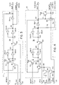
- FIG 4 there is shown a schematic circuit diagram of one of the second counter cell or stages 14 for use in each of the blocks 14-1, 14-2 and 14-3 of the counter circuit 10 in Figure 2 of the present invention.
- the counter stage 14 includes a first clocked half-latch 32, a second clocked half-latch 34, and an inverter INV1, a transmission gate TG, a pull-up P-channel MOS transistor P1, a reset P-channel MOS transistor P2, an inhibit P-channel MOS transistor P3 and a discharge N-channel MOS transistor N1.
- the first clocked half-latch 32 consists of a first N-channel pass transistor N2 and inverters INV2, INV3.
- the transistor N2 has its drain connected to a node 36 and to the input of the inverter INV2.
- the gate of the transistor N2 is connected to a charge/discharge node 38.
- the output of the inverter INV2 is connected to a node 40 and to the input of the inverter INV3.
- the output of the inverter INV3 is connected to the input of the inverter INV2.
- the source of the transistor N2 is connected to the output of the inverter INV1 at output node 42.
- the second clocked half-latch 34 consists of a second N-channel pass transistor N3, and inverters INV4, INV5.
- the transistor N3 has its drain connected to a node 44 and to the input of the inverter INV4.
- the gate of the transistor N3 is connected to the input terminal I2 for receiving the second clock phase signal PH2.
- the output of the inverter INV4 is connected to a node 46 and to the input of the inverter INV5.
- the output of the inverter INV5 is connected to the input of the inverter INV4.
- the source of the transistor N3 is connected to the output of the inverter INV2 at the node 40.
- Each of the inverters INV1 through INV5 is a conventional CMOS inverter comprised of a P-channel MOS transistor and an N-channel MOS transistor whose gate electrodes are connected together to define its input and whose drains are connected together to form its output.
- the transmission gate TG is formed of a P-channel MOS transistor P4 and an N-channel MOS transistor N4.
- the sources of the transistors P4 and N4 are connected to its input node 48, and the drains thereof are connected to its output node 50.
- the input node 48 is tied to the input terminal I5 for receiving the input complement signal ICMPL.
- the output node 50 is joined to the output terminal 02 (line 18) for providing the output complement signal OCMPL to the next stage.
- the gate electrode of the transistor P4 is connected to the output of the inverter INV4 at the node 46, and the gate electrode of the transistor N4 is connected to the output of the inverter INV1 at the output node 42.
- the pull-up transistor P1 has its source connected to a supply potential VCC, which is typically at +5.0 volts, and its drain connected to the output terminal 02 (line 18) at the node 50.
- VCC supply potential
- the gate of the transistor P1 is also connected to the output node 42.
- the reset transistor P2 has its source connected to the supply potential VCC and its drain connected to the node 36.
- the gate of the transistor P2 is connected to the input terminal I3 for receiving the complement RESETL of the reset signal.
- the inhibit transistor P3 has its drain connected to the charge/discharge node 38 and its source connected to the input terminal I4 for receiving the complement PH1L of the first clock phase signal.
- the gate of the transistor P3 is connected to the input terminal I5 via the node 48 for receiving the input complement signal ICMPL.
- the discharge transistor N1 has its drain connected to the charge ⁇ discharge node 38 and its source connected to a ground potential.
- the gate of the transistor N1 is connected to the input of terminal I4 for receiving the complement PH1L of the first clock phase signal.
- FIG 3 of the drawings there is illustrated a schematic circuit diagram of the first counter stage 12 of the counter circuit 10 of Figure 2 of the present invention.
- the first counter stage 12 of Figure 3 is quite similar to the second counter stage 14 of Figure 4, with like parts being designated by the same reference numerals.
- the discharge transistor N1 and the inhibit transistor P4 in Figure 4 have been omitted since the counter stage 12 being the least significant bit is always toggled for each cycle of the clock phase signal PH1, as was previously pointed out.
- the gate of the pass transistor N2 is connected directly to the input terminal I1 so as to receive the first clock phase signal PH1.
- FIGs 5(a) through 5(g) are timing diagrams which are useful in understanding the operation of the 4-bit up-counter circuit 10 of Figure 2.
- the reset signal RESET applied to the input terminal 28 is at a logic "1" level prior to time t0 ⁇ .
- the transmission gate T1 is open so that the first clock phase signal PH1 is prevented from being applied to the input terminals I1 of the counter stages 12 and 14.
- This reset signal RESET is also inverted by the inverter T3 so as to apply a low or "0 ⁇ " logic level to the gates of the reset transistors P2 in the counter stages 12 ( Figure 3) and 14 ( Figure 4).
- the input complement signal on the output line 16 to the second stage 14-1 will be at a high logic level.
- the input complement signal on the respective lines 18-1 and 18-2 from the second counter stages 14-1 and 14-2 will also be at the high logic level since all the pull-up transistors P1 will be rendered conductive.
- the reset signal RESET makes a high-to-low transition which closes the transmission gate T1 in order to initialize the counting.
- the half-latch 34 will be transparent so as to allow the high logic level at the node 40, which is passed through the pass transistor N3, to reach the output of the inverter INV4. Due to the inverter INV4, the node 46 will be at a low logic level. Further, this low logic level will be inverted again by the inverter INV1 so as to toggle the output bit D at time t2a, as shown in Figure 5(f).
- the high level of the second clock phase signal PH2 will also cause the output bit C to be toggled to a high level at the same time t4a, as shown in Figure 5(e).
- a complement PH1L (not shown) of the first clock phase signal will also be high.
- the charge/discharge node 38 will be discharged.
- the present invention provides an improved counter cell which includes a latch circuit, a control circuit, and a pull-up circuit. Further, any number of such counter cells may be connected to form an N-bit counter circuit, the counter cells being constructed with a relatively small number of components so as to reduce the required amount of chip area.
Abstract
Description
- This invention relates generally to semiconductor integrated circuit devices and more particularly, it relates to an improved counter circuit formed of a plurality of substantially identical bit cells in which each bit cell is fabricated with a smaller number of components than has been traditionally available.
- As is generally well known in the art, one of the most common ways to synchronize events occurring in digital logic circuitry is achieved by utilizing conventional counter circuits. These counter circuits are typically adapted to count up to a certain number of clock pulses. Further, such counter circuits may be operated on straight binary counting codes, Gray codes, or any other suitable code arrangement. Dependent upon the range of the counter circuit desired, there is determined the number of counter cells or stages to be required. Each of the counter cells corresponds to one bit of the counter circuit.
- In the normal binary counting operation of an up-counter, prior to starting of the counting circuit a reset signal is supplied to each of the counter cells so that each bit will be initially set to "zero." Thereafter, at each cycle of the clock pulses the counter circuit will count up by one. For example, in the case of a 4-bit counter circuit, when the reset signal is applied the values of the four bits will be set to 0̸0̸0̸0̸. Then, after each cycle of the clock pulses following the reset signal, the values of the four bits will be changed to: 0̸0̸0̸1, 0̸0̸10̸, 0̸0̸11, and so on.
- At the present time, most of the prior art counter circuits employ two-phase clocking signals or pulses, with a carry chain. At each cycle of the clock pulses, the values of the carry-in signal and the current state of a particular bit are used to determine the next output state of the particular bit and to generate a carry-out signal. Generally, a logic "AND" function is used to generate the carry-out signal, and a logic "EXCLUSIVE OR" function is performed on the carry-in signal and the current state of the particular bit so as to output the new or next state of the particular bit. A prior
art counter cell 2 utilizing this technique is shown in Figure 1. As can be seen, this approach requires the use of twenty-four (24) MOS transistors. Since a relatively large number of components is used in this implementation of each counter cell, there is required the need of increased amounts of chip area, which not only increases manufacturing costs but also adds to the amount of power dissipation. - It would therefore be desirable to provide an improved counter circuit which contains a plurality of substantially identical bit cells, each cell being formed with a smaller number of components than has been traditionally required. Further, it also would be expedient to construct each bit cell to be of regular configuration or structure so as to conform to a repeatable pattern suitable for very large scale integration (VLSI) with high packing density.
- Patent Abstracts of Japan, Vol. 10, No. 221, discloses a counter cell comprising a latch for storing a binary output signal, the latch being formed of a first clocked half-latch having an input and an output, a second clocked half-latch having its input connected to the output of the first clocked half-latch and an output, and an inverter having its input connected to the output of the second clocked half-latch and its output connected to the input of the first clocked half-latch; the first clocked half-latch being responsive to a first clock phase signal for transferring the binary output signal from its input to its output, the second clocked half-latch being responsive to a second clock phase signal for transferring the binary output signal from its input to its output.
- According to the present invention such a cell is characterized by control circuit means responsive to an input complement signal for selectively passing the first clock phase signal to the first clocked half-latch so as to permit toggling the state of the binary output signal; and pull-up means responsive to the binary output signal and the input complement signal for generating an output complement signal, the logic value of the output complement signal being equal to the logic value of the input complement signal only when the binary output signal is at a high logic level whereby the logic value of the output complement signal is maintained at a high logic level when the binary output signal is at a low logic level.
- Accordingly, we describe an improved counter circuit which is relatively simple and economical to manufacture and assemble.
- We further describe an improved counter cell which is formed of a relatively smaller number of components, thereby reducing IC chip size and power dissipation.
- The improved counter circuit is formed of a plurality of substantially identical bit cells or stages in which each bit cell thereof has a regular structure suitable for very large scale integration.
- In one example of the invention, a plurality of the counter cells are arranged to form an N-bit up-counter. In another example of the present invention, the counter cells are arranged to form a 4-bit up-counter.
- In the accompanying drawings, by way of example only:
- Figure 1 is a schematic circuit diagram of a prior art counter cell;
- Figure 2 is a block diagram of a 4-bit counter circuit embodying the present invention;
- Figure 3 is a schematic circuit diagram of a counter cell for use in the least significant
bit counter stage 12 of Figure 2; - Figure 4 is a schematic circuit diagram of a counter cell embodying the present invention for use in the
counter cells 14 of Figure 2; and - Figures 5(a)-5(g) are timing diagrams useful in understanding the operation of the counter circuit of Figure 2.
- Referring now in detail to the drawings, there is shown in Figure 2 a block diagram of a
counter circuit 10. Thecounter circuit 10 includes a first counter cell orstage 12 for the least significant bit (LSB) and a plurality of identical second counter cells or stages 14-1, 14-2 and 14-3 for the remaining bits. Dependent on the desired range of the counter circuit, it should be understood to those skilled in the art that this determines the number of identicalsecond counter stages 14 required. Thecounter circuit 10 of Figure 2 comprises a 4-bit up-counter which is exemplary of the present invention. Thus, thecounter circuit 10 includes onefirst counter stage 12 and three identicalsecond counter stages 14 designated as 14-1, 14-2 and 14-3. - Each of the
counter stages counter stages - The
first counter stage 12 includes three input signals consisting of a first input clock phase signal PH1 on input terminal I1, a second input clock phase signal PH2 on input terminal I2, and the complement of a reset signal RESETL oninput terminal 13. Thecounter stage 12 provides two output signals consisting of an output bit signal OUT on a first output terminal O1, which represents the least significant bit D, and an output complement signal OCMPL on a second output terminal O2 connected toline 16. - Each of the three second counter stages 14-1, 14-2 and 14-3 receives not only the same three input signals PH1, PH2 and RESETL, but it also receives the complement of PH1, PH1L, on input terminal I4 and an input complement signal ICMPL on input terminal I5. The counter stages 14-1, 14-2 and 14-3 also provides corresponding output complement signals OCMPL on the second output terminals O2 connected to lines 18-1, 18-2 and 18-3, respectively. It will be noted that the input terminal I5 of each counter stage 14-1, 14-2 and 14-3 is connected to receive the corresponding output complement signal OCMPL via the
lines 16, 18-1 and 18-2 of the preceding counter stage. The output complement signal OCMPL on line 18-3 of the last counter stage 14-3 is left unconnected. The counter stages 14-1, 14-2 and 14-3 also generate output bit signals OUT on their output terminal O1 for the bits C, B and A, wherein the output terminal O1 for the bit A represents the most significant bit (MSB). - The
counter stage 10 further includes acontrol section 20 formed of a transmission gate T1, an N-channel MOS transistor T2, and a pair of inverters T3, T4. The transmission gate T1 is formed of a P-channel MOS transistor and an N-channel MOS transistor. The sources of the P-channel and N-channel transistors are connected to itsinput node 22, and the drains thereof are connected to itsoutput node 24. Theinput node 22 is tied to aninput terminal 25 for receiving the first clock phase signal PH1. The gate electrode of the P-channel transistor is joined to a control node 26 which is connected to aninput terminal 28 for receiving the reset signal RESET. The gate electrode of the N-channel transistor is joined to acontrol node 30 and to the output of the inverter T3. The input of the inverter T3 is also connected to theinput terminal 28 for receiving the reset signal RESET. The output of the inverter T3 defining the complement RESETL of the reset signal is also fed to the input terminals I3 of therespective counter stages - The control node 26 is also connected to the gate electrode of the transistor T2. The transistor T2 has its drain electrode connected to the
output node 24 of the transmission gate T1 and has its source electrode connected to a ground potential. Theoutput node 24 of the transmission gate T1 is also fed to the input terminals I1 of thecounter stages input terminal 32 is applied to the input terminals I2 of thecounter stages - The operation of counter circuits is well known in the art. While various types of code arrangements may be used, the typically binary code pattern is illustrated in the Table listed below. The code pattern in the Table is directed to a 4-bit, up-counter operation which provides sixteen counts (0̸-15).
T A B L E Counting Sequence of Operation COUNT Column Bit A B C D 0̸ 0̸ 0̸ 0̸ 0̸ 1 0̸ 0̸ 0̸ 1 2 0̸ 0̸ 1 0̸ 3 0̸ 0̸ 1 1 4 0̸ 1 0̸ 0̸ 5 0̸ 1 0̸ 1 6 0̸ 1 1 0̸ 7 0̸ 1 1 1 8 1 0̸ 0̸ 0̸ 9 1 0̸ 0̸ 1 10 1 0̸ 1 0̸ 11 1 0̸ 1 1 12 1 1 0̸ 0̸ 13 1 1 0̸ 1 14 1 1 1 0̸ 15 1 1 1 1 - In order to achieve the same functionality of the
counter cell 2 of Figure 1 with the use of a smaller number of circuit components, the updating or toggling of the current value of a particular counter cell or bit is permitted selectively to occur only when it is needed. In other words, it can be observed from the Table above that the least significant bit (LSB) in Column D toggles or changes on each count operation. That is, the column bit D is alternately 0̸, 1, 0̸, 1 and so on. It is also noted that for any count which includes all binary 1's in consecutive bit positions beginning from the least significant bit position the next higher bit position will toggle on the next count operation. For example, at count 3 (0̸0̸11) the least significant bit in column bit D and the next least significant bit in column bit C are both "1's." As a result, on the next count operation (count 4), the bits in both columns D and C toggle and the next higher bit position in column B will also toggle (from 0̸ to 1). A similar situation occurs at count 7 (0̸111) and at count 15 (1111). Therefore, it can be seen that the most significant bit in column bit A will change its state only once during the entire range of counts (0̸ - 15). - In Figure 4, there is shown a schematic circuit diagram of one of the second counter cell or stages 14 for use in each of the blocks 14-1, 14-2 and 14-3 of the
counter circuit 10 in Figure 2 of the present invention. In this schematic circuit diagram, the input and output terminals which are similar to those shown in Figure 2 are similarly numbered or labeled. Thecounter stage 14 includes a first clocked half-latch 32, a second clocked half-latch 34, and an inverter INV1, a transmission gate TG, a pull-up P-channel MOS transistor P1, a reset P-channel MOS transistor P2, an inhibit P-channel MOS transistor P3 and a discharge N-channel MOS transistor N1. - The first clocked half-
latch 32 consists of a first N-channel pass transistor N2 and inverters INV2, INV3. The transistor N2 has its drain connected to anode 36 and to the input of the inverter INV2. The gate of the transistor N2 is connected to a charge/discharge node 38. The output of the inverter INV2 is connected to anode 40 and to the input of the inverter INV3. The output of the inverter INV3 is connected to the input of the inverter INV2. The source of the transistor N2 is connected to the output of the inverter INV1 atoutput node 42. The second clocked half-latch 34 consists of a second N-channel pass transistor N3, and inverters INV4, INV5. The transistor N3 has its drain connected to anode 44 and to the input of the inverter INV4. The gate of the transistor N3 is connected to the input terminal I2 for receiving the second clock phase signal PH2. The output of the inverter INV4 is connected to anode 46 and to the input of the inverter INV5. The output of the inverter INV5 is connected to the input of the inverter INV4. The source of the transistor N3 is connected to the output of the inverter INV2 at thenode 40. Each of the inverters INV1 through INV5 is a conventional CMOS inverter comprised of a P-channel MOS transistor and an N-channel MOS transistor whose gate electrodes are connected together to define its input and whose drains are connected together to form its output. - The transmission gate TG is formed of a P-channel MOS transistor P4 and an N-channel MOS transistor N4. The sources of the transistors P4 and N4 are connected to its
input node 48, and the drains thereof are connected to itsoutput node 50. Theinput node 48 is tied to the input terminal I5 for receiving the input complement signal ICMPL. Theoutput node 50 is joined to the output terminal 02 (line 18) for providing the output complement signal OCMPL to the next stage. The gate electrode of the transistor P4 is connected to the output of the inverter INV4 at thenode 46, and the gate electrode of the transistor N4 is connected to the output of the inverter INV1 at theoutput node 42. The pull-up transistor P1 has its source connected to a supply potential VCC, which is typically at +5.0 volts, and its drain connected to the output terminal 02 (line 18) at thenode 50. The gate of the transistor P1 is also connected to theoutput node 42. - The reset transistor P2 has its source connected to the supply potential VCC and its drain connected to the
node 36. The gate of the transistor P2 is connected to the input terminal I3 for receiving the complement RESETL of the reset signal. The inhibit transistor P3 has its drain connected to the charge/discharge node 38 and its source connected to the input terminal I4 for receiving the complement PH1L of the first clock phase signal. The gate of the transistor P3 is connected to the input terminal I5 via thenode 48 for receiving the input complement signal ICMPL. The discharge transistor N1 has its drain connected to the charge\discharge node 38 and its source connected to a ground potential. The gate of the transistor N1 is connected to the input of terminal I4 for receiving the complement PH1L of the first clock phase signal. - In Figure 3 of the drawings, there is illustrated a schematic circuit diagram of the
first counter stage 12 of thecounter circuit 10 of Figure 2 of the present invention. It will be noted that thefirst counter stage 12 of Figure 3 is quite similar to thesecond counter stage 14 of Figure 4, with like parts being designated by the same reference numerals. As can be seen, the discharge transistor N1 and the inhibit transistor P4 in Figure 4 have been omitted since thecounter stage 12 being the least significant bit is always toggled for each cycle of the clock phase signal PH1, as was previously pointed out. Thus, the gate of the pass transistor N2 is connected directly to the input terminal I1 so as to receive the first clock phase signal PH1. Further, it can be seen that the pull-up transistor P1 and the transmission gate TG in Figure 4 have also been eliminated since the least significant bit does not receive an input complement signal ICMPL and the output of the inverter I4 at thenode 46 provides the output complement signal OCMPL on theoutput line 16 for thecounter stage 12. - Figures 5(a) through 5(g) are timing diagrams which are useful in understanding the operation of the 4-bit up-
counter circuit 10 of Figure 2. In describing the counting sequence of the counter circuit of Figure 2, reference will also be made simultaneously to Figures 3 and 4. As can be seen from Figure 5(g), the reset signal RESET applied to theinput terminal 28 is at a logic "1" level prior to time t0̸. Thus, the transmission gate T1 is open so that the first clock phase signal PH1 is prevented from being applied to the input terminals I1 of the counter stages 12 and 14. This reset signal RESET is also inverted by the inverter T3 so as to apply a low or "0̸" logic level to the gates of the reset transistors P2 in the counter stages 12 (Figure 3) and 14 (Figure 4). This ensures that the output bits ABCD will be reset to store all zeroes (0̸0̸0̸0̸) before the counting operation is permitted to begin. Accordingly, the input complement signal on theoutput line 16 to the second stage 14-1 will be at a high logic level. Further, the input complement signal on the respective lines 18-1 and 18-2 from the second counter stages 14-1 and 14-2 will also be at the high logic level since all the pull-up transistors P1 will be rendered conductive. - At time t0̸, the reset signal RESET makes a high-to-low transition which closes the transmission gate T1 in order to initialize the counting. When the first clock phase signal PH1 goes high at time t1, as illustrated in Figure 5(a), the half-latch 32 (Figure 3) will be transparent so as to permit the low logic level at the output of the inverter INV1 (bit D = 0̸), which is passed through the pass transistor N2, to reach the output of the inverter INV2 at the
node 40. Due to the inverter INV2, thenode 40 will be at a high or "1" logic level. It should be noted that this high level of the first clock phase signal PH1 at the time t1 does not reach the gates of the corresponding pass transistors N2 (Figure 4) in the counter stages 14-1 through 14-3 since the input complement signal ICMPL on the respective input terminals I5 will be at the high level, thereby rendering the inhibit transistor P3 to be nonconductive. Consequently, the output bits B, C and D will remain unchanged. - Referring back to Figure 3 again, when the second clock phase signal PH2 goes high at time t2, as depicted in Figure 5(b), the half-
latch 34 will be transparent so as to allow the high logic level at thenode 40, which is passed through the pass transistor N3, to reach the output of the inverter INV4. Due to the inverter INV4, thenode 46 will be at a low logic level. Further, this low logic level will be inverted again by the inverter INV1 so as to toggle the output bit D at time t2a, as shown in Figure 5(f). As a result, the output state of thecounter stage 12 will be D = 1 and the output complement signal OCMPL on theline 16 will be at a low logic level, which is the input complement signal ICMPL for the counter stage 14-1. Therefore, the output bits ABCD will be 0̸0̸0̸1 at the time t2a, which are illustrated in respective Figure 5(c) through 5(f). - At time t3 when the next first clock phase signal PH1 goes high, the output bit D being high will again be passed to the node 40 (Figure 3). At time t4 when the next second clock phase signal PH2 goes high, the output bit D will be toggled to a low logic level at time t4a (Figure 5(f)). Simultaneously, at the time t3 the high level of the first clock phase signal PH1 will also be transferred to the gate of the pass transistors N2 (node 38) in the counter stage 14-1 (Figure 4) since its input complement signal will be at a low logic level, thereby rendering the input transistor P3 to be conductive. As a result, the output bit C being low will be passed to the node 40 (Figure 4). At the time t4, the high level of the second clock phase signal PH2 will also cause the output bit C to be toggled to a high level at the same time t4a, as shown in Figure 5(e). Thus, the output state of the counter stage 14-1 will be C = 1 and the output complement signal OCMPL on the line 18-1 will be equal to the input complement signal ICMPL on the
line 16 from thecounter stage 12 since the transistor P1 (Figure 4) will be turned off and the transmission gate TG will be closed. It should be noted that when the second clocked phase signal PH2 is high a complement PH1L (not shown) of the first clock phase signal will also be high. Hence, on every cycle of the complement PH1L of the first clock phase signal the charge/discharge node 38 will be discharged. - It should be apparent to those skilled in the art that a similar analysis can be made on the counter stages 12 and 14 in the counter circuit of Figure 2 for each of the subsequent cycles of the clock phase signal PH1 in order to obtain the corresponding states of the output bits ABCD illustrated in Figures 5(c)-5(f), respectively. It should also be clear that the input complement signal ICMPL functions as a control signal to determine whether or not to complement or change (toggle) the current state of a particular output bit in the counter stages 14-1, 14-2 and 14-3. If ICMPL = 0̸, then the particular bit will be allowed to toggle. If ICMPL = 1, then this particular bit will be prohibited from changing its state and will remain in its present state. By using this approach, the number of circuit components that have been used for implementing each of the counter stages 14 have been reduced. In comparing Figure 4 of the
present counter cell 14 with the prior artcounter cell 2 of Figure 1, it can be seen that there is a saving of six transistors per cell. - From the foregoing detailed description, it can thus be seen that the present invention provides an improved counter cell which includes a latch circuit, a control circuit, and a pull-up circuit. Further, any number of such counter cells may be connected to form an N-bit counter circuit, the counter cells being constructed with a relatively small number of components so as to reduce the required amount of chip area.
Claims (14)
- A counter cell comprising:latch means for storing a binary output signal;said latch means being formed of a first clocked half-latch (32) having an input and an output, a second clocked half-latch (34) having its input connected to the output of said first clocked half-latch and an output, and an inverter (INV1) having its input connected to the output of said second clocked half-latch and its output connected to the input of said first clocked half-latch;said first clocked half-latch (32) being responsive to a first clock phase signal for transferring the binary output signal from its input to its output, said second clocked half-latch (34) being responsive to a second clock phase signal for transferring the binary output signal from its input to its output;characterised by control circuit means (P3) responsive to an input complement signal for selectively passing the first clock phase signal to said first clocked half-latch so as to permit toggling the state of said binary output signal; and
pull-up means (P1, TG) responsive to said binary output signal and said input complement signal for generating an output complement signal, the logic value of said output complement signal being equal to the logic value of said input complement signal only when said binary output signal is at a high logic level whereby the logic value of said output complement signal is maintained at a high logic level when said binary output signal is at a low logic level. - A counter cell as claimed in claim 1, wherein said first clocked half-latch (32) is formed of a first pass transistor (N2) and first and second inverters (INV2, INV3).
- A counter cell as claimed in claim 2, wherein said second clocked half-latch (34) is formed of a second pass transistor (N3) and third and fourth inverters (INV4, INV5).
- A counter cell according to claim 3 further comprising:a fifth inverter (INV1) having an input and an output for storing a bit signal at a first output terminal;said first pass transistor (N2) having its source connected to the output of said fifth inverter (INV1) and its drain connected to the input of said first inverter (INV2), said first inverter (INV2) having its output connected to the input of said second inverter (INV3), said second inverter (INV3) having its output connected to the input of said first inverter (INV2);said second pass transistor (N3) having its source connected to the output of said first inverter (INV2) and its drain connected to the input of said third inverter (INV4), said third inverter (INV4) having its output connected to the input of said fourth inverter (INV5), said fourth inverter (INV5) having its output connected to the input of said third inverter (INV4).
- A counter cell according to claim 3 or claim 4 wherein the control circuit means comprises an inhibit transistor (P3) having its source connected to a first input terminal for receiving the first clock phase signal and its drain connected to the gate of said first pass transistor (N2) at a charge/discharge node (38), said gate of said second pass transistor (N3) being connected to a second input terminal for receiving the second clock phase signal, said gate of said inhibit transistor (P3) being connected to a third input for receiving the input complement signal.
- A counter cell according to claim 5 and further comprising a discharge transistor (N1) having its drain connected to the charge/discharge node (38) and its source connected to a ground potential, the gate of said discharge transistor (N1) being connected to a fourth input terminal for receiving the complement of said first clock phase signal.
- A counter cell according to claim 5 or claim 6 wherein the pull-up means comprises a transmission gate (TG) and a pull-up transistor (P1), the transmission gate (TG) being formed of a P-channel transistor (P4) and an N-channel transistor (N4) whose sources are connected to the gate of said inhibit transistor (P3) and whose drains are connected to a second output terminal to provide an output complement signal, said P-channel transistor (P4) having its gate connected to the output of said third inverter (INV4) and said N-channel transistor (N4) having its gate connected to the first output terminal; and
the pull-up transistor (P1) having its source connected to a supply potential and its drain connected to the second output terminal, the gate of said pull-up transistor (P1) being connected to the first output terminal. - A counter cell as claimed in claim 7, further comprising a reset transistor (P2) having its source connected to the supply potential, and its drain connected to the input of said first inverter (INV2), the gate of said reset transistor (P2) being connected to a fifth input terminal for receiving the complement of a reset signal.
- A counter cell as claimed in claim 7, wherein said first and second pass transistors (N2, N3) and said discharge transistor (N1) are comprised of N-channel MOS transistors.
- A counter cell as claimed in claim 7, wherein said pull-up, reset, and inhibit transistors (P1-P3) are comprised of P-channel MOS transistors.
- A counter cell as claimed in claim 4, wherein said inverters (INV1-INV5) are comprised of CMOS inverters, each being formed of a P-channel transistor and an N-channel transistor.
- An N-bit counter formed by connecting together a plurality of counter cells, each cell comprising a cell according to any one of the preceding claims.
- An N-bit counter according to claim 12 wherein said counter cells are connected together to form a 4-bit up-counter circuit.
- A counter circuit formed of a plurality of counter stages, each counter stage except for the least significant bit stage comprising a counter cell according to any one of the preceding claims.
Applications Claiming Priority (2)
| Application Number | Priority Date | Filing Date | Title |
|---|---|---|---|
| US07/678,510 US5175753A (en) | 1991-04-01 | 1991-04-01 | Counter cell including a latch circuit, control circuit and a pull-up circuit |
| US678510 | 1991-04-01 |
Publications (3)
| Publication Number | Publication Date |
|---|---|
| EP0507441A2 EP0507441A2 (en) | 1992-10-07 |
| EP0507441A3 EP0507441A3 (en) | 1994-02-16 |
| EP0507441B1 true EP0507441B1 (en) | 1997-10-22 |
Family
ID=24723089
Family Applications (1)
| Application Number | Title | Priority Date | Filing Date |
|---|---|---|---|
| EP92301612A Expired - Lifetime EP0507441B1 (en) | 1991-04-01 | 1992-02-26 | Counter circuit |
Country Status (5)
| Country | Link |
|---|---|
| US (1) | US5175753A (en) |
| EP (1) | EP0507441B1 (en) |
| JP (1) | JPH07202682A (en) |
| AT (1) | ATE159629T1 (en) |
| DE (1) | DE69222798T2 (en) |
Families Citing this family (8)
| Publication number | Priority date | Publication date | Assignee | Title |
|---|---|---|---|---|
| FR2692072A1 (en) * | 1992-06-05 | 1993-12-10 | Sgs Thomson Microelectronics | Bistable scale with reset command. |
| US5287394A (en) * | 1993-03-22 | 1994-02-15 | Advanced Micro Devices, Inc. | Fast counter with uniform delay structures |
| JPH07183771A (en) * | 1993-12-22 | 1995-07-21 | Fujitsu Ltd | Flip-flop circuit |
| US5495513A (en) * | 1994-11-18 | 1996-02-27 | Advanced Micro Devices Inc. | Counter cell and counter circuit |
| WO1997020268A1 (en) * | 1995-11-27 | 1997-06-05 | Philips Electronics N.V. | A parametrizable control module comprising first and second loadables counters, an electronic circuit comprising a plurality of such parametrized control modules, and a method for synthesizing such circuit |
| US5742182A (en) * | 1996-06-13 | 1998-04-21 | Sun Microsystems, Inc. | Symmetric selector circuit for event logic |
| US6753705B1 (en) * | 2000-07-27 | 2004-06-22 | Sigmatel, Inc. | Edge sensitive detection circuit |
| DE10353501B4 (en) * | 2003-11-11 | 2006-05-18 | Technische Universität Dresden | Counter circuit and frequency divider stage |
Family Cites Families (7)
| Publication number | Priority date | Publication date | Assignee | Title |
|---|---|---|---|---|
| US3657557A (en) * | 1970-10-19 | 1972-04-18 | Gen Instrument Corp | Synchronous binary counter |
| US4025800A (en) * | 1975-06-16 | 1977-05-24 | Integrated Technology Corporation | Binary frequency divider |
| JPS52146162A (en) * | 1976-05-29 | 1977-12-05 | Toshiba Corp | Programmable counter |
| US4512030A (en) * | 1983-01-28 | 1985-04-16 | Motorola, Inc. | High speed presettable counter |
| DE3428393A1 (en) * | 1984-08-01 | 1986-02-13 | Siemens AG, 1000 Berlin und 8000 München | Clock-controlled bistable circuit |
| JPS6156512A (en) * | 1984-08-27 | 1986-03-22 | Nec Corp | Counter circuit |
| US4882505A (en) * | 1986-03-24 | 1989-11-21 | International Business Machines Corporation | Fully synchronous half-frequency clock generator |
-
1991
- 1991-04-01 US US07/678,510 patent/US5175753A/en not_active Expired - Lifetime
-
1992
- 1992-02-26 EP EP92301612A patent/EP0507441B1/en not_active Expired - Lifetime
- 1992-02-26 AT AT92301612T patent/ATE159629T1/en not_active IP Right Cessation
- 1992-02-26 DE DE69222798T patent/DE69222798T2/en not_active Expired - Fee Related
- 1992-03-31 JP JP4077148A patent/JPH07202682A/en not_active Withdrawn
Also Published As
| Publication number | Publication date |
|---|---|
| DE69222798T2 (en) | 1998-05-14 |
| US5175753A (en) | 1992-12-29 |
| DE69222798D1 (en) | 1997-11-27 |
| ATE159629T1 (en) | 1997-11-15 |
| EP0507441A2 (en) | 1992-10-07 |
| JPH07202682A (en) | 1995-08-04 |
| EP0507441A3 (en) | 1994-02-16 |
Similar Documents
| Publication | Publication Date | Title |
|---|---|---|
| US3818452A (en) | Electrically programmable logic circuits | |
| US5302866A (en) | Input circuit block and method for PLDs with register clock enable selection | |
| US6924671B2 (en) | General-purpose logic module and cell using the same | |
| EP0507441B1 (en) | Counter circuit | |
| JPS589613B2 (en) | counter pattern | |
| EP0266866B1 (en) | Dual mode-increment/decrement n-bit counter register | |
| US5532634A (en) | High-integration J-K flip-flop circuit | |
| US5495513A (en) | Counter cell and counter circuit | |
| JP2749185B2 (en) | Composite logic circuit | |
| EP0365224A2 (en) | Two phase non-overlapping clock counter circuit to be used in I.C. | |
| US4752901A (en) | Arithmetic logic unit utilizing strobed gates | |
| US4631425A (en) | Logic gate circuit having P- and N- channel transistors coupled in parallel | |
| US4891534A (en) | Circuit for comparing magnitudes of binary signals | |
| US3596108A (en) | Fet logic gate circuits | |
| US4798980A (en) | Booth's conversion circuit | |
| EP0354534B1 (en) | Semiconductor logic circuit | |
| US5287394A (en) | Fast counter with uniform delay structures | |
| CA1109128A (en) | Ternary logic circuits with cmos integrated circuits | |
| KR940000267B1 (en) | Serial comparator ic | |
| KR100236722B1 (en) | N-bit zero detecting circuit | |
| KR100278992B1 (en) | Full adder | |
| EP0250174B1 (en) | Incrementer and decrementer | |
| JPS6182527A (en) | Pulse generating circuit | |
| KR100200762B1 (en) | 1-bit full adder | |
| US5446401A (en) | Synchronous dual word decoding using PLA |
Legal Events
| Date | Code | Title | Description |
|---|---|---|---|
| PUAI | Public reference made under article 153(3) epc to a published international application that has entered the european phase |
Free format text: ORIGINAL CODE: 0009012 |
|
| AK | Designated contracting states |
Kind code of ref document: A2 Designated state(s): AT BE CH DE DK ES FR GB GR IT LI LU NL PT SE |
|
| PUAL | Search report despatched |
Free format text: ORIGINAL CODE: 0009013 |
|
| AK | Designated contracting states |
Kind code of ref document: A3 Designated state(s): AT BE CH DE DK ES FR GB GR IT LI LU NL PT SE |
|
| 17P | Request for examination filed |
Effective date: 19940721 |
|
| 17Q | First examination report despatched |
Effective date: 19960308 |
|
| GRAG | Despatch of communication of intention to grant |
Free format text: ORIGINAL CODE: EPIDOS AGRA |
|
| GRAH | Despatch of communication of intention to grant a patent |
Free format text: ORIGINAL CODE: EPIDOS IGRA |
|
| GRAH | Despatch of communication of intention to grant a patent |
Free format text: ORIGINAL CODE: EPIDOS IGRA |
|
| GRAA | (expected) grant |
Free format text: ORIGINAL CODE: 0009210 |
|
| AK | Designated contracting states |
Kind code of ref document: B1 Designated state(s): AT BE CH DE DK ES FR GB GR IT LI LU NL PT SE |
|
| PG25 | Lapsed in a contracting state [announced via postgrant information from national office to epo] |
Ref country code: IT Free format text: LAPSE BECAUSE OF FAILURE TO SUBMIT A TRANSLATION OF THE DESCRIPTION OR TO PAY THE FEE WITHIN THE PRE;WARNING: LAPSES OF ITALIAN PATENTS WITH EFFECTIVE DATE BEFORE 2007 MAY HAVE OCCURRED AT ANY TIME BEFORE 2007. THE CORRECT EFFECTIVE DATE MAY BE DIFFERENT FROM THE ONE RECORDED.SCRIBED TIME-LIMIT Effective date: 19971022 Ref country code: DK Free format text: LAPSE BECAUSE OF NON-PAYMENT OF DUE FEES Effective date: 19971022 Ref country code: AT Free format text: LAPSE BECAUSE OF FAILURE TO SUBMIT A TRANSLATION OF THE DESCRIPTION OR TO PAY THE FEE WITHIN THE PRESCRIBED TIME-LIMIT Effective date: 19971022 Ref country code: NL Free format text: LAPSE BECAUSE OF FAILURE TO SUBMIT A TRANSLATION OF THE DESCRIPTION OR TO PAY THE FEE WITHIN THE PRESCRIBED TIME-LIMIT Effective date: 19971022 Ref country code: FR Free format text: LAPSE BECAUSE OF FAILURE TO SUBMIT A TRANSLATION OF THE DESCRIPTION OR TO PAY THE FEE WITHIN THE PRESCRIBED TIME-LIMIT Effective date: 19971022 Ref country code: LI Free format text: LAPSE BECAUSE OF FAILURE TO SUBMIT A TRANSLATION OF THE DESCRIPTION OR TO PAY THE FEE WITHIN THE PRESCRIBED TIME-LIMIT Effective date: 19971022 Ref country code: GR Free format text: LAPSE BECAUSE OF FAILURE TO SUBMIT A TRANSLATION OF THE DESCRIPTION OR TO PAY THE FEE WITHIN THE PRESCRIBED TIME-LIMIT Effective date: 19971022 Ref country code: BE Free format text: LAPSE BECAUSE OF FAILURE TO SUBMIT A TRANSLATION OF THE DESCRIPTION OR TO PAY THE FEE WITHIN THE PRESCRIBED TIME-LIMIT Effective date: 19971022 Ref country code: CH Free format text: LAPSE BECAUSE OF FAILURE TO SUBMIT A TRANSLATION OF THE DESCRIPTION OR TO PAY THE FEE WITHIN THE PRESCRIBED TIME-LIMIT Effective date: 19971022 Ref country code: ES Free format text: THE PATENT HAS BEEN ANNULLED BY A DECISION OF A NATIONAL AUTHORITY Effective date: 19971022 |
|
| REF | Corresponds to: |
Ref document number: 159629 Country of ref document: AT Date of ref document: 19971115 Kind code of ref document: T |
|
| REG | Reference to a national code |
Ref country code: CH Ref legal event code: EP |
|
| REF | Corresponds to: |
Ref document number: 69222798 Country of ref document: DE Date of ref document: 19971127 |
|
| PG25 | Lapsed in a contracting state [announced via postgrant information from national office to epo] |
Ref country code: PT Free format text: LAPSE BECAUSE OF FAILURE TO SUBMIT A TRANSLATION OF THE DESCRIPTION OR TO PAY THE FEE WITHIN THE PRESCRIBED TIME-LIMIT Effective date: 19980122 Ref country code: SE Effective date: 19980122 |
|
| PG25 | Lapsed in a contracting state [announced via postgrant information from national office to epo] |
Ref country code: LU Free format text: LAPSE BECAUSE OF NON-PAYMENT OF DUE FEES Effective date: 19980226 |
|
| EN | Fr: translation not filed | ||
| NLV1 | Nl: lapsed or annulled due to failure to fulfill the requirements of art. 29p and 29m of the patents act | ||
| REG | Reference to a national code |
Ref country code: CH Ref legal event code: PL |
|
| PLBE | No opposition filed within time limit |
Free format text: ORIGINAL CODE: 0009261 |
|
| STAA | Information on the status of an ep patent application or granted ep patent |
Free format text: STATUS: NO OPPOSITION FILED WITHIN TIME LIMIT |
|
| 26N | No opposition filed | ||
| PGFP | Annual fee paid to national office [announced via postgrant information from national office to epo] |
Ref country code: GB Payment date: 20010104 Year of fee payment: 10 |
|
| REG | Reference to a national code |
Ref country code: GB Ref legal event code: IF02 |
|
| PG25 | Lapsed in a contracting state [announced via postgrant information from national office to epo] |
Ref country code: GB Free format text: LAPSE BECAUSE OF NON-PAYMENT OF DUE FEES Effective date: 20020226 |
|
| PGFP | Annual fee paid to national office [announced via postgrant information from national office to epo] |
Ref country code: DE Payment date: 20020228 Year of fee payment: 11 |
|
| GBPC | Gb: european patent ceased through non-payment of renewal fee |
Effective date: 20020226 |
|
| PG25 | Lapsed in a contracting state [announced via postgrant information from national office to epo] |
Ref country code: DE Free format text: LAPSE BECAUSE OF NON-PAYMENT OF DUE FEES Effective date: 20030902 |