EP0505944B1 - Optischer LiNbO3 Dünnfilm-Wellenleiter und Verfahren zu seiner Herstellung - Google Patents
Optischer LiNbO3 Dünnfilm-Wellenleiter und Verfahren zu seiner Herstellung Download PDFInfo
- Publication number
- EP0505944B1 EP0505944B1 EP92104907A EP92104907A EP0505944B1 EP 0505944 B1 EP0505944 B1 EP 0505944B1 EP 92104907 A EP92104907 A EP 92104907A EP 92104907 A EP92104907 A EP 92104907A EP 0505944 B1 EP0505944 B1 EP 0505944B1
- Authority
- EP
- European Patent Office
- Prior art keywords
- linbo
- thin film
- optical waveguide
- film optical
- base layer
- Prior art date
- Legal status (The legal status is an assumption and is not a legal conclusion. Google has not performed a legal analysis and makes no representation as to the accuracy of the status listed.)
- Expired - Lifetime
Links
Images


Classifications
-
- G—PHYSICS
- G02—OPTICS
- G02B—OPTICAL ELEMENTS, SYSTEMS OR APPARATUS
- G02B6/00—Light guides; Structural details of arrangements comprising light guides and other optical elements, e.g. couplings
- G02B6/10—Light guides; Structural details of arrangements comprising light guides and other optical elements, e.g. couplings of the optical waveguide type
- G02B6/12—Light guides; Structural details of arrangements comprising light guides and other optical elements, e.g. couplings of the optical waveguide type of the integrated circuit kind
- G02B6/13—Integrated optical circuits characterised by the manufacturing method
- G02B6/131—Integrated optical circuits characterised by the manufacturing method by using epitaxial growth
Definitions
- the present invention relates to an LiNbO 3 thin film optical waveguide device and a process for producing the same.
- the device exhibits the waveguide function for ordinary ray only or for extraordinary ray only or for the light including extraordinary ray. Moreover, it absorbs short wavelength light (e.g. blue light) only a little.
- the optical waveguide of LiNbO 3 is usually formed by the metal diffusion process (which involves the step of selectively diffusing a metal such as titanium into the part where the optical waveguide is formed) or by the ion exchange (proton exchange) process.
- the foregoing first process has a disadvantage that the resulting optical waveguide is liable to optical damage on account of the introduction of impurities such as titanium.
- impurities such as titanium.
- a titanium-containing optical waveguide changes in refractive index (and hence becomes poor in characteristic properties) when it encounters a beam of intense light. Since the optical damage is more serious as the wavelength is shorter, it cannot be used for blue light in the visible region.
- the foregoing second process also has a disadvantage of deteriorating the characteristic properties (e.g., electro-optical constant and nonlinear optical constant) of LiNbO 3 . Moreover, its application is limited to an optical waveguide which is effective only for extraordinary ray.
- a conceivable way to address the foregoing problems is to form the optical waveguide by liquid phase epitaxy.
- liquid phase epitaxy it would be possible to control the depth with certainty and to create the sharp stepwise distribution of refractive indices.
- the present inventors investigated the reason why the LiNbO 3 thin film formed by liquid phase epitaxy absorbs short wavelength light. It was found that the light absorption is due to the entrance of a vanadium atom into the Nb site in the crystal of LiNbO 3 thin film. In this situation, the vanadium ion has the d electron (in the outer shell electron orbital) whose level is split by the crystal field, and transition from one level to another is the cause of light absorption in a specific wavelength region where light absorption should not occur naturally.
- U.S. Patent No. 3,998,687 discloses a process for the liquid phase epitaxy of LiNbO 3 from a molten solution of Li 2 B 2 O 4 -Li 2 Nb 2 O 6 . This process is intended to grow LiNbO 3 on an LiTaO 3 substrate by liquid phase epitaxy. The resulting LiNbO 3 does not selectively guide ordinary light only.
- the first object is solved by the device according to the teaching of appended claim 1
- the second object is solved by the method according to the teaching of appended claim 5.
- the LiNbO 3 thin film optical waveguide device was completed on the basis of the following findings.
- Fig. 1 is a schematic sectional view showing an embodiment of the LiNbO 3 thin film optical waveguide device pertaining to the present invention.
- Fig. 2 is a schematic sectional view showing an embodiment of the LiNbO 3 thin film optical waveguide device pertaining to the present invention.
- Fig. 3 is a schematic sectional view showing an embodiment of the LiNbO 3 thin film optical waveguide device pertaining to the present invention.
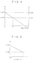
- Fig. 4 is a diagrammatic representation showing the relationship between the amount of MgO doped and the refractive indices of n o and n e .
- Fig. 5 is a diagrammatic representation showing the relationship between Li/Nb and the refractive index n e .
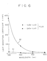
- Fig. 6 is a graph showing the dependence of the light absorption coefficient on the wavelength.
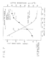
- Fig. 7 is a graph showing the dependence of the lattice mismatching and X-ray half band width on the amount of Li 2 O in the molten solution.
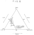
- Fig. 8 is a ternary diagram showing the relationship between the crystallinity and the amounts of Li 2 O, B 2 O 3 , and Nb 2 O 5 in the molten solution.
- Fig. 9 is a diagrammatic representation showing the relationship between the refractive index n e and the composition of the molten solution.
- the LiNbO 3 thin film optical waveguide is designed to absorb a less amount of light in the short wavelength region.
- This object is achieved by using B 2 O 3 in place of V 2 O 5 as the flux for liquid phase epitaxy.
- the LiNbO 3 thin film crystal is free from an impurity that brings about light absorption. That is, vanadium ion has the d electron (in the outer shell electron orbital) whose level is split by the crystal field, and transition from one level to another is the cause of light absorption in a specific wavelength region where light absorption should not occur naturally.
- B 2 O 3 used as the flux does not readily enter LiNbO 3 .
- the LiNbO 3 optical waveguide has the refractive indices n o and n e for ordinary ray and extraordinary ray, respectively, both of which decrease it the increasing amount of MgO doped.
- Fig. 4 shows the dependence of the refractive indices n o and n e (at a wavelength ⁇ of 633 nm) on the amount of MgO doped, with the LiNbO 3 substrate 1 having the congruent composition.
- the LiNbO 3 optical waveguide has the refractive index n e for extraordinary ray which varies depending on the atomic ratio Li/Nb of Li and Nb constituting the LiNbO 3 , whereas it also has the refractive index n o for ordinary ray which hardly depends on the atomic ratio Li/Nb.
- Fig. 5 shows the dependence of the refractive index n e for extraordinary ray (at a wavelength ⁇ of 633 nm) on the atomic ratio Li/Nb.
- the LiNbO 3 substrate 1 has refractive indices of n os and n es for ordinary ray and extraordinary ray, respectively, and the LiNbO 3 thin film formed by liquid phase epitaxy has refractive indices of n o2 and n e2 for ordinary ray and extraordinary ray, respectively, then n o2 > n os and n e2 ⁇ n es or n e2 ⁇ n es , if proper selection is made of the amount of MgO to be doped into the LiNbO 3 substrate 1, the amount of MgO or ZnO to be doped into the LiNbO 3 thin film, and the Li/Nb atomic ratio. This makes it possible to produce the special LiNbO 3 thin film optical waveguide 2 which guides ordinary ray only.
- the optical waveguide which guides ordinary ray only is less liable to optical damage.
- the LiNbO 3 thin film 2 as the optical waveguide has a better quality when formed on the MgO-doped LiNbO 3 substrate 1 by liquid phase epitaxy than when formed on an undoped LiNbO 3 substrate by liquid phase epitaxy. This, combined with the liquid phase epitaxy that employs B 2 O 3 as the flux, results in the optical waveguide device which absorbs a less amount of light in the short wavelength region.
- the optical waveguide as shown in Fig. 2 is made up of an LiNbO 3 substrate 11, a base layer 13, and a thin film optical waveguide 12, with the base layer 13 being richer in Li than the thin film optical waveguide 12.
- the thin film optical waveguide 12 has refractive indices of n o2 and n e2 for ordinary ray and extraordinary ray, respectively
- the basic layer 13 has refractive indices of n o3 and n e3 for ordinary ray and extraordinary ray, respectively
- n e2 ⁇ n es which permits the thin-film optical waveguide 12 to guide at least extraordinary ray.
- n o2 > n o3 or n o2 ⁇ n o3 > n os if proper selection is made of the dopant MgO or ZnO for the base layer 13 and the substrate 11 in relation to the LiNbO 3 thin film optical waveguide 12. In this case, the guide of ordinary ray is also accomplished by the base layer 13 and the thin film optical waveguide 12.
- the LiNbO 3 thin film optical waveguide device may have the structure as shown in Fig. 3. It is composed of an LiNbO 3 substrate 21 which is undoped or doped with MgO or ZnO, an LiNbO 3 base layer 23 which is doped with MgO so that it has low refractive indices n o3 and n e3 for ordinary ray and extraordinary ray, respectively, and an LiNbO 3 thin film optical waveguide 22 which is undoped or doped with a less amount of MgO (than in the base layer 23) or doped with a proper amount of ZnO so that it has refractive indices n o2 and n e2 for ordinary ray and extraordinary ray, respectively, where n o2 > n o3 and n e2 > n e3 , and it guides both ordinary ray and extraordinary ray.
- the LiNbO 3 thin film optical waveguide 12 (or 22) and the LiNbO 3 base layer 13 (or 23) are formed on top of the other by liquid phase epitaxy.
- This double-layer structure is advantageous over the single-layer structure in which the thin film optical waveguide 12 (or 22) is formed directly on the LiNbO 3 substrate 11 (or 21).
- the thin film optical waveguide 12 (or 22) has much stabler crystallinity and hence has optically better properties.
- the structure shown in Fig. 2 or 3 provides the base layer 13 (or 23) and the thin film optical waveguide 12 (or 22), both having the outstanding properties, if the LiNbO 3 substrate is doped with MgO or ZnO.
- An optical waveguide device which guides ordinary ray only is explained first. It is schematically shown in section in Fig. 1. There is shown an LiNbO 3 substrate 1 which is doped with MgO. On this substrate 1 is formed an LiNbO 3 thin film optical waveguide 2 (which is undoped or doped with a small amount of MgO or an adequate amount of ZnO) by liquid phase epitaxy from a molten solution in which the atomic ratio Li/Nb is higher than 0.985 (so that it has a refractive index n e smaller than that of the substrate 1) and lower than 1.04 (so that it has good crystallinity).
- the amount of MgO to be doped into the substrate 1 should be 0.1 to 10 mol%. With an amount less than 0.1 mol%, MgO hardly produces the effect of lowering the refractive index. With an amount in excess of 10 mol%, MgO has an adverse effect on the crystallinity.
- the liquid phase epitaxy for the LiNbO 3 thin film optical waveguide 2 employs Li 2 O-B 2 O 3 as the flux.
- the flux should be free from impurity atoms whose outer shell orbital susceptible to the crystal field in the LiNbO 3 thin film are unfilled with electrons.
- An LiNbO 3 substrate 1 is made ready. It is a Z substrate which is doped with 5 mol% MgO and has a single domain, with the spontaneous polarization in the direction indicated by the arrow a.
- an LiNbO 3 thin film optical waveguide 2 by liquid phase epitaxy from a molten solution which contains Li 2 O-B 2 O 3 as the flux.
- the amount of B 2 O 3 in the flux is fixed at 40 mol%, the amount of Li 2 O should be 45-52 mol% and the amount of Nb 2 O 5 should be 15-8 mol%.
- the thin film optical waveguide 2 in this example has a low absorption coefficient for the short wavelength light.
- the dependence of the light absorption coefficient ⁇ on the wavelength is shown in Fig. 6.
- the curve 61 in Fig. 6 represents the optical waveguide 2 formed by the liquid phase epitaxy which employs Li 2 O-B 2 O 3 as the flux according to Example 1, and the curve 62 in Fig. 6 represents the optical waveguide 2 formed by the liquid phase epitaxy which employs Li 2 O-V 2 O 5 as the flux according to the prior art technology.
- the spontaneous polarization occurs in the direction which coincides with that (indicated by the arrow a) of the LiNbO 3 substrate 1.
- the optical waveguide 2 be formed on the +Z surface in the production of a functional optical waveguide device.
- the LiNbO 3 thin film formed by liquid phase epitaxy has the spontaneous polarization whose direction depends on the difference between the magnitudes of spontaneous polarization of the substrate 1 and the thin film 2. If the amount of Li 2 O is less than 45 mol%, the polarization is unstable even on the +Z surface, with reversal noticed partly.
- the thin film optical waveguide 2 has the lattice mismatching ⁇ a and crystallinity which vary depending on the amount of Li 2 O in the molten solution for liquid phase epitaxy, with the amount of B 2 O 3 in the molten solution fixed at 40 mol%, as shown in Fig. 7. (The crystallinity is expressed in terms of half band width in X-ray diffractometry.)
- the curve 71 represents the lattice mismatching ⁇ a and the curve 72 represents the half band width in X-ray diffractometry. It is apparently noted that the lattice mismatching ⁇ a increases with the increasing amount of Li 2 O, whereas the X-ray half band width decreases (or the crystallinity improves) with the increasing amount of Li 2 O. When the amount of Li 2 O exceeds about 54 mol%, epitaxy is unlikely to occur. This is indicated by the fact that there are regions in which the thin film exhibits the properties of a mirror and has the good crystallinity.
- the LiNbO 3 thin film formed by liquid phase epitaxy has the crystallinity which depends on the amounts of B 2 O 3 , Li 2 O, and Nb 2 O 5 in the molten solution, as shown in Fig. 8 (ternary diagram).
- the area surrounded by lines passing through points A, B, C, and D is one in which the mirror-like LiNbO 3 thin film is obtained by liquid phase epitaxy.
- the area surrounded by lines passing through points A, E, F, and G is one in which the LiNbO 3 thin film having almost the same crystallinity as the substrate 1 is obtained.
- This example may be modified such that the LiNbO 3 thin film optical waveguide is doped with MgO or ZnO in an amount much smaller than that of MgO doped into the substrate.
- This example may also be modified such that the LiNbO 3 thin film optical waveguide 2 is formed by liquid phase epitaxy on the X surface or Y surface of the substrate 1 in place of Z surface of the substrate 1.
- the LiNbO 3 thin film optical waveguide 12 is formed on the substrate, with the LiNbO 3 base layer 13 interposed between them, so that the optical waveguide 12 guides extraordinary ray.
- the sample is prepared by forming on the LiNbO 3 substrate 11 the LiNbO 3 base layer 13 and the LiNbO 3 thin film optical waveguide 12 on top of the other.
- the LiNbO 3 base layer 13 contains more Li (or is richer in Li) than the LiNbO 3 thin film optical waveguide 12.
- An LiNbO 3 substrate 11 is made ready. It is a Z substrate which is doped with 5 mol% MgO and has a single domain, with the spontaneous polarization in the direction indicated by the arrow a.
- a base layer 13 and an LiNbO 3 thin film optical waveguide 12 by liquid phase epitaxy from a molten solution of Li 2 O-B 2 O 3 -Nb 2 O 5 which contains Li 2 O-B 2 O 3 as the flux, in the same manner as in Example 1.
- the base layer 13 is formed such that it contains more Li than the thin film optical waveguide 12.
- the base layer 13 has a refractive index n e for extraordinary ray which is smaller than that of the thin film optical waveguide 12.
- the LiNbO 3 thin film has the refractive index n e for extraordinary ray (at a wavelength of 632.8 nm) which varies depending on the molar ratio (R%) of Nb 2 O 5 to Li 2 O in the molten solution, as shown in Fig. 9.
- the chain line in Fig. 9 denotes the n e of the LiNbO 3 substrate doped with 5 mol% of MgO.
- the foregoing embodiment pertaining to the present invention is effective in guiding extraordinary ray because the Li-rich LiNbO 3 base layer 13 has a smaller refractive index for extraordinary ray than the LiNbO 3 thin film optical waveguide 12. In other words, extraordinary ray is effectively enclosed in the optical waveguide 12.
- the LiNbO 3 thin film having good crystallinity is formed by liquid phase epitaxy when the ratio R of Nb 2 O 5 /Li 2 O is about 30%, it is necessary that the content of Li in the base layer 13 be greater than that in the thin film optical waveguide 12 when the ratio R is 30% or less.
- the thin film optical waveguide 12 will be effective in guiding both ordinary ray and extraordinary ray if the amount of MgO or ZnO to be doped is properly selected so that the thin film optical waveguide 12 has a greater refractive index for ordinary ray than the base layer 13.
- FIG. 3 Another embodiment which guides both ordinary ray and extraordinary ray is explained with reference to Fig. 3.
- an LiNbO 3 substrate 21 which is undoped or doped with MgO.
- a base layer 23 doped with MgO
- an LiNbO 3 thin film optical waveguide 22 which is doped with a less amount of MgO than the base layer 23 or doped with a proper amount of ZnO so that its refractive indices n o and n e for ordinary ray and extraordinary ray, respectively, are greater than those of the base layer 23.
- An example for this embodiment is given below.
- An LiNbO 3 substrate 21 is made ready. It is a Z substrate which is doped with 5 mol% MgO and has a single domain, with the spontaneous polarization in the direction indicated by the arrow a. On the substrate are consecutively formed a base layer 23 and an LiNbO 3 thin film optical waveguide 22 by liquid phase epitaxy from a molten solution of Li 2 O-B 2 O 3 -Nb 2 O 5 which contains Li 2 O-B 2 O 3 as the flux, in the same manner as in Example 1.
- the LiNbO 3 base layer 23 and the LiNbO 3 thin film optical waveguide 22 may have the stoichiometric composition (i.e., Li/Nb ⁇ 1), and in this case the LiNbO 3 base layer alone is doped with MgO.
- An advantage of this embodiment is that the LiNbO 3 base layer 23 and the LiNbO 3 thin film optical waveguide 22 have good crystallinity and film properties when both of them have the stoichiometric composition.
- the liquid phase epitaxy employs Li 2 O-B 2 O 3 as the flux.
- the flux contains B in which the outer shell orbital susceptible to the crystal field is filled with electrons. Therefore, the epitaxially grown LiNbO 3 thin film is free from the d electron whose energy level is split by the influence of the anisotropic crystal field. For this reason, the LiNbO 3 does not absorb other light than that which it should absorb intrinsically. This ensures the effective guiding of light in the short wavelength region.
- optical waveguide device of the present invention will find use as an optical switch, optical deflector, and optical modulator, which need to handle short wavelength light in the field of optical recording and retrieval.
- the optical waveguide device of the present invention may be constructed such that it guides ordinary ray only or extraordinary ray only. This feature is advantageously applied to an optical device which is used in the field where it is desirable to avoid the entrance of ordinary ray or extraordinary ray.
- the optical waveguide device of the present invention may be constructed such that it guides both ordinary ray and extraordinary ray according to the object of use and the way in which it is used.
- the present invention is of great practical use.
Landscapes
- Physics & Mathematics (AREA)
- Engineering & Computer Science (AREA)
- Microelectronics & Electronic Packaging (AREA)
- General Physics & Mathematics (AREA)
- Optics & Photonics (AREA)
- Optical Integrated Circuits (AREA)
Claims (5)
- Optischer LiNbO3-Dünnfilm-Wellenleiter mit:dadurch gekennzeichnet, dasseinem Träger (1, 11, 13, 21, 23) undeinem optischen Wellenleiter (2, 12, 22) aus einem epitaktisch auf den Träger aufgewachsenen Dünnfilm, wobei der Wellenleiter aus LiNbO3 besteht,
der Träger ein Substrat (11, 21) aus LiNbO3 und eine auf dem Substrat hergestellte Untergrundschicht (13, 23) aus LiNbO3 aufweist, wobei die Untergrundschicht mit MgO oder ZnO dotiert ist und der Wellenleiter auf diese Untergrundschicht aufgewachsen ist. - Bauteil nach Anspruch 1, bei dem die Untergrundschicht reicher an Li als der optische Dünnfilm-Wellenleiter ist, so dass die Untergrundschicht für außerordentliches Licht einen Brechungsindex ne aufweist, der kleiner als derjenige des optischen Dünnfilm-Wellenleiters ist, weswegen außerordentliches Licht wirkungsvoll im optischen Dünnfilm-Wellenleiter eingeschlossen wird.
- Bauteil nach Anspruch 1 oder 2, bei dem der optische Dünnfilm-Wellenleiter undotiert oder mit einer Menge an MgO oder ZnO dotiert ist, die kleiner als die in der Untergrundschicht ist, so dass der optische Dünnfilm-Wellenleiter einen größeren Brechungsindex als die Untergrundschicht aufweist.
- Bauteil nach Anspruch 1, bei dem die LiNbO3-Untergrundschicht (23) und der optische LiNbO3-Dünnfilm-Wellenleiter (22) stöchiometrische Li/Nb-Zusammensetzung (d.h. Li/Nb = 1) aufweisen, wobei nur die Untergrundschicht (23) mit MgO dotiert ist.
- Verfahren zum Aufwachsen eines optischen LiNbO3-Dünnfilm-Wellenleiters auf einem Träger durch Flüssigphasenepitaxie unter Verwendung eines Flussmittels, gekennzeichnet durch die Verwendungeines Trägers, der ein Substrat (11, 21) aus LiNbO3 und eine auf diesem Substrat hergestellte Untergrundschicht (13, 23) aus LiNbO3 aufweist, die mit MgO oder ZnO dotiert ist; undeiner Schmelz lösung, die Li2O-B2O3-Nb2O5 enthält, wobei das Atomverhältnis Li/Nb höher als 0,985 und niedriger als 1,04 ist, um den optischen Dünnfilm-Wellenleiter herzustellen;wobei die Menge an in den Träger zu dotierenden Dotierstoffen, die Menge von MgO oder ZnO, wie in den optischen Dünnfilm-Wellenleiter einzudotieren, und das Li/Nb-Atomverhältnis so ausgewählt werden, dass die Brechungsindizes nos und nes für ordentliches bzw. außerordentliches Licht im Träger sowie die Brechungsindizes no und ne für ordentliches bzw. außerordentliches Licht im optischen Dünnfilm-Wellenleiter den folgenden Bedingungen genügen: no > nos und ne ≈ nes oder ne < nes.
Applications Claiming Priority (9)
| Application Number | Priority Date | Filing Date | Title |
|---|---|---|---|
| JP6346991 | 1991-03-27 | ||
| JP6346991 | 1991-03-27 | ||
| JP63469/91 | 1991-03-27 | ||
| JP6467491 | 1991-03-28 | ||
| JP6467491 | 1991-03-28 | ||
| JP64674/91 | 1991-03-28 | ||
| JP02398092A JP3307416B2 (ja) | 1991-03-27 | 1992-02-10 | LiNbO3 薄膜光導波路装置とその製法 |
| JP2398091 | 1992-02-10 | ||
| JP23980/91 | 1992-02-10 |
Publications (3)
| Publication Number | Publication Date |
|---|---|
| EP0505944A2 EP0505944A2 (de) | 1992-09-30 |
| EP0505944A3 EP0505944A3 (de) | 1992-12-30 |
| EP0505944B1 true EP0505944B1 (de) | 1999-06-16 |
Family
ID=27284472
Family Applications (1)
| Application Number | Title | Priority Date | Filing Date |
|---|---|---|---|
| EP92104907A Expired - Lifetime EP0505944B1 (de) | 1991-03-27 | 1992-03-20 | Optischer LiNbO3 Dünnfilm-Wellenleiter und Verfahren zu seiner Herstellung |
Country Status (4)
| Country | Link |
|---|---|
| US (1) | US5341450A (de) |
| EP (1) | EP0505944B1 (de) |
| JP (1) | JP3307416B2 (de) |
| DE (1) | DE69229420T2 (de) |
Families Citing this family (3)
| Publication number | Priority date | Publication date | Assignee | Title |
|---|---|---|---|---|
| JP2574602B2 (ja) * | 1992-07-08 | 1997-01-22 | 松下電器産業株式会社 | 光導波路素子 |
| JP2006284962A (ja) * | 2005-03-31 | 2006-10-19 | Sumitomo Osaka Cement Co Ltd | 光学素子 |
| US11841563B2 (en) | 2021-03-31 | 2023-12-12 | IMEC USA NANOELECTRONICS DESIGN CENTER, Inc. | Electro-optic modulators that include caps for optical confinement |
Family Cites Families (1)
| Publication number | Priority date | Publication date | Assignee | Title |
|---|---|---|---|---|
| US3998687A (en) | 1975-03-10 | 1976-12-21 | Bell Telephone Laboratories, Incorporated | Technique for growth of thin film lithium niobate by liquid phase epitaxy |
-
1992
- 1992-02-10 JP JP02398092A patent/JP3307416B2/ja not_active Expired - Fee Related
- 1992-03-20 EP EP92104907A patent/EP0505944B1/de not_active Expired - Lifetime
- 1992-03-20 DE DE69229420T patent/DE69229420T2/de not_active Expired - Fee Related
- 1992-03-31 US US07/861,135 patent/US5341450A/en not_active Expired - Fee Related
Also Published As
| Publication number | Publication date |
|---|---|
| EP0505944A2 (de) | 1992-09-30 |
| JPH0566315A (ja) | 1993-03-19 |
| US5341450A (en) | 1994-08-23 |
| DE69229420D1 (de) | 1999-07-22 |
| JP3307416B2 (ja) | 2002-07-24 |
| EP0505944A3 (de) | 1992-12-30 |
| DE69229420T2 (de) | 1999-12-23 |
Similar Documents
| Publication | Publication Date | Title |
|---|---|---|
| EP0515682B1 (de) | Dünner film eines lithiumniobat-einkristalls | |
| US4938836A (en) | Process for locally increasing the refractive indexes of an electrooptical material usable in guided optics and material obtained by this process | |
| US5785898A (en) | Potassium lithium tantalate niobate photorefractive crystals | |
| EP0444209B1 (de) | Dünnfilmeinzelkristall aus lithiumniobat und verfahren zu seiner herstellung | |
| EP0505944B1 (de) | Optischer LiNbO3 Dünnfilm-Wellenleiter und Verfahren zu seiner Herstellung | |
| Chow et al. | Epitaxial KNbO3 thin films on KTaO3, MgAl2O4, and MgO substrates | |
| US5291576A (en) | Single mode optical waveguide | |
| US5763055A (en) | Optical single crystalline articles and optical elements using such optical single crystalline articles | |
| US5650006A (en) | Process for producing a lithium niobate-lithium tantalate single crystal substrate | |
| US5227011A (en) | Method for producing a second harmonic wave generating device | |
| JP2001166164A (ja) | LiNbO3薄膜光導波路装置 | |
| US4781743A (en) | Method of improving waveguide uniformity in optical substrate and product | |
| Bohac et al. | KTN optical waveguides grown by liquid-phase epitaxy | |
| EP2312351B1 (de) | Optischer Wellenleiter | |
| EP0851043B1 (de) | Verfahren zur Herstellung eines optischen einkristallinen Films | |
| JPH05896A (ja) | ニオブ酸リチウム単結晶薄膜 | |
| JPS6032843B2 (ja) | タンタル酸リシウム光導波路の形成方法 | |
| JPH04191711A (ja) | 光導波路 | |
| JPH06308343A (ja) | 光導波路およびその製造方法 | |
| JPH07168036A (ja) | 薄膜光導波路装置及びその製法 | |
| Imaeda et al. | Lithium niobate thin film growth by LPE method and its application | |
| JP3203003B2 (ja) | 光波長変換素子 | |
| JPH0710695A (ja) | ニオブ酸リチウム単結晶膜の製造方法 | |
| JPH07206594A (ja) | 磁性ガーネットの製造方法 | |
| JPH06331843A (ja) | 光導波路およびその製造方法 |
Legal Events
| Date | Code | Title | Description |
|---|---|---|---|
| PUAI | Public reference made under article 153(3) epc to a published international application that has entered the european phase |
Free format text: ORIGINAL CODE: 0009012 |
|
| AK | Designated contracting states |
Kind code of ref document: A2 Designated state(s): DE FR GB |
|
| PUAL | Search report despatched |
Free format text: ORIGINAL CODE: 0009013 |
|
| AK | Designated contracting states |
Kind code of ref document: A3 Designated state(s): DE FR GB |
|
| 17P | Request for examination filed |
Effective date: 19930527 |
|
| 17Q | First examination report despatched |
Effective date: 19930812 |
|
| GRAG | Despatch of communication of intention to grant |
Free format text: ORIGINAL CODE: EPIDOS AGRA |
|
| GRAG | Despatch of communication of intention to grant |
Free format text: ORIGINAL CODE: EPIDOS AGRA |
|
| GRAH | Despatch of communication of intention to grant a patent |
Free format text: ORIGINAL CODE: EPIDOS IGRA |
|
| GRAH | Despatch of communication of intention to grant a patent |
Free format text: ORIGINAL CODE: EPIDOS IGRA |
|
| GRAA | (expected) grant |
Free format text: ORIGINAL CODE: 0009210 |
|
| AK | Designated contracting states |
Kind code of ref document: B1 Designated state(s): DE FR GB |
|
| REF | Corresponds to: |
Ref document number: 69229420 Country of ref document: DE Date of ref document: 19990722 |
|
| ET | Fr: translation filed | ||
| PLBE | No opposition filed within time limit |
Free format text: ORIGINAL CODE: 0009261 |
|
| STAA | Information on the status of an ep patent application or granted ep patent |
Free format text: STATUS: NO OPPOSITION FILED WITHIN TIME LIMIT |
|
| 26N | No opposition filed | ||
| PGFP | Annual fee paid to national office [announced via postgrant information from national office to epo] |
Ref country code: DE Payment date: 20010312 Year of fee payment: 10 |
|
| PGFP | Annual fee paid to national office [announced via postgrant information from national office to epo] |
Ref country code: GB Payment date: 20010314 Year of fee payment: 10 |
|
| REG | Reference to a national code |
Ref country code: GB Ref legal event code: IF02 |
|
| PGFP | Annual fee paid to national office [announced via postgrant information from national office to epo] |
Ref country code: FR Payment date: 20020312 Year of fee payment: 11 |
|
| PG25 | Lapsed in a contracting state [announced via postgrant information from national office to epo] |
Ref country code: GB Free format text: LAPSE BECAUSE OF NON-PAYMENT OF DUE FEES Effective date: 20020320 |
|
| PG25 | Lapsed in a contracting state [announced via postgrant information from national office to epo] |
Ref country code: DE Free format text: LAPSE BECAUSE OF NON-PAYMENT OF DUE FEES Effective date: 20021001 |
|
| GBPC | Gb: european patent ceased through non-payment of renewal fee |
Effective date: 20020320 |
|
| PG25 | Lapsed in a contracting state [announced via postgrant information from national office to epo] |
Ref country code: FR Free format text: LAPSE BECAUSE OF NON-PAYMENT OF DUE FEES Effective date: 20031127 |
|
| REG | Reference to a national code |
Ref country code: FR Ref legal event code: ST |