EP0502381B1 - Vorrichtung zum Trennen zweier in Sandwich-Bauweise mittels vielpoliger Steckverbinder miteinander verbundener Leiterplatten - Google Patents
Vorrichtung zum Trennen zweier in Sandwich-Bauweise mittels vielpoliger Steckverbinder miteinander verbundener Leiterplatten Download PDFInfo
- Publication number
- EP0502381B1 EP0502381B1 EP92102942A EP92102942A EP0502381B1 EP 0502381 B1 EP0502381 B1 EP 0502381B1 EP 92102942 A EP92102942 A EP 92102942A EP 92102942 A EP92102942 A EP 92102942A EP 0502381 B1 EP0502381 B1 EP 0502381B1
- Authority
- EP
- European Patent Office
- Prior art keywords
- circuit board
- plug
- screws
- holes
- circuit boards
- Prior art date
- Legal status (The legal status is an assumption and is not a legal conclusion. Google has not performed a legal analysis and makes no representation as to the accuracy of the status listed.)
- Expired - Lifetime
Links
- 230000005405 multipole Effects 0.000 title claims description 5
- 125000006850 spacer group Chemical group 0.000 claims abstract description 14
- 239000004020 conductor Substances 0.000 claims 1
- 238000005476 soldering Methods 0.000 abstract description 2
- 230000000712 assembly Effects 0.000 abstract 1
- 238000000429 assembly Methods 0.000 abstract 1
- 230000013011 mating Effects 0.000 abstract 1
- 238000000926 separation method Methods 0.000 abstract 1
- 238000010276 construction Methods 0.000 description 2
- 238000005516 engineering process Methods 0.000 description 2
- 239000000243 solution Substances 0.000 description 2
- 230000001419 dependent effect Effects 0.000 description 1
- 238000011161 development Methods 0.000 description 1
- 230000018109 developmental process Effects 0.000 description 1
Images
Classifications
-
- H—ELECTRICITY
- H05—ELECTRIC TECHNIQUES NOT OTHERWISE PROVIDED FOR
- H05K—PRINTED CIRCUITS; CASINGS OR CONSTRUCTIONAL DETAILS OF ELECTRIC APPARATUS; MANUFACTURE OF ASSEMBLAGES OF ELECTRICAL COMPONENTS
- H05K7/00—Constructional details common to different types of electric apparatus
- H05K7/14—Mounting supporting structure in casing or on frame or rack
- H05K7/1417—Mounting supporting structure in casing or on frame or rack having securing means for mounting boards, plates or wiring boards
- H05K7/142—Spacers not being card guides
-
- H—ELECTRICITY
- H01—ELECTRIC ELEMENTS
- H01R—ELECTRICALLY-CONDUCTIVE CONNECTIONS; STRUCTURAL ASSOCIATIONS OF A PLURALITY OF MUTUALLY-INSULATED ELECTRICAL CONNECTING ELEMENTS; COUPLING DEVICES; CURRENT COLLECTORS
- H01R13/00—Details of coupling devices of the kinds covered by groups H01R12/70 or H01R24/00 - H01R33/00
- H01R13/62—Means for facilitating engagement or disengagement of coupling parts or for holding them in engagement
- H01R13/629—Additional means for facilitating engagement or disengagement of coupling parts, e.g. aligning or guiding means, levers, gas pressure electrical locking indicators, manufacturing tolerances
- H01R13/633—Additional means for facilitating engagement or disengagement of coupling parts, e.g. aligning or guiding means, levers, gas pressure electrical locking indicators, manufacturing tolerances for disengagement only
Definitions
- the invention relates to a device for separating two circuit boards connected to one another in a sandwich construction by means of multi-pole plug connectors.
- plug connections are required which, for reasons of space, cannot be arranged on the edge of the printed circuit boards as is usual, but are located in central areas.
- the assembly of the plug connection can easily be accomplished by pressing the upper circuit board onto a lower one.
- it becomes difficult to disconnect the connectors since a considerable pull-off force is required, especially with multi-pin connectors, which, if they are allowed to act on the edges of the printed circuit boards, to bend them and possibly to damage or detach components, especially those using SMD technology can lead.
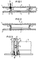
- the assembly shown schematically consists of two circuit boards 1 and 2 arranged in parallel which, as indicated by dash-dotted lines, are equipped on both sides, in particular with components using SMD technology.
- the electrical connection between the printed circuits of the circuit boards 1 and 2 is by means of a multi-pin connector, for. B. according to DIN 41612, which consists of two connector parts 3 (male connector) and 4 (female connector).
- the rectangular housing of the connector parts 3 and 4 are provided in a known manner on their narrow sides with mounting flanges 5 which have through holes 6.
- the one plug part 3 is fastened to the circuit board 1 by soldering its connecting pins, not shown here, to the printed circuit board.
- the through holes 7 provided in the printed circuit board 1 for carrying out retaining screws for the plug part 3 are left free.
- the other connector part 4 carries on its mounting flanges 5 spacers 8, which are provided with an internal thread 9. They are arranged coaxially to the through holes 6 in the mounting flanges 5 of the connector parts 3 and 4, so that a retaining screw 10 can be screwed from below through the printed circuit board 2 and the mounting flange 5 into the internal thread 9 of the spacer bolt 8, whereby the connector part 4 in is attached in the usual way.
- a screw 11 or 11 ' can be screwed in, the screw head of which has a hexagon socket 12 as an engagement for a screwdriver 13.
- the length L of the spacer bolts 8 is such that it corresponds approximately to the distance a between the mounting flanges 5 of the assembled connector parts 3 and 4 minus the screw head height h of the screws 11, 11 '.
- the diameter of the screw head of the screws 11, 11 ' is larger than the diameter of the through holes 7 in the upper circuit board 1.
- the outer surface of the spacer bolt 8 can be cylindrical or polygonal, preferably hexagonal. In the latter case, the spacer bolt can be inserted with its foot end into a recess provided as standard for accommodating hexagon nuts in the fastening flanges 5.
Landscapes
- Engineering & Computer Science (AREA)
- Microelectronics & Electronic Packaging (AREA)
- Coupling Device And Connection With Printed Circuit (AREA)
- Structures For Mounting Electric Components On Printed Circuit Boards (AREA)
Description
- Die Erfindung betrifft eine Vorrichtung zum Trennen zweier in Sandwich-Bauweise mittels vielpoliger Steckverbinder miteinander verbundener Leiterplatten gemäß Oberbegriff des Anspruchs 1.
- Insbesondere bei beidseitig bestückten Leiterplatten, die zu zweien oder mehreren parallel in Sandwich-Bauweise angeordnet sind, werden Steckverbindungen benötigt, die aus Platzgründen nicht wie üblich am Rande der Leiterplatten angeordnet werden können, sondern sich in zentralen Bereichen befinden. Das Zusammenfügen der Steckverbindung läßt sich ohne weiteres durch Aufdrücken der oberen Leiterplatte auf eine untere bewerkstelligen. Schwierig wird jedoch das Trennen der Steckverbinder, da gerade bei vielpoligen Steckverbindern eine erhebliche Abzugskraft erforderlich ist, die, läßt man sie auf die Ränder der Leiterplatten wirken, zum Verbiegen derselben und eventuell zum Beschädigen oder Absprengen von Bestückungselementen, insbesondere von solchen in SMD-Technik führen kann.
- Es besteht deshalb die Aufgabe, eine Vorrichtung zu schaffen, bei der mit einfachen Mitteln eine Trennung vielpoliger Steckverbindungen zwischen zwei benachbart angeordneten Leiterplatten vorgenommen werden kann.
- Eine Lösung der Aufgabe wird in einer Vorrichtung gesehen, die die Merkmale des Anspruchs 1 aufweist. Vorteilhafte Weiterbildungen sind Gegenstände der Unteransprüche.
- Mit einfachen mechanischen Mitteln dieser Vorrichtung, nämlich durch Betätigen zweier Schrauben, lassen sich die erheblichen Abzugswiderstände einer vielpoligen Steckverbindung zwischen zwei Leiterplatten überwinden.
- Zur Erläuterung der Erfindung ist in den Figuren 1 bis 3 ein Ausführungsbeispiel dargestellt.
- Figur 1
- zeigt eine Sandwich-Baugruppe mit zwei Leiterplatten in zusammengestecktem Zustand,
- Figur 2
- dieselbe Baugruppe nach Lösung der Steckverbindung und
- Figur 3
- die Vorrichtung im einzelnen.
- Die schematisch dargestellte Baugruppe besteht aus zwei parallel angeordneten Leiterplatten 1 und 2, die, wie strichpunktiert angedeutet, beidseitig bestückt sind, insbesondere mit Bauelementen in SMD-Technik. Die elektrische Verbindung zwischen den gedruckten Schaltungen der Leiterplatten 1 und 2 wird mittels eines vielpoligen Steckverbinders, z. B. nach DIN 41612, hergestellt, welcher aus zwei Steckerteilen 3 (Messerleiste) und 4 (Federleiste) besteht. Die quaderförmigen Gehäuse der Steckerteile 3 und 4 sind in bekannter Weise an ihren Schmalseiten mit Befestigungsflanschen 5 versehen, die Durchgangslöcher 6 aufweisen.
- Das eine Steckerteil 3 ist durch das hier nicht dargestellte Verlöten seiner Anschlußstifte mit dem Leiterbild der Leiterplatte 1 auf dieser befestigt. Die in der Leiterplatte 1 zur Durchführung von Halteschrauben für das Steckerteil 3 vorgesehenen Durchgangsbohrungen 7 sind frei gelassen.
- Das andere Steckerteil 4 trägt auf seinen Befestigungsflanschen 5 Abstandsbolzen 8, die mit Innengewinde 9 versehen sind. Sie sind koaxial zu den Durchgangslöchern 6 in den Befestigungsflanschen 5 der Steckerteile 3 und 4 angeordnet, so daß von unten her eine Halteschraube 10 durch die Leiterplatte 2 und den Befestigungsflansch 5 in das Innengewinde 9 des Abstandsbolzens 8 eingeschraubt werden kann, womit das Steckerteil 4 in üblicher Weise befestigt ist.
- Vom oberen freien Ende der Abstandsbolzen 8 her ist jeweils eine Schraube 11 bzw. 11′ einschraubbar, deren Schraubenkopf ein Innensechskant 12 als Eingriff für einen Schraubendreher 13 aufweist.
- Die Länge L der Abstandsbolzen 8 ist so bemessen, daß sie etwa dem Abstand a zwischen den Befestigungsflanschen 5 der zusammengefügten Steckerteile 3 und 4 abzüglich der Schraubenkopfhöhe h der Schrauben 11, 11′ entspricht. Der Durchmesser des Schraubenkopfs der Schrauben 11, 11′ ist größer als der Durchmesser der Durchgangsbohrungen 7 in der oberen Leiterplatte 1. Die Mantelfläche des Abstandsbolzens 8 kann zylindrisch oder polygon, vorzugsweise sechseckig, sein. Im letzteren Fall läßt sich der Abstandsbolzen mit seinem Fußende in eine serienmäßig vorhandene Vertiefung zur Aufnahme von Sechskantmuttern in den Befestigungsflanschen 5 verdrehsicher einfügen.
- In Figur 1 sind die Steckerteile 3 und 4 zusammengesteckt, die Schrauben 11, 11′ sind voll in die Abstandsbolzen 8 eingedreht.
Um die Steckverbindung zu trennen, wird durch die Bohrung 7 in der Leiterplatte 1 und der koaxial dazu verlaufenden Öffnung 6 im Befestigungsflansch 5 ein Schraubendreher 13 in den Kopf der Schraube 11 eingeführt und dieselbe um etwa fünf bis neun Umdrehungen herausgedreht. Entsprechend wird auf der anderen Seite mit der Schraube 11′ verfahren, bis die Steckverbindung gelöst ist. Dieser Zustand ist in Figur 2 dargestellt. Die obere Leiterplatte 1 läßt sich ohne weiteres abziehen. Daraufhin werden die Schrauben 11 und 11′ wieder voll in die Abstandsbolzen 8 eingedreht, so daß nach Vornahme einer Reparatur oder Umbestückung die Leiterplatte 1 mit ihrem Steckerteil 3 leicht auf das Steckerteil 4 aufgesetzt und durch Zusammendrücken die Verbindung hergestellt werden kann.
Claims (3)
- Vorrichtung zum Trennen zweier in Sandwich-Bauweise mittels vielpoliger Steckverbinder miteinander verbundener, bestückter Leiterplatten, wobei die quaderförmigen Steckerteile mit an den Schmalseiten angeordneten Befestigungsflanschen mit Durchgangslöchern in Steckrichtung senkrecht zur Ebene der jeweiligen Leiterplatte auf dieser angebracht sind, dadurch gekennzeichnet, daß das eine Steckerteil (3) durch Verlötung seiner Anschlußstifte mit dem Leiterbild auf der ersten Leiterplatte (1) befestigt ist und in dieser Durchgangsbohrungen (7) koaxial zu den Durchgangslöchern (6) in den Befestigungsflanschen (5) angebracht sind,
und daß auf den Befestigungsflanschen (5) des anderen Steckerteils (4) koaxial zu den Durchgangslöchern (6) Abstandsbolzen (8) mit Innengewinde (9) angeordnet sind, in welche von unten her Halteschrauben (10) zur Befestigung des Steckerteils (4) auf der anderen Leiterplatte (2) und von dem oberen freien Ende her Schrauben (11, 11′) eindrehbar sind, deren Kopfdurchmesser größer ist als der Durchmesser der Durchgangslöcher (6) in den Befestigungsflanschen (5), wobei die Länge (L) der Abstandsbolzen (8) etwa dem Abstand a der Befestigungsflansche (5) der beiden zusammengesteckten Steckerteile (3 und 4) abzüglich der Schraubenkopfhöhe (h) der oberen Schrauben (11) entspricht. - Vorrichtung nach Anspruch 1, dadurch gekennzeichnet, daß die Mantelflächen der Abstandsbolzen (8) zylindrisch oder polygon sind.
- Vorrichtung nach Anspruch 1, dadurch gekennzeichnet, daß die Schraubenköpfe der oberen Schrauben (11) mit Innensechskant- oder ähnlichen Eingriffen (12) für Schraubendreher (13) versehen sind.
Applications Claiming Priority (2)
| Application Number | Priority Date | Filing Date | Title |
|---|---|---|---|
| DE9102565U | 1991-03-04 | ||
| DE9102565U DE9102565U1 (de) | 1991-03-04 | 1991-03-04 | Vorrichtung zum Trennen zweier in Sandwich-Bauweise mittels vielpoliger Steckverbinder miteinander verbundener Leiterplatten |
Publications (2)
| Publication Number | Publication Date |
|---|---|
| EP0502381A1 EP0502381A1 (de) | 1992-09-09 |
| EP0502381B1 true EP0502381B1 (de) | 1994-10-12 |
Family
ID=6864886
Family Applications (1)
| Application Number | Title | Priority Date | Filing Date |
|---|---|---|---|
| EP92102942A Expired - Lifetime EP0502381B1 (de) | 1991-03-04 | 1992-02-21 | Vorrichtung zum Trennen zweier in Sandwich-Bauweise mittels vielpoliger Steckverbinder miteinander verbundener Leiterplatten |
Country Status (4)
| Country | Link |
|---|---|
| EP (1) | EP0502381B1 (de) |
| AT (1) | ATE112925T1 (de) |
| DE (2) | DE9102565U1 (de) |
| ES (1) | ES2061290T3 (de) |
Families Citing this family (1)
| Publication number | Priority date | Publication date | Assignee | Title |
|---|---|---|---|---|
| DE102019000575B4 (de) | 2019-01-26 | 2024-02-01 | Diehl Aerospace Gmbh | Ausheben von Leiterkarten |
Family Cites Families (1)
| Publication number | Priority date | Publication date | Assignee | Title |
|---|---|---|---|---|
| DE3432102C2 (de) * | 1984-08-31 | 1987-04-23 | Siemens AG, 1000 Berlin und 8000 München | Vorrichtung zum Stecken und Ziehen von Flachbaugruppen |
-
1991
- 1991-03-04 DE DE9102565U patent/DE9102565U1/de not_active Expired - Lifetime
-
1992
- 1992-02-21 EP EP92102942A patent/EP0502381B1/de not_active Expired - Lifetime
- 1992-02-21 AT AT92102942T patent/ATE112925T1/de not_active IP Right Cessation
- 1992-02-21 ES ES92102942T patent/ES2061290T3/es not_active Expired - Fee Related
- 1992-02-21 DE DE59200609T patent/DE59200609D1/de not_active Expired - Fee Related
Also Published As
| Publication number | Publication date |
|---|---|
| EP0502381A1 (de) | 1992-09-09 |
| ATE112925T1 (de) | 1994-10-15 |
| DE9102565U1 (de) | 1991-05-23 |
| ES2061290T3 (es) | 1994-12-01 |
| DE59200609D1 (de) | 1994-11-17 |
Similar Documents
| Publication | Publication Date | Title |
|---|---|---|
| DE69722055T2 (de) | Elektrischer Verbinder | |
| DE3909263C3 (de) | Elektrische Verbindungsvorrichtung | |
| DE19756345A1 (de) | Anordnung zur Kontaktierung von Leiterplatten | |
| DE69410426T2 (de) | Mehrfachverbinderanordnung | |
| DE3618470A1 (de) | Steckerkupplung | |
| DE4437316C2 (de) | Dezentrale Ein/Ausgabebaugruppe für elektronische Steuerungen | |
| EP0349878A1 (de) | Elektronik-Baugruppe | |
| DE102009047555A1 (de) | Elektrischer Steckverbinder niedriger Bauhöhe | |
| EP0397057A1 (de) | Anordnung zur mechanischen und elektrischen Verbindung einer Ergänzungsleiterplatte an einer Grundleiterplatte | |
| DE60204745T2 (de) | Verbindungseinrichtung zwischen Leiterplatten | |
| EP0098361B1 (de) | Relaisfassung | |
| DE102015224595B4 (de) | Gedruckte Leiterplatten-Einheit mit verbesserten Anschlüssen sowie Verfahren zu deren Herstellung | |
| DE4433735A1 (de) | Verschwenkbarer Verbinder für planare elektronische Vorrichtungen | |
| DE60118687T2 (de) | Verbinder zur Befestigung auf eine Leiterplatte und Anordnung zur Befestigung eines Verbinders auf eine Leiterplatte | |
| DE4226172C2 (de) | Stromversorgungselement für Leiterplatten | |
| DE29600371U1 (de) | Hochstrom-Kabelklemme für eine Leiterplattenanordnung | |
| EP0502381A1 (de) | Vorrichtung zum Trennen zweier in Sandwich-Bauweise mittels vielpoliger Steckverbinder miteinander verbundener Leiterplatten | |
| DE10105621B4 (de) | Elektrische Leiterplatte | |
| DE102005016760B4 (de) | Anordnung elektrischer bzw. elektronischer Geräte | |
| WO2000028627A1 (de) | Elektrisches leiterplatten-bauteil und verfahren zur automatischen bestückung von leiterplatten mit solchen bauteilen | |
| DE29614725U1 (de) | Steckeinrichtung | |
| DE3432102C2 (de) | Vorrichtung zum Stecken und Ziehen von Flachbaugruppen | |
| WO2022189046A1 (de) | Steckervorrichtung zum befestigen von elektronischen komponenten auf einer leiterplatte | |
| DE60201537T2 (de) | Elektrische verbindungsanordnung für elektronische bauteile | |
| EP2037469A1 (de) | Leiterplattenrelais |
Legal Events
| Date | Code | Title | Description |
|---|---|---|---|
| PUAI | Public reference made under article 153(3) epc to a published international application that has entered the european phase |
Free format text: ORIGINAL CODE: 0009012 |
|
| AK | Designated contracting states |
Kind code of ref document: A1 Designated state(s): AT BE CH DE ES FR GB IT LI NL SE |
|
| 17P | Request for examination filed |
Effective date: 19930204 |
|
| 17Q | First examination report despatched |
Effective date: 19940211 |
|
| GRAA | (expected) grant |
Free format text: ORIGINAL CODE: 0009210 |
|
| AK | Designated contracting states |
Kind code of ref document: B1 Designated state(s): AT BE CH DE ES FR GB IT LI NL SE |
|
| REF | Corresponds to: |
Ref document number: 112925 Country of ref document: AT Date of ref document: 19941015 Kind code of ref document: T |
|
| REF | Corresponds to: |
Ref document number: 59200609 Country of ref document: DE Date of ref document: 19941117 |
|
| REG | Reference to a national code |
Ref country code: ES Ref legal event code: FG2A Ref document number: 2061290 Country of ref document: ES Kind code of ref document: T3 |
|
| ITF | It: translation for a ep patent filed | ||
| GBT | Gb: translation of ep patent filed (gb section 77(6)(a)/1977) |
Effective date: 19941223 |
|
| EAL | Se: european patent in force in sweden |
Ref document number: 92102942.7 |
|
| ET | Fr: translation filed | ||
| PLBE | No opposition filed within time limit |
Free format text: ORIGINAL CODE: 0009261 |
|
| STAA | Information on the status of an ep patent application or granted ep patent |
Free format text: STATUS: NO OPPOSITION FILED WITHIN TIME LIMIT |
|
| 26N | No opposition filed | ||
| PGFP | Annual fee paid to national office [announced via postgrant information from national office to epo] |
Ref country code: GB Payment date: 19970123 Year of fee payment: 6 |
|
| PGFP | Annual fee paid to national office [announced via postgrant information from national office to epo] |
Ref country code: AT Payment date: 19970129 Year of fee payment: 6 |
|
| PGFP | Annual fee paid to national office [announced via postgrant information from national office to epo] |
Ref country code: SE Payment date: 19970213 Year of fee payment: 6 Ref country code: ES Payment date: 19970213 Year of fee payment: 6 |
|
| PGFP | Annual fee paid to national office [announced via postgrant information from national office to epo] |
Ref country code: BE Payment date: 19970221 Year of fee payment: 6 |
|
| PGFP | Annual fee paid to national office [announced via postgrant information from national office to epo] |
Ref country code: NL Payment date: 19970225 Year of fee payment: 6 Ref country code: FR Payment date: 19970225 Year of fee payment: 6 |
|
| PGFP | Annual fee paid to national office [announced via postgrant information from national office to epo] |
Ref country code: DE Payment date: 19970418 Year of fee payment: 6 |
|
| PGFP | Annual fee paid to national office [announced via postgrant information from national office to epo] |
Ref country code: CH Payment date: 19970522 Year of fee payment: 6 |
|
| PG25 | Lapsed in a contracting state [announced via postgrant information from national office to epo] |
Ref country code: GB Free format text: LAPSE BECAUSE OF NON-PAYMENT OF DUE FEES Effective date: 19980221 Ref country code: AT Free format text: LAPSE BECAUSE OF NON-PAYMENT OF DUE FEES Effective date: 19980221 |
|
| PG25 | Lapsed in a contracting state [announced via postgrant information from national office to epo] |
Ref country code: SE Free format text: LAPSE BECAUSE OF NON-PAYMENT OF DUE FEES Effective date: 19980222 |
|
| PG25 | Lapsed in a contracting state [announced via postgrant information from national office to epo] |
Ref country code: ES Free format text: LAPSE BECAUSE OF NON-PAYMENT OF DUE FEES Effective date: 19980223 |
|
| PG25 | Lapsed in a contracting state [announced via postgrant information from national office to epo] |
Ref country code: LI Free format text: LAPSE BECAUSE OF NON-PAYMENT OF DUE FEES Effective date: 19980228 Ref country code: FR Free format text: THE PATENT HAS BEEN ANNULLED BY A DECISION OF A NATIONAL AUTHORITY Effective date: 19980228 Ref country code: CH Free format text: LAPSE BECAUSE OF NON-PAYMENT OF DUE FEES Effective date: 19980228 Ref country code: BE Free format text: LAPSE BECAUSE OF NON-PAYMENT OF DUE FEES Effective date: 19980228 |
|
| BERE | Be: lapsed |
Owner name: SIEMENS A.G. Effective date: 19980228 |
|
| PG25 | Lapsed in a contracting state [announced via postgrant information from national office to epo] |
Ref country code: NL Free format text: LAPSE BECAUSE OF NON-PAYMENT OF DUE FEES Effective date: 19980901 |
|
| GBPC | Gb: european patent ceased through non-payment of renewal fee |
Effective date: 19980221 |
|
| REG | Reference to a national code |
Ref country code: CH Ref legal event code: PL |
|
| EUG | Se: european patent has lapsed |
Ref document number: 92102942.7 |
|
| NLV4 | Nl: lapsed or anulled due to non-payment of the annual fee |
Effective date: 19980901 |
|
| PG25 | Lapsed in a contracting state [announced via postgrant information from national office to epo] |
Ref country code: DE Free format text: LAPSE BECAUSE OF NON-PAYMENT OF DUE FEES Effective date: 19981103 |
|
| REG | Reference to a national code |
Ref country code: FR Ref legal event code: ST |
|
| REG | Reference to a national code |
Ref country code: ES Ref legal event code: FD2A Effective date: 20000403 |
|
| PG25 | Lapsed in a contracting state [announced via postgrant information from national office to epo] |
Ref country code: IT Free format text: LAPSE BECAUSE OF NON-PAYMENT OF DUE FEES;WARNING: LAPSES OF ITALIAN PATENTS WITH EFFECTIVE DATE BEFORE 2007 MAY HAVE OCCURRED AT ANY TIME BEFORE 2007. THE CORRECT EFFECTIVE DATE MAY BE DIFFERENT FROM THE ONE RECORDED. Effective date: 20050221 |