EP0500915B1 - Method of configuring a memory system - Google Patents
Method of configuring a memory system Download PDFInfo
- Publication number
- EP0500915B1 EP0500915B1 EP91918179A EP91918179A EP0500915B1 EP 0500915 B1 EP0500915 B1 EP 0500915B1 EP 91918179 A EP91918179 A EP 91918179A EP 91918179 A EP91918179 A EP 91918179A EP 0500915 B1 EP0500915 B1 EP 0500915B1
- Authority
- EP
- European Patent Office
- Prior art keywords
- memory
- bank
- dram devices
- populated
- size
- Prior art date
- Legal status (The legal status is an assumption and is not a legal conclusion. Google has not performed a legal analysis and makes no representation as to the accuracy of the status listed.)
- Expired - Lifetime
Links
Images


Classifications
-
- G—PHYSICS
- G06—COMPUTING OR CALCULATING; COUNTING
- G06F—ELECTRIC DIGITAL DATA PROCESSING
- G06F12/00—Accessing, addressing or allocating within memory systems or architectures
- G06F12/02—Addressing or allocation; Relocation
- G06F12/06—Addressing a physical block of locations, e.g. base addressing, module addressing, memory dedication
- G06F12/0607—Interleaved addressing
-
- G—PHYSICS
- G06—COMPUTING OR CALCULATING; COUNTING
- G06F—ELECTRIC DIGITAL DATA PROCESSING
- G06F12/00—Accessing, addressing or allocating within memory systems or architectures
- G06F12/02—Addressing or allocation; Relocation
- G06F12/06—Addressing a physical block of locations, e.g. base addressing, module addressing, memory dedication
- G06F12/0646—Configuration or reconfiguration
- G06F12/0684—Configuration or reconfiguration with feedback, e.g. presence or absence of unit detected by addressing, overflow detection
Definitions
- This invention relates to the field of multiple bank dynamic random access memory (DRAM) systems and in particular to a method for identifying bank memory size.
- DRAM dynamic random access memory
- a computer system consists of a number of modules or components.
- Computer systems typically include a central processing unit (CPU) such as a microprocessor.
- the microprocessor is a program-controlled device that obtains, decodes and executes instructions.
- a computer system also includes program storage components for storing program instructions, and data storage components for storing data. These storage components may be read only memory (ROM), random access memory (RAM), disc or tape storage, or any other suitable storage means.
- a computer system also includes input/output (I/O) components for connecting external devices to the microprocessor.
- I/O input/output
- Special purpose components such as memory management units or co-processors may also be part of the computer system.
- Main memory is a scarce resource that is dynamically allocated to users, programs, or processes.
- Main memory is typically a silicon based memory such as a random access memory (RAM).
- RAM random access memory
- DRAM dynamic random access memory
- DRAM dynamic random access memory
- the clock rate of operation of the microprocessor has increased. This increases the memory access time requirements of the main memory associated with the microprocessor.
- the access time of DRAM has not kept pace with the requirements of present microprocessor technology. For example, 16 and 32 bit microprocessors may require memory access rates of 20 to 40 nanoseconds. Present day DRAM has access times of 60 to 80 nanoseconds. To satisfy the access requirements of present-day microprocessors, memory caching schemes or page access schemes are utilized.
- SRAM static RAM
- bank switching One memory scheme used to achieve high performance without the cost, task switching or conversion penalties of caching schemes is known as "bank switching". This scheme utilizes a number of banks of DRAM and interleaves access to the DRAMs to "hide” the precharge time of individual banks.
- One such scheme is described in U. S. patent application number 604,785 entitled “METHOD AND APPARATUS FOR PAGE PREDICTION OF MULTIPLE PAGE DRAM", filed on October 26, 1990, assigned to the assignee of the present invention and published as EP 482 575 A.
- US 4908789 A discloses a method and system for configuring a memory system using modules of different capacities, based on size information provided as a code by the modules.
- IBM Technical Disclosure Bulletin Vol. 29, No. 3, August 1986, page 1381 'Memory presence detect' describes the detection of module presence by reading an address bus which may have certain pins tied to a fixed voltage level to indicate empty/full memory sockets.
- a method by which a memory controller determines memory size in an interleaved multiple bank DRAM memory system is described.
- the method ensures that an associated CPU can access a contiguous memory array.
- the offset to the next bank is identified with the memory size.
- a memory controller that is capable of controlling a given size DRAM identifies memory below a maximum size by asserting a high or low level on the most significant address pins. By reading the address pins as input, the controller can determine that memory space is not available on the higher address locations and the offset for the next bank can be determined.
- a method for memory size identification for configuring a multiple bank DRAM memory system is described.
- numerous specific details such as number of bits, number of memory banks, etc. are set forth in detail in order to provide a more thorough description of the invention. It will be apparent, however, to one skilled in the art, that the present invention may be practiced without these specific details. In other instances, well-known features have not been described in detail so as not to unnecessarily obscure the present invention.
- a microprocessor or central processing unit is a device for obtaining, decoding and executing instructions.
- a microprocessor requires an associated memory to hold information. This memory is referred to as "main memory” and is used to hold instruction sequences (programs) and to store data.
- main memory is used to hold instruction sequences (programs) and to store data.
- the speed of a memory depends on the "access time”, "write time', and "memory cycle time”.
- the "access time” of a memory corresponds to the time required to provide a read control signal to the memory and apply the address bits to memory, until the output of the memory is valid.
- “Write time” is the time between the sending of a write signal to memory and when new data has been written to the memory.
- Memory cycle time is the time period required to complete a specific memory function, such as a read/write operation, a read/read operation, a write/write operation, or a write/read operation.
- Main memory in a computer system has a logical organization and a physical organization.
- the physical organization of the main memory of a computer system typically consists of a memory array coupled to a computer system bus for communication with a microprocessor and other computer system components. Each address location in the main memory is accessed by a "physical address".
- the physical main memory location in which informational items may be stored is called the physical address space or the physical memory space.
- logical address An address used by or generated by a program to specify a particular informational item is called a "logical address.”
- the set of logical addresses used by a program to identity informational items is called the "logical address space.”
- the logical organization of a memory must include a mapping means for converting a logical address space to a physical address space. (It should be noted that the logical address space need not be equal to the physical address space.)
- a virtual memory scheme In many applications, it is desired to provide a greater logical address space than the physical address space of main memory. This is accomplished through a technique known as "virtual memory.” In a virtual memory scheme, the logical address space is represented in the physical main memory and in secondary mass storage such as hard disk drives or floppy disk drives. A virtual memory scheme requires a mechanism to determine whether an addressed element resides in physical memory or in secondary mass storage. When an addressed item does not reside in physical memory, it must be transferred from secondary storage in a process known as "swapping".
- a memory paging scheme permits main memory to be allocated in small blocks of equal size called "page frames".
- a "page” (set of contiguous logical addresses) fits within a page frame. Paging permits the implementation of a logical address space larger than the installed physical memory. If a reference page is missing from a physical memory, it is swapped in from secondary storage as a single unit; that is, the entire page is swapped into physical memory.
- DRAM physical memory
- the maximum memory size that is addressable by a memory controller depends on the number of pins available. If a memory size less than the maximum is used, certain of the pins (the most significant address bits) are not used. Separate and additional I/O pins are provided for software control of memory selection, adding to device complexity and expense.
- the present invention is a method for configuring an interleaved multiple bank DRAM memory system as defined in claim 1.
- An interleaving scheme can provide improved operation if the memory accesses are sequential.
- the interleave scheme is used to "hide" the precharge time of the DRAM's (which affects access time) for sequential addressing.
- a block diagram of the environment of the present invention is illustrated in Figure 1.
- a microprocessor or CPU 10 includes an address bus 14, control bus 15 and data bus 16.
- the address bus 14 is coupled to a DRAM controller 17.
- the memory controller 17 permits the definition of various size memory arrays without the need for additional I/O lines.
- the DRAM controller communicates on buses 19A-19D with DRAM memory banks 20A -20D, respectively.
- the control bus 15 and data bus 16 are coupled to a decoder 18 which provides output on bus 22.
- the DRAM memory banks communicate with an auxiliary memory on bus 21.
- the four memory banks are driven by four independent channels 19A-19D.
- the memory array is between 1 and 256 megabytes in the present embodiment but can be any suitable size.
- Each DRAM can be 256 k bit, 1 megabit, 4 megabit or 16 megabit. While one of the memory banks is accessed, the three remaining banks are loaded in advance in order to avoid wait states when the program advances from the current bank or page.
- the memory banks are interleaved so that the physical addresses on any given page of memory are stacked above each other.
- An example of the memory organization of the DRAM memory banks is as follows. In this example, a 256k x 4 DRAM having a 9 bit wide row address equivalent to 512 pages is utilized:
- a high hit rate is accomplished by mapping the address space in contiguous banks so that a linearly progressing program will access distinguished pages. Therefore, a page change will not result in a wait state for precharging the memory.
- FIG. 2 A memory configuration which may be used with the present invention is illustrated in Figure 2.
- the memories are divided into four separate arrays of 9 memories each, identified as bank A through D.
- Bank A contains memories 30A-38A;
- Bank B contains memories 30B-38B;
- Bank C includes memories 30C-38C, and
- Bank D includes memories 30D-38D.
- Each memory can be 64 kilobits by 4, 256 kilobits by 4 or one megabyte x 4.
- Memories 38A-38D receive parity bits for data validation.
- Row address select signals RASA-RASD are provided to memory banks A-D respectively, to select a row in the memory array. Column select signals then select the appropriate column so the desired memory element may be read.
- column select signals CASA 0-CASA 3 are provided.
- CASA 0 is coupled to memory banks 36A and 37A.
- Signal CASA 1 is coupled to banks 34A and 35A.
- Signal CASA 2 is coupled to banks 32A and 33A.
- Signal CASA 3 is coupled to banks 30A and 31A.
- column select signals CAS B0 - B3 are provided to the memories of bank B; signal CAS C0-C3 are provided to bank C, and signal CAS D0-D3 are provided to bank D.
- the DRAM controller 17 is coupled to the processor control bus 15.
- the processor control bus 15 provides control signals to control block 43.
- the signals include W/R, D/C. M/O, Reset, ADS, Clock, RS16, and A20 gate signals.
- the processor address bus 14 provides address information to address latch 44.
- the control block 43 provides output signal 46 to delay line block 68 and signal 47 to the RAS/CAS generator block 69.
- the delay line block 68 provides output signal 70 to the RAS/CAS generator block 69.
- a byte enable signal 40 provided by a microprocessor is also coupled to the control block 17 and is provided as signal 48 to the RAS/CAS generator block 69.
- the address latch 44 provides output 45 to a page replacement block 53, logic block 55 and program flow detector block 59.
- Mode select signals 41 are provided to mode control block 49.
- Mode control block 49 provides an output 50 to RAS/CAS generator block 69.
- a disable refresh signal 42 is provided to refresh block 51.
- Refresh block 51 includes a counter so that appropriate rows and columns can be refreshed as desired.
- the refresh block 51 provides an output signal 52 to the RAS/CAS generator block 69.
- the RAS/CAS generator block 69 is also coupled on line 54 to replacement block 53.
- the page replacement block 53 includes an up/down counter and provides outputs 56, 57, and 58 to logic block 55.
- the program flow detector block 59 provides an output signal 72 to flag block 60.
- Flag block 60 provides an increment/decrement signal 61 to page replacement block 53.
- Logic block 55 provides output signal 71 to the up/down counter of page replacement block 53.
- the RAS/CAS generator block 69 provides output 62 to output blocks 64A, 64B, 64C and 64D.
- the page replacement block 53 provides output on bus 65 to output blocks 64A-64D, respectively.
- the output blocks 64A-64D provide address information on Q busses 19A-19D respectively, to memory banks A through D.
- the output blocks 64A-64D also provide the row address signals, column address signals CAS 0-CAS 3 for each of the memory banks and a write enable signal.
- Each Q bus for example, is 12 bits wide and can address a maximum of 16 megabits in a memory bank. If a memory bank is resized to a smaller size than the maximum, then certain of the Q lines are not used.
- the present invention provides a method for using these unused address lines to convey memory sizing information to the controller.
- the memory depth used with the embodiments of this invention is selectable for each individual bank from 16K to 16 megabits.
- the memory of banks B, C and D is mapped to contiguous boundaries to achieve a linear address space for improved operation. Size selection is accomplished by connecting unused Q outputs to VCC or VSS. After power up or reset, the controller asserts a current on the five highest order Q outputs (Q7-Q11). By reading the input, the controller can determine the memory size and the offset for each bank The offset is a function of the memory depth and is equal to memory size multiplied by memory width. This is a cost effective way to provide various memory sizes and to allow upgrades without having to replace existing memory devices.
- Q6 is tied to VSS.
- Q7-Q11 can be left open.
- the banks populate in sequential order and may not have a gap in between.
- the memory organization can be by eight, by four and by one.
- banks 64A-64D each have 12 bit Q lines 19A-19D, respectively.
- bank A a 16 megabit bank, all 12 address lines are used.
- bank B only 10 bits are used because only 1 megabit of memory is addressed. The unused address bits are used to provide information about the memory mapping. Lines Q10-Q11 of bank B are tied to VSS. Only the address lines Q0-Q9 of bank B are utilized.
- address line Q6 is tied to VSS. This embodiment utilizes this convention to indicate that the bank is not populated. Any single one of the the Q lines can be set to VSS to indicate this state, or any combination of Q lines can be utilized without departing from the scope of this invention. Alternatively, each line Q0-Q11 can be coupled to VSS to indicate that the bank is unpopulated.
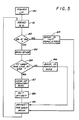
- the memory controller executes an algorithm on power-up to determine the memory size of the DRAM banks. This algorithm is illustrated in the flow diagram of Figure 5.
- the DRAM and DRAM controller are powered up.
- the DRAM controller reads line Q6 of the first memory bank, bank A.
- step 82 the argument "Is Q6 at VSS?" is made. If the argument at decision block is true, the system proceeds to step 83 and the memory controller identifies block A as not populated. If the argument at decision block 82 is false, the system proceeds to step 84. At step 84, the address lines Q7-Q11 are polled.
- the argument "Is at least one line of lines Q7-Q11 at VSS?" is made. If the argument at decision block 85 is false, (i.e. none of the lines Q7-Q11 are at VSS), the system proceeds to step 86 and the bank is identified as being of maximum size.
- step 87 the memory of the memory block is determined by identifying which Q lines are at VSS and referring to a table to locate memory size.
- step 88 the offset for the memory is determined based on the memory size.
- Steps 83, 86 and 88 all proceed to step 89.
- step 89 the process is repeated for each memory bank.
- the memory size and offset for each memory bank is determined by referring to Table 1 below: Q lines at VSS Memory Size Offset Q11 4 Meg 4 Meg x Memory Width Q11, Q10 1 Meg 1 Meg x Memory Width Q11, Q10, Q9 256K 256K x Memory Width Q11, Q10, Q9, Q8 64K 64K x Memory Width Q11, Q10, Q9, Q8, Q7 16K 16K x Memory Width
Landscapes
- Engineering & Computer Science (AREA)
- Theoretical Computer Science (AREA)
- Physics & Mathematics (AREA)
- General Engineering & Computer Science (AREA)
- General Physics & Mathematics (AREA)
- Dram (AREA)
Applications Claiming Priority (3)
| Application Number | Priority Date | Filing Date | Title |
|---|---|---|---|
| US58328390A | 1990-09-17 | 1990-09-17 | |
| US583283 | 1990-09-17 | ||
| PCT/US1991/006714 WO1992005491A1 (en) | 1990-09-17 | 1991-09-17 | Method and apparatus for memory size selection |
Publications (3)
| Publication Number | Publication Date |
|---|---|
| EP0500915A1 EP0500915A1 (en) | 1992-09-02 |
| EP0500915A4 EP0500915A4 (enExample) | 1994-01-12 |
| EP0500915B1 true EP0500915B1 (en) | 2000-02-02 |
Family
ID=24332459
Family Applications (1)
| Application Number | Title | Priority Date | Filing Date |
|---|---|---|---|
| EP91918179A Expired - Lifetime EP0500915B1 (en) | 1990-09-17 | 1991-09-17 | Method of configuring a memory system |
Country Status (4)
| Country | Link |
|---|---|
| EP (1) | EP0500915B1 (enExample) |
| AU (1) | AU8722691A (enExample) |
| DE (1) | DE69131958T2 (enExample) |
| WO (1) | WO1992005491A1 (enExample) |
Families Citing this family (1)
| Publication number | Priority date | Publication date | Assignee | Title |
|---|---|---|---|---|
| CN121478671B (zh) * | 2025-10-30 | 2026-08-04 | 算苗科技(北京)有限公司 | 一种存储器模组及其数据处理方法 |
Family Cites Families (10)
| Publication number | Priority date | Publication date | Assignee | Title |
|---|---|---|---|---|
| US4234934A (en) * | 1978-11-30 | 1980-11-18 | Sperry Rand Corporation | Apparatus for scaling memory addresses |
| FR2443735A1 (fr) * | 1978-12-06 | 1980-07-04 | Cii Honeywell Bull | Dispositif de controle automatique de la capacite memoire mise en oeuvre dans les systemes de traitements de l'information |
| JPS55110355A (en) * | 1979-02-16 | 1980-08-25 | Toshiba Corp | Memory board and selection system for it |
| GB2087607B (en) * | 1980-11-06 | 1984-10-24 | British Gas Corp | Computer-based control system |
| US4566082A (en) * | 1983-03-23 | 1986-01-21 | Tektronix, Inc. | Memory pack addressing system |
| JPS62190999U (enExample) * | 1986-05-23 | 1987-12-04 | ||
| US4908789A (en) * | 1987-04-01 | 1990-03-13 | International Business Machines Corporation | Method and system for automatically assigning memory modules of different predetermined capacities to contiguous segments of a linear address range |
| US4951248A (en) * | 1988-03-04 | 1990-08-21 | Sun Microsystems, Inc. | Self configuring memory system |
| US5027313A (en) * | 1988-08-25 | 1991-06-25 | Compaq Computer Corporation | Apparatus for determining maximum usable memory size |
| US5012408A (en) * | 1990-03-15 | 1991-04-30 | Digital Equipment Corporation | Memory array addressing system for computer systems with multiple memory arrays |
-
1991
- 1991-09-17 DE DE69131958T patent/DE69131958T2/de not_active Expired - Lifetime
- 1991-09-17 WO PCT/US1991/006714 patent/WO1992005491A1/en not_active Ceased
- 1991-09-17 AU AU87226/91A patent/AU8722691A/en not_active Abandoned
- 1991-09-17 EP EP91918179A patent/EP0500915B1/en not_active Expired - Lifetime
Also Published As
| Publication number | Publication date |
|---|---|
| WO1992005491A1 (en) | 1992-04-02 |
| EP0500915A1 (en) | 1992-09-02 |
| DE69131958T2 (de) | 2000-10-12 |
| DE69131958D1 (de) | 2000-03-09 |
| EP0500915A4 (enExample) | 1994-01-12 |
| AU8722691A (en) | 1992-04-15 |
Similar Documents
| Publication | Publication Date | Title |
|---|---|---|
| JP3590413B2 (ja) | メモリ制御装置 | |
| US4860252A (en) | Self-adaptive computer memory address allocation system | |
| KR100265263B1 (ko) | 프로그램가능 공용 메모리 시스템 및 방법 | |
| CA2116985C (en) | Memory system | |
| US5761732A (en) | Interleaving for memory cards | |
| US4601018A (en) | Banked memory circuit | |
| JP2000090005A (ja) | バンク・ビット割り当て方法 | |
| US6041016A (en) | Optimizing page size in mixed memory array using address multiplexing | |
| KR100822617B1 (ko) | 컴퓨터 시스템 | |
| US5572692A (en) | Memory configuration decoding system having automatic row base address generation mechanism for variable memory devices with row access interleaving | |
| US6505282B1 (en) | Method and apparatus for determining memory types of a multi-type memory subsystem where memory of the different types are accessed using column control signals with different timing characteristics | |
| US6535966B1 (en) | System and method for using a page tracking buffer to reduce main memory latency in a computer system | |
| AU648259B2 (en) | Centralized reference and change table for a multiprocessor virtual memory system | |
| US20060095694A1 (en) | Method of memory space configuration | |
| US5367655A (en) | Memory and associated method including an operating mode for simultaneously selecting multiple rows of cells | |
| US6571323B2 (en) | Memory-access management method and system for synchronous dynamic Random-Access memory or the like | |
| HK1003851B (en) | A memory apparatus and method for use in a data processing system | |
| US6906978B2 (en) | Flexible integrated memory | |
| US6430648B1 (en) | Arranging address space to access multiple memory banks | |
| US6542958B1 (en) | Software control of DRAM refresh to reduce power consumption in a data processing system | |
| US7787311B2 (en) | Memory with programmable address strides for accessing and precharging during the same access cycle | |
| US5630098A (en) | System and method for interleaving memory addresses between memory banks based on the capacity of the memory banks | |
| US20040042320A1 (en) | Address decode | |
| EP0500915A4 (enExample) | ||
| US6433786B1 (en) | Memory architecture for video graphics environment |
Legal Events
| Date | Code | Title | Description |
|---|---|---|---|
| PUAI | Public reference made under article 153(3) epc to a published international application that has entered the european phase |
Free format text: ORIGINAL CODE: 0009012 |
|
| 17P | Request for examination filed |
Effective date: 19920604 |
|
| AK | Designated contracting states |
Kind code of ref document: A1 Designated state(s): DE FR GB IT |
|
| RIN1 | Information on inventor provided before grant (corrected) |
Inventor name: SPONRING, OTTO |
|
| A4 | Supplementary search report drawn up and despatched |
Effective date: 19930809 |
|
| AK | Designated contracting states |
Kind code of ref document: A4 Designated state(s): DE FR GB IT |
|
| 17Q | First examination report despatched |
Effective date: 19981012 |
|
| GRAG | Despatch of communication of intention to grant |
Free format text: ORIGINAL CODE: EPIDOS AGRA |
|
| RIC1 | Information provided on ipc code assigned before grant |
Free format text: 6G 06F 12/06 A |
|
| RTI1 | Title (correction) |
Free format text: METHOD OF CONFIGURING A MEMORY SYSTEM |
|
| GRAG | Despatch of communication of intention to grant |
Free format text: ORIGINAL CODE: EPIDOS AGRA |
|
| GRAH | Despatch of communication of intention to grant a patent |
Free format text: ORIGINAL CODE: EPIDOS IGRA |
|
| GRAH | Despatch of communication of intention to grant a patent |
Free format text: ORIGINAL CODE: EPIDOS IGRA |
|
| GRAA | (expected) grant |
Free format text: ORIGINAL CODE: 0009210 |
|
| AK | Designated contracting states |
Kind code of ref document: B1 Designated state(s): DE FR GB IT |
|
| PG25 | Lapsed in a contracting state [announced via postgrant information from national office to epo] |
Ref country code: IT Free format text: LAPSE BECAUSE OF FAILURE TO SUBMIT A TRANSLATION OF THE DESCRIPTION OR TO PAY THE FEE WITHIN THE PRE;WARNING: LAPSES OF ITALIAN PATENTS WITH EFFECTIVE DATE BEFORE 2007 MAY HAVE OCCURRED AT ANY TIME BEFORE 2007. THE CORRECT EFFECTIVE DATE MAY BE DIFFERENT FROM THE ONE RECORDED.SCRIBED TIME-LIMIT Effective date: 20000202 |
|
| REF | Corresponds to: |
Ref document number: 69131958 Country of ref document: DE Date of ref document: 20000309 |
|
| ET | Fr: translation filed | ||
| PLBE | No opposition filed within time limit |
Free format text: ORIGINAL CODE: 0009261 |
|
| STAA | Information on the status of an ep patent application or granted ep patent |
Free format text: STATUS: NO OPPOSITION FILED WITHIN TIME LIMIT |
|
| 26N | No opposition filed | ||
| REG | Reference to a national code |
Ref country code: GB Ref legal event code: IF02 |
|
| PGFP | Annual fee paid to national office [announced via postgrant information from national office to epo] |
Ref country code: GB Payment date: 20100826 Year of fee payment: 20 |
|
| PGFP | Annual fee paid to national office [announced via postgrant information from national office to epo] |
Ref country code: FR Payment date: 20101018 Year of fee payment: 20 |
|
| PGFP | Annual fee paid to national office [announced via postgrant information from national office to epo] |
Ref country code: DE Payment date: 20100909 Year of fee payment: 20 |
|
| REG | Reference to a national code |
Ref country code: DE Ref legal event code: R071 Ref document number: 69131958 Country of ref document: DE |
|
| REG | Reference to a national code |
Ref country code: DE Ref legal event code: R071 Ref document number: 69131958 Country of ref document: DE |
|
| REG | Reference to a national code |
Ref country code: GB Ref legal event code: PE20 Expiry date: 20110916 |
|
| PG25 | Lapsed in a contracting state [announced via postgrant information from national office to epo] |
Ref country code: GB Free format text: LAPSE BECAUSE OF EXPIRATION OF PROTECTION Effective date: 20110916 |
|
| PG25 | Lapsed in a contracting state [announced via postgrant information from national office to epo] |
Ref country code: DE Free format text: LAPSE BECAUSE OF EXPIRATION OF PROTECTION Effective date: 20110918 |