EP0500481B1 - Schaltung und Verfahren zur Auswahl der k-grössten Daten einer Datenfolge - Google Patents
Schaltung und Verfahren zur Auswahl der k-grössten Daten einer Datenfolge Download PDFInfo
- Publication number
- EP0500481B1 EP0500481B1 EP92420054A EP92420054A EP0500481B1 EP 0500481 B1 EP0500481 B1 EP 0500481B1 EP 92420054 A EP92420054 A EP 92420054A EP 92420054 A EP92420054 A EP 92420054A EP 0500481 B1 EP0500481 B1 EP 0500481B1
- Authority
- EP
- European Patent Office
- Prior art keywords
- data
- datum
- output
- modules
- bit
- Prior art date
- Legal status (The legal status is an assumption and is not a legal conclusion. Google has not performed a legal analysis and makes no representation as to the accuracy of the status listed.)
- Expired - Lifetime
Links
Images


Classifications
-
- G—PHYSICS
- G06—COMPUTING; CALCULATING OR COUNTING
- G06F—ELECTRIC DIGITAL DATA PROCESSING
- G06F9/00—Arrangements for program control, e.g. control units
- G06F9/06—Arrangements for program control, e.g. control units using stored programs, i.e. using an internal store of processing equipment to receive or retain programs
- G06F9/30—Arrangements for executing machine instructions, e.g. instruction decode
- G06F9/30003—Arrangements for executing specific machine instructions
- G06F9/30007—Arrangements for executing specific machine instructions to perform operations on data operands
- G06F9/30021—Compare instructions, e.g. Greater-Than, Equal-To, MINMAX
-
- G—PHYSICS
- G06—COMPUTING; CALCULATING OR COUNTING
- G06F—ELECTRIC DIGITAL DATA PROCESSING
- G06F7/00—Methods or arrangements for processing data by operating upon the order or content of the data handled
- G06F7/22—Arrangements for sorting or merging computer data on continuous record carriers, e.g. tape, drum, disc
-
- Y—GENERAL TAGGING OF NEW TECHNOLOGICAL DEVELOPMENTS; GENERAL TAGGING OF CROSS-SECTIONAL TECHNOLOGIES SPANNING OVER SEVERAL SECTIONS OF THE IPC; TECHNICAL SUBJECTS COVERED BY FORMER USPC CROSS-REFERENCE ART COLLECTIONS [XRACs] AND DIGESTS
- Y10—TECHNICAL SUBJECTS COVERED BY FORMER USPC
- Y10S—TECHNICAL SUBJECTS COVERED BY FORMER USPC CROSS-REFERENCE ART COLLECTIONS [XRACs] AND DIGESTS
- Y10S707/00—Data processing: database and file management or data structures
- Y10S707/99931—Database or file accessing
- Y10S707/99937—Sorting
Definitions
- the present invention relates to sorting circuits of data according to a determined criterion and in particular a circuit allowing to select the k largest data of a sequence of data arriving sequentially.
- sorting circuits are for example useful in the frame of image compression.
- a first technique of the prior art for providing the largest coefficients of the transformed matrix is to read the coefficients sequentially and compare them to a threshold value to cancel those below the threshold.
- This technique has the disadvantage of canceling all the coefficients a matrix if they are all small; this results in a significant degradation of the reconstructed image because the most large of these small coefficients correspond to information significant. It also has the disadvantage of do not cancel any of the coefficients if they are all greater than threshold and the compression target is not reached.
- a second technique consists in keeping only one determined number k of the largest data. So, we are sure not to cancel small values which are still representative of the image and not having to process more than k data in a later step. So far the circuits of implementation of this second technique have the drawback to be complex and relatively slow.
- the present invention provides a method using works this second technique in a particularly way simple.
- the present invention provides a method of selecting the k data of greatest value in a series of n data arriving sequentially in the form of binary logic signals, comprising the following steps: a) sequentially writing each of the data in one of n memories adapted to each receive a word comprising, in order of decreasing bit weights: a first inhibit bit, a second selection bit, third bits of the data, fourth bits corresponding to a number representative of rank d 'arrival of the data; b) set the first bits of the n words to 1 when the first of the signals corresponding to the data sequence arrives; c) when writing each of the data, zero the first and second bits of the corresponding word; d) between the arrivals of the signals corresponding to the (nk) th datum and to the n th datum, detect the smallest of the words contained in the memories and set its second bit to 1; and e) as soon as the signals corresponding to the n th datum arrive, read the stored data sequentially and process differently those whose word has the
- step e) the data is read in the order of their writing in step a).
- the present invention also provides a circuit for selecting the k data of greatest value in a series of n data presented sequentially on an input bus in the form of binary logic signals, comprising: a matrix of memory points of n columns and m rows , each column being assigned to a word corresponding to one of the data and comprising in order of increasing row numbers and decreasing bit weights: a first inhibition memory point set to one by an initialization signal and set to zero by the arrival of the data, a second selection memory point connected to a line of an output bus, set to zero by the arrival of the data, third memory points connected to the lines of the bus data input and a data output bus, for receiving and storing the data, and fourth memory points containing a number representative of the rank of arrival of the data; a first circuit for addressing each of the columns at the rate of arrival of the data and writing there the data present on the lines of the input bus; a second active circuit only between the arrival of the (nk) th datum and the arrival of the n th datum to detect the word of
- the second circuit consists of modules, each one being associated with a memory point and comprising: a connection to the output Q of the associated memory point, an exclusion output X ij , which, if the current row i is the last, is connected to a setting input to 1 of the second memory point of the current column j, an intermediate output, a linked exclusion input, or else to the exclusion output X i-1 , j of the module of the current column j and of the previous row i-1, or else to 0 if the current row is the first, a detection input connected to the output Z i of a logic detection means common to all the modules of the current row j and receiving as input the intermediate outputs of these modules; the output X ij taking the values summarized in the following table where the symbol "#" designates either 0 or 1: Z i X i-1, j X ij # 1 1 0 0 0 1 0 Q the intermediate output taking the value 1 if
- the logic detection means supplies the value 0 at its output Z i only when all the intermediate outputs of the modules of the current row j are at 1.
- the circuits for addressing each of the columns are made up a shift register.
- the second memory points are authorized to be set to 1 by an active validation signal between the arrivals of the (nk) th data and of the n th data.
- An advantage of the present invention is that the selection k larger data is complete upon arrival of the last data of the continuation, whereas in the prior art one was forced to sort and sort the data in descending order into a memory and then take the first k.
- any element affected by the index j corresponds to the j th data item in the sequence.
- each word D j is associated in binary with a word comprising additional bits, namely, in decreasing order of bit weight, an inhibition bit I j , a selection bit S j , the bits of the data D j , and priority bits P j .
- the bits P j represent in binary a priority coefficient equal to nj (here 8-j).
- Each of the words is placed in a memory, for example according to a column.
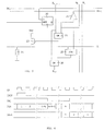
- the contents of the memory are illustrated under form of a table represented in FIGS. 1A to 1P at different filling stages, the first row representing the bit states I, the second bit state S, the third the decimal values of the D data and the fourth the values decimals of priority coefficients P.
- FIG. 1A represents the state of this table as soon as the first data D 1 of a series of eight data arrives.
- the "#" symbol represents any value.
- the bits I of the 8 columns are set to 1.
- the first column is selected for writing, a column selected for writing being indicated by the letter W at the top of the column.
- the data D 1 is written there and at the same time the bits I 1 and S 1 are set to zero.
- the fifth datum D 5 is written in the table in the same way in the fifth column.
- the smallest word is detected in the 8 columns, a detection being represented by a framed column. It is necessarily one of the words of the first 5 columns since their first bits I are at 0 while the first I bits of the words in the other columns are at 1.
- the selection bit S 1 is set to 1 as soon as the next data item D 6 arrives in FIG. 1F.
- the setting to 1 is represented by a framed 1. Due to the setting of the bit S 1 of the word in the first column (the smallest), this becomes the largest of the five which have just been written and can no longer be selected as the smallest during following comparisons.
- the data D 6 to D 8 are written during the steps illustrated in FIGS. 1F to 1H in the same way in columns 6 to 8. It is successively detected that the words in columns 6, 5 and 8 are the smallest and we set to 1 their bits S 6 , S 5 and S 8 .
- FIG. 1H at the same time as writing the data D 8 , the sequence for reading the data begins.
- each of the data is read in the order of their arrival with the corresponding bit S.
- a column selected for reading is indicated by the letter R at the top of the column.
- the bit S marks by 0 the four largest data and by 1 the others. It is then possible, for example in the context of an application to image compression, to cancel the data marked with 1.
- a drawback may result from the fact that the first datum D 1 is the last datum marked by setting the bit S 1 to 1 .
- Figure 1H we will read the data D 1 with its bit S 1 which has not yet been set to 1, because this bit is set to 1 at the next time in Figure 1I.
- this case never arises because the first data are the largest, in particular when this circuit processes data coming from a cosine transform.
- a solution to this drawback will be proposed in FIG. 5.
- This process is easily generalizable to select the k largest data in a sequence of n data. Instead of having eight words and columns, we will have n and the selection of the k smallest of these n words is active after the arrival of the (nk) th data. After the arrival of the n th data, the selection is inactive and we will have marked the nk smallest columns by setting their 1 bits to 1. Thus, there remain k columns marked with a 0 in their corresponding S bits, which indicates that the k largest data are written there. During n following times, the n data are read with their S bits and it is possible to cancel those marked with a 1 in the S bits.
- FIG. 2 represents a particular embodiment of a circuit implementing the method described above.
- This circuit includes a matrix of modules for storing and processing a bit.
- this matrix will include n columns, like those in the tables in FIGS. 1A to 1B.
- this matrix comprises m rows, the number m corresponding to the number of bits of a column of the tables previously described.
- the first row includes MI modules (MI 11 ... MI 1j ... MI 1n ) for the inhibition bits I.
- the second row includes MS modules (MS 21 ... MS 2j ... MS 2n ) intended for selection bits S.
- the following r rows include MD modules (MD 31 ... MD 3j ... MD 3n to MD 2 + r, 1 . .. MD 2 + r, j ... MD 2 + r, n ).
- the last p rows include MP priority modules (MP 3 + r, 1 ... MP 3 + r, j ... MP 3 + r, n to MP m1 ... MP mj ... MP mn ) intended to contain in binary form the priority words designated by the letter P in the tables of FIGS. 1A to 1P (p represents the number of bits necessary for coding the numbers 0 to n-1).
- i is a row index.
- Each of the modules includes a bit input (except the MP modules), a bit output (except the MI and MP modules), an exclusion input, an exclusion output X ij , a read authorization input (except MP modules) and a write authorization input (except MP modules).
- the MI and MS modules additionally include a SET entry for setting 1.
- the MP modules binary code the priority coefficients in a fixed manner.
- the bit input is connected to an IN line i of an input bus
- the bit output is connected to an OUT line i of an output bus
- the output Xj exclusion ij is connected to the module's exclusion input of the next row i + 1.
- All the modules of a row i are also connected to a common line Z i whose role will be understood during the explanation of FIG. 3.
- the write authorization input is linked to a line W j of a write address bus and the read authorization input is linked to a line R j of a read address bus.
- the first reading line R 1 is connected to the last writing line W n , which will cause the first column to be read and the last to be written simultaneously.
- the lines W and R are controlled by an addressing circuit 11 of conventional constitution, consisting for example of a shift register, controlled by a clock CK and by an initialization signal INIT also applied to the first writing line W 1 .
- the bit inputs of the first two rows are connected to logic level 0 (ground).
- the exclusion inputs of the modules MI are connected to logic level 0.
- the exclusion output X mj of each of the modules MP mj of the last row is connected to the input D of a flip-flop 10.
- Each of the flip-flops 10 is of type D and has a reverse output Q * connected to the SET input for setting the MS module to 1 in the corresponding column, a validation entry linked to a CK clock and a SET input set to 1 connected to a line VAL validation common to all scales 10.
- each MI, MS, MD and MP module of a column corresponds in particular at a memory point suitable for memorizing a bit of the word contained in the corresponding column of the tables of FIGS. 1A to 1P.
- Each of the MI, MS, MD and MP modules includes, in addition to the memory point, a logical processing unit which, in combination with that of all the other modules, performs the operations previously explained, namely comparison operations values of the words stored in the columns and column selection operations. (This selection operation consisting in setting the selection bit S of the module MS of each columns).
- this circuit must take into account some additional logical combinations, namely that no exclusion bit must be emitted in the case where, for all the columns not previously excluded, all the modules of the same row contain a 1 (for example above the MD 42 , MD 43 and MD 45 modules then the MD 62 and MD 65 modules then the MP 85 module and finally the MP 95 module).
- Figure 3 shows one of the modules in the form of a logic diagram.
- a memory point consisting of a flip-flop 20 of type D comprises a bit input D connected to one of the lines In i ; a validation input linked to one of the writing lines W j ; an output Q connected to one of the lines OUT i via a three-state gate 21 activated by its control input connected to one of the read lines R j ; and a SET input for setting in the case of the MI and MS modules.
- the MP modules do not have a flip-flop and the wires which would correspond to the outputs of the flip-flops are connected either to ground (0 logic) or to the supply voltage Vcc (1 logic) to form the coefficients of priority nj in binary.
- An OR (OR) gate 22 receives the output Q of the flip-flop 20 and the exclusion output X i-1, j of the module of the previous line.
- the output of the OR gate 22 feeds the gate of a P-channel MOS transistor 23 whose source is connected to the supply voltage Vcc and whose drain is connected to the line Z i .
- a resistive means 24 (only one per line) connects the line Z i to the ground.
- the set of MOS transistors 23 of the same row and the resistive means 24 constitute a NAND gate. This NAND gate has the line Z i as an output and each of its inputs is connected to the outputs of the OR gates of the same row.
- NAND gate a zero detector which provides at its output a 1 when at least one of its inputs is at 0.
- An AND (AND) gate 25 is connected as an input to the output Q of flip-flop 20 and at line Z i .
- An OR (OR) gate 26 receives the output of AND gate 25 and the exclusion output X i-1, j of the previous module. the output of the OR gate 26 constitutes the exclusion output X ij .
- a module works as follows.
- This 1 is present on one of the inputs of OR gate 26 and is transmitted to the output of this gate, which constitutes the exclusion output X ij.
- each module satisfies the function of direct transmission of an exclusion bit produced by an earlier module of the same column.
- Line Z i is forced to 1 by any of the modules of the same row whose MOS transistor 23 is conductive, that is to say whose OR gate 22 has its output at 0. This only occurs if the exclusion entry and the contents of the flip-flop are at 0, which means that the column to which the module in question belongs necessarily contains one of the smallest words.
- the line Z i is forced to 0 by the resistive means 24 only if all the MOS transistors 23 of the modules of the same row are blocked. This occurs when each of the modules in the row has its exclusion entry at 1 or the contents of its flip-flop 20 at 1. This occurs in the case where all the modules in the row and in non-excluded columns contain a 1 in their flip-flop 20. In this case, all the outputs of AND gates 25 of the modules in the row are at 0 and this 0 is transmitted to the exclusion outputs of all the modules of the row located in non-excluded columns.
- the three columns respectively represent the values taken by the line Z i , the exclusion output of the module of the previous row i-1 and of the same column j, and the exclusion output X ij of the module considered.
- the symbol "#" represents either 0 or 1 and Q indicates the content of flip-flop 20 of the module considered.
- each module performs the following write and read operations.
- a 1 present on line W j which is connected to the validation input of flip-flop 20 makes it possible to load into the flip-flop the bit present at this time there on line IN i connected to bit input D of flip-flop .
- a 1 present on the reading line R j which is connected to the control input of the three-state gate 21 allows the transmission of the content Q of the flip-flop on the line OUT i connected to the output of the three-state gate 21.
- FIG. 4 represents a timing diagram where CK designates the clock signal; INIT the initialization signal applied to line W 1 and at the input of the addressing circuit 11; VAL the validation signal applied to the validation line; Din the instants of appearance of each of the data D j on the lines IN i of the input bus; and Dout the instants of appearance of each of the data D j at the output of the circuit on the lines OUT i of the output bus.
- the signal INIT is at 0 and the signal VAL is at 1, the signals Din and Dout are arbitrary.
- the signal INIT goes high for a clock period, authorizing the writing of the data item D 1 in the modules MD of the first column. ; the flip-flops of the MI modules of the first row are set to 1 and the addressing circuit 11 is initialized.
- the addressing circuit presents a 1 on line W 2 during a clock period, which authorizes the writing of the data D 2 in the modules MD of the second column and so on until the writing of the n data successively in each of the MD i1 to MD in module sets.
- all the modules in the matrix begin to calculate the column containing the smallest word and a 0 appears at the exclusion output of the last module in this column.
- the flip-flops 10 are active, that is to say that their outputs Q * are no longer forced to 0 by the signal VAL and that they take into account the bits present on their inputs; in particular at the next rising edge of the clock (as of the arrival of the following data), the flip-flop 10 of the column containing the smallest word transmits at its output Q * a 1 putting the module MS corresponding to 1.
- the addressing circuit 11 authorizes the transfer of the first data D 1 as well as of the selection bit S 1 stored respectively in the modules MD 31 to MD 2 + r1 and MS 1 on the data output bus, and so on until the MD and MS modules in the last column are read.
- FIG. 5 illustrates a simple modification of the circuit of the present invention, making it possible to overcome the drawback previously mentioned according to which, when the first datum D 1 is the last marked datum, the marking bit S 1 of this datum D 1 n ' is not yet forced to 1 while this marking bit and the data D 1 are read.
- FIG. 5 partially shows the circuit of a modified MS 21 module, the last MP module m1 and the flip-flop 10 for setting the MS 21 module to 1.
- the comparison begins and, shortly after, an exclusion bit X m1 equal to 0 will appear at the output of the module MP m1 indicating that the datum D 1 must be marked.
- the marking flip-flop 20 is set to 1 only at the next rising edge of the clock CK when the exclusion bit X m1 is transferred to the inverted output Q * of flip-flop 10.
- the reading line R 1 is set to 1 and the gate 21 transmits on the line OUT 2 the output of the OR gate 50.
- the flip-flop 20 is not yet at 1, the output of the OR gate 50 , and therefore the line OUT 2 , will be set to 1 when the bit X m1 will be set to 0.
- the marking bit S 1 presented on the line OUT 2 is established a certain time after the establishment of the bits of the data D 1 on the other lines OUT, but, as in general these bits are taken into account by the circuit which uses them at the next falling edge of the clock CK, this delay, being less than the half-period of clock, will not cause error.
- a circuit easy to carry out by a person skilled in the art can be placed after the circuit of figure 2 to cancel the data marked with a 1 in their selection bits S correspondents.
- circuit of the embodiment of the invention described in connection with Figure 2 is a circuit of the systolic type where each of the modules constitutes a systole. This kind of circuit is easy to integrate because its routing is simplified.
- T Z + (m-1) T M designates the duration of selection of the smallest of the n columns.
- T Z designates the time for establishing a bit on a line Z
- m designates the number of modules in a column
- T M designates the computation time of a module. This duration is particularly short.
- the invention has been described in the context of a treatment image, but it applies wherever you need select the k largest or smallest data in a dataset.
- the logic circuit shown in Figure 3 is given to as an example. Of course, we can get the same functions with a large number of different logic circuits. The functions of these circuits can also be performed with a suitably programmed microprocessor associated with memories.
- MP priority modules have been described as having fixed content, but it can just as easily be editable like the content of other modules, to obtain variable priority orders.
Landscapes
- Engineering & Computer Science (AREA)
- Theoretical Computer Science (AREA)
- General Engineering & Computer Science (AREA)
- Physics & Mathematics (AREA)
- General Physics & Mathematics (AREA)
- Software Systems (AREA)
- Computer Hardware Design (AREA)
- Image Processing (AREA)
- Compression Or Coding Systems Of Tv Signals (AREA)
- Logic Circuits (AREA)
- Compression, Expansion, Code Conversion, And Decoders (AREA)
- Communication Control (AREA)
Claims (7)
- Verfahren zum Auswählen der k Daten von größtem Betrag in einer Folge von sequentiell in Form binärer Digitalsignale ankommenden n Daten,
dadurch gekennzeichnet, daß das Verfahren die folgenden Schritte umfaßt:a) jedes der Daten wird sequentiell in einen von n Speichern eingeschrieben, deren jeder jeweils ein Datenwort aufnehmen kann, welches in der Reihenfolge abnehmender Bit-Wertigkeit enthält:ein erstes Inhibitions- bzw. Sperr-Bit (Ij),ein zweites Selektions-Bit (Sj),dritte Daten-Bits (Dj) des betreffenden Datums,vierte Bits (P), welche einer den Eintreffrang des Datums wiedergebenden Zahl entsprechen,b) beim Eintreffen des ersten der der Datenfolge entsprechenden Signale werden die ersten Bits (Ij) der n Datenworte (auf Eins) gesetzt,c) beim Einschreiben jedes der Daten (Dj) werden die ersten (Ij) und die zweiten (Sj) Bits des entsprechenden Datenworts (auf Null) rückgestellt,d) zwischen dem Ankommen der dem (n-k)-ten Datum und dem n-ten Datum entsprechenden Signale wird das in den Speichern enthaltene kleinste Datenwort festgestellt und sein zweites Bit (Sj) (auf Eins) gesetzt, sowiee) beim Eintreffen der dem n-ten Datum entsprechenden Signale werden sequentiell die gespeicherten Daten gelesen und diejenigen, in deren Datenwort das zweite Bit (Sj) Eins beträgt, in anderer Weise behandelt als diejenigen, bei denen dieses Bit den Wert Null besitzt. - Verfahren nach Anspruch 1,
dadurch gekennzeichnet, daß in der Verfahrensstufe e) die Daten in der Reihenfolge ihres Einschreibens in der Verfahrensstufe a) gelesen werden. - Schaltung zum Auswählen der k Daten mit dem größten Betrag in einer Folge von n Daten, die sequentiell auf einem Eingangs-Bus in Form binärer Digitalsignale ankommen, dadurch gekennzeichnet, daß die Schaltung umfaßt:eine Punktspeichermatrix (20) mit n Spalten und m Zeilen, wobei jeweils jede Spalte einem einem der Daten entsprechenden Datenwort zugewiesen ist und in der Reihenfolge zunehmender Zeilenzahlen und abnehmender Bit-Wertigkeiten umfaßt:einen ersten Inhibitions- bzw. Sperr-Speicherpunkt (MI), der durch ein Initialisiersignal (INIT) auf Eins gesetzt und beim Ankommen des Datums auf Null rückgestellt wird,einen zweiten Selektions-Speicherpunkt (MS), der mit einer Leitung eines Ausgangs-Bus verbunden ist und beim Ankommen des Datums auf Null gestellt wird,dritte Speicherpunkte (MD), welche mit den Leitungen des Dateneingangs-Bus und den Leitungen eines Datenausgangs-Bus verbunden sind, zum Empfang und zum Speichern des Datums, sowievierte Speicherpunkte (MP), welche eine den Eintreffrang des Datums wiedergebende Zahl enthalten,eine erste Schaltung zur Adressierung jeder der Spalten im Rhythmus des Eintreffens der Daten und zum Einschreiben des jeweils auf den Leitungen des Eingangs-Bus anliegenden Datums in die Kolonne,eine zweite Schaltung, die nur zwischen dem Ankommen des (n-k)-ten Datums und dem Ankommen des n-ten Datums aktiv ist, um das Wort mit dem kleinsten Betrag festzustellen und seinen zweiten Speicherpunkt beim Eintreffen des nächsten Datums auf Eins zu setzen, sowieeine dritte Schaltung zum Adressieren jeder der Spalten im Rhythmus des Eintreffens der Daten und zum Einschreiben der Bits, die in den zweiten und dritten Speicherpunkten auf den Leitungen des Ausgangsdaten-Bus beim Schreiben des n-ten Datums enthalten sind.
- Schaltung nach Anspruch 3,
dadurch gekennzeichnet, daß die zweite Schaltung aus Modulen besteht, deren jeder jeweils einem Speicherpunkt zugeordnet ist und umfaßt:wobei der Ausgang (Xij) die in der folgenden Tabelle zusammengestellten Werte annimmt, wobei das Symbol "#" indifferent 0 oder 1 bedeutet:eine Verbindung mit dem Q-Ausgang des zugehörigen Speicherpunktes,einen Exklusionsausgang (Xjj), der, wenn die laufende Zeile (i) die letzte (m) ist, mit einem Setz-Eingang des zweiten Speicherpunkts der laufenden Spalte (j) verbunden wird,einen Zwischenausgang,einen Exklusionsausgang, der entweder mit dem Exklusionsausgang (Xi-1,j) des Moduls der laufenden Spalte (j) und der vorhergehenden Zeile (i-j), oder mit "0" verbunden ist, wenn die laufende Zeile die erste ist,einen Detektionseingang, der mit dem Ausgang (Zi) einer sämtlichen Modulen der laufenden Zeile (j) gemeinsamen Nachweis- oder Detektionslogik (23, 24) verbunden ist, welche am Eingang die Zwischenausgänge dieser Module zugeführt erhält,Zi Xi-1,j Xij # 1 1 0 0 0 1 0 Q - Schaltung nach Anspruch 4,
dadurch gekennzeichnet, daß die Detektionslogikschaltung an ihrem Ausgang (Zi) den Wert 0 nur liefert, wenn sämtliche Zwischenausgänge der Module der laufenden Zeile (j) den Wert "1" besitzen. - Schaltung nach Anspruch 3,
dadurch gekennzeichnet, daß die Schaltungen zur Adressierung jeder der Spalten durch ein Schieberegister gebildet werden. - Schaltung nach Anspruch 3,
dadurch gekennzeichnet, daß die zweiten Speicherpunkte zwischen dem Eintreffen des (n-k)-ten Datums und des n-ten Datums durch ein aktives Validier- bzw. Betätigungssignal zur Stellung auf Eins autorisiert werden.
Applications Claiming Priority (2)
| Application Number | Priority Date | Filing Date | Title |
|---|---|---|---|
| FR9102301 | 1991-02-21 | ||
| FR9102301A FR2673301B1 (fr) | 1991-02-21 | 1991-02-21 | Circuit et procede de selection des k plus grandes donnees d'une suite de donnees. |
Publications (2)
| Publication Number | Publication Date |
|---|---|
| EP0500481A1 EP0500481A1 (de) | 1992-08-26 |
| EP0500481B1 true EP0500481B1 (de) | 1998-04-29 |
Family
ID=9410121
Family Applications (1)
| Application Number | Title | Priority Date | Filing Date |
|---|---|---|---|
| EP92420054A Expired - Lifetime EP0500481B1 (de) | 1991-02-21 | 1992-02-19 | Schaltung und Verfahren zur Auswahl der k-grössten Daten einer Datenfolge |
Country Status (5)
| Country | Link |
|---|---|
| US (1) | US5421010A (de) |
| EP (1) | EP0500481B1 (de) |
| JP (1) | JP3218669B2 (de) |
| DE (1) | DE69225260T2 (de) |
| FR (1) | FR2673301B1 (de) |
Families Citing this family (1)
| Publication number | Priority date | Publication date | Assignee | Title |
|---|---|---|---|---|
| EP0984355A3 (de) * | 1998-09-01 | 2002-06-05 | Siemens Aktiengesellschaft | Vorrichtung zur schnellen Bestimmung n grösster Signale, wobei n eine vorgebbare Anzahl ist |
Family Cites Families (3)
| Publication number | Priority date | Publication date | Assignee | Title |
|---|---|---|---|---|
| JPS55116101A (en) * | 1979-03-01 | 1980-09-06 | Nissan Motor Co Ltd | Signal processor |
| FR2607641B1 (fr) * | 1986-12-02 | 1989-02-10 | Efcis | Filtre numerique de rang k et procede de filtrage correspondant |
| JPH0310486A (ja) * | 1989-06-07 | 1991-01-18 | Matsushita Electric Ind Co Ltd | 動画像符号化装置 |
-
1991
- 1991-02-21 FR FR9102301A patent/FR2673301B1/fr not_active Expired - Fee Related
-
1992
- 1992-02-19 DE DE69225260T patent/DE69225260T2/de not_active Expired - Fee Related
- 1992-02-19 EP EP92420054A patent/EP0500481B1/de not_active Expired - Lifetime
- 1992-02-21 JP JP06997492A patent/JP3218669B2/ja not_active Expired - Fee Related
-
1994
- 1994-06-28 US US08/267,293 patent/US5421010A/en not_active Expired - Lifetime
Also Published As
| Publication number | Publication date |
|---|---|
| JPH05150945A (ja) | 1993-06-18 |
| EP0500481A1 (de) | 1992-08-26 |
| FR2673301A1 (fr) | 1992-08-28 |
| DE69225260T2 (de) | 1998-11-19 |
| JP3218669B2 (ja) | 2001-10-15 |
| FR2673301B1 (fr) | 1994-02-18 |
| US5421010A (en) | 1995-05-30 |
| DE69225260D1 (de) | 1998-06-04 |
Similar Documents
| Publication | Publication Date | Title |
|---|---|---|
| EP0198729B1 (de) | System zur Simulation einer elektronischen Schaltung | |
| EP0322966B1 (de) | Neuronale Netzwerkschaltung und -struktur | |
| FR2686990A1 (fr) | Unite arithmetique ayant une operation d'accumulation. | |
| FR2629248A1 (fr) | Procede de test de memoire a programmation unique et memoire correspondante | |
| EP0485921B1 (de) | Vorrichtung für die Verarbeitung des Viterbi-Algorithmus mit einem Prozessor und einer spezialisierten Einheit | |
| FR2588142A1 (fr) | Systeme permettant le traitement a haute vitesse par convolutions de donnees d'image. | |
| FR2650694A1 (fr) | Memoire vive pour machine de traitement de donnees | |
| EP0298002A1 (de) | Transpositionsspeicher für eine Datenverarbeitungsschaltung | |
| EP0166838A1 (de) | Verfahren und Anordnung zur Detektion einer besonderen Bitkonfiguration in einem seriellen Bitstrom | |
| EP0519847B1 (de) | Speicherkarte zur Zählung von Daten und Lesevorrichtung | |
| EP0863512B1 (de) | Doppelzugriffspeicher | |
| EP0500481B1 (de) | Schaltung und Verfahren zur Auswahl der k-grössten Daten einer Datenfolge | |
| FR2586312A1 (fr) | Dispositif d'autocorrelation | |
| EP0833346B1 (de) | Serieller Zugriffsspeicher mit Schreibsicherung | |
| EP1772808B1 (de) | Vorrichtung und Verfahren zum Lesen von Daten in einer Ansammlung von elektronischen Bauteilen, die mit einem Kommunikationsbus verbunden sind, angewendet auf das Lesen einer Matrix von Pixeln | |
| FR2475250A1 (fr) | Multiplieur rapide | |
| FR2741977A1 (fr) | Appareil pour la transformation d'un cosinus discret bidimensionnel | |
| EP1642388B1 (de) | Einrichtung zum vergleichen zweier wörter von jeweils n bit | |
| US11487990B2 (en) | Resistive crossbar arrays with reduced numbers of elements | |
| EP1542233A1 (de) | Serieller Speicher mit Mitteln zum Schutz eines erweiterten Speicherfeldes während einer Schreiboperation | |
| EP0432008A1 (de) | Elektronisches Neuronalnetzwerk und Lernverfahren | |
| EP0266267A1 (de) | Sequentielles Adressierverfahren eines Speichers | |
| EP0375054A1 (de) | Künstliche neuronale integrierte Schaltung mit Lernmitteln | |
| EP0640910A1 (de) | Verfahren zur Steuerung einer FIFO-Schaltung und Einrichtung zu seiner Durchführung | |
| EP4354351A1 (de) | Elektronische schaltung auf rram-zellenbasis |
Legal Events
| Date | Code | Title | Description |
|---|---|---|---|
| PUAI | Public reference made under article 153(3) epc to a published international application that has entered the european phase |
Free format text: ORIGINAL CODE: 0009012 |
|
| AK | Designated contracting states |
Kind code of ref document: A1 Designated state(s): DE FR GB IT |
|
| 17P | Request for examination filed |
Effective date: 19930125 |
|
| GRAG | Despatch of communication of intention to grant |
Free format text: ORIGINAL CODE: EPIDOS AGRA |
|
| 17Q | First examination report despatched |
Effective date: 19970901 |
|
| GRAG | Despatch of communication of intention to grant |
Free format text: ORIGINAL CODE: EPIDOS AGRA |
|
| GRAH | Despatch of communication of intention to grant a patent |
Free format text: ORIGINAL CODE: EPIDOS IGRA |
|
| GRAH | Despatch of communication of intention to grant a patent |
Free format text: ORIGINAL CODE: EPIDOS IGRA |
|
| GRAA | (expected) grant |
Free format text: ORIGINAL CODE: 0009210 |
|
| AK | Designated contracting states |
Kind code of ref document: B1 Designated state(s): DE FR GB IT |
|
| ITF | It: translation for a ep patent filed |
Owner name: MITTLER & C. S.R.L. |
|
| GBT | Gb: translation of ep patent filed (gb section 77(6)(a)/1977) |
Effective date: 19980506 |
|
| REF | Corresponds to: |
Ref document number: 69225260 Country of ref document: DE Date of ref document: 19980604 |
|
| RAP4 | Party data changed (patent owner data changed or rights of a patent transferred) |
Owner name: STMICROELECTRONICS S.A. |
|
| PLBE | No opposition filed within time limit |
Free format text: ORIGINAL CODE: 0009261 |
|
| STAA | Information on the status of an ep patent application or granted ep patent |
Free format text: STATUS: NO OPPOSITION FILED WITHIN TIME LIMIT |
|
| 26N | No opposition filed | ||
| REG | Reference to a national code |
Ref country code: GB Ref legal event code: IF02 |
|
| PGFP | Annual fee paid to national office [announced via postgrant information from national office to epo] |
Ref country code: DE Payment date: 20020306 Year of fee payment: 11 |
|
| PG25 | Lapsed in a contracting state [announced via postgrant information from national office to epo] |
Ref country code: DE Free format text: LAPSE BECAUSE OF NON-PAYMENT OF DUE FEES Effective date: 20030902 |
|
| PGFP | Annual fee paid to national office [announced via postgrant information from national office to epo] |
Ref country code: FR Payment date: 20040210 Year of fee payment: 13 |
|
| PGFP | Annual fee paid to national office [announced via postgrant information from national office to epo] |
Ref country code: GB Payment date: 20040218 Year of fee payment: 13 |
|
| PG25 | Lapsed in a contracting state [announced via postgrant information from national office to epo] |
Ref country code: IT Free format text: LAPSE BECAUSE OF NON-PAYMENT OF DUE FEES;WARNING: LAPSES OF ITALIAN PATENTS WITH EFFECTIVE DATE BEFORE 2007 MAY HAVE OCCURRED AT ANY TIME BEFORE 2007. THE CORRECT EFFECTIVE DATE MAY BE DIFFERENT FROM THE ONE RECORDED. Effective date: 20050219 Ref country code: GB Free format text: LAPSE BECAUSE OF NON-PAYMENT OF DUE FEES Effective date: 20050219 |
|
| GBPC | Gb: european patent ceased through non-payment of renewal fee |
Effective date: 20050219 |
|
| PG25 | Lapsed in a contracting state [announced via postgrant information from national office to epo] |
Ref country code: FR Free format text: LAPSE BECAUSE OF NON-PAYMENT OF DUE FEES Effective date: 20051031 |
|
| REG | Reference to a national code |
Ref country code: FR Ref legal event code: ST Effective date: 20051031 |