EP0496357A2 - Charge coupled device - Google Patents
Charge coupled device Download PDFInfo
- Publication number
- EP0496357A2 EP0496357A2 EP92100939A EP92100939A EP0496357A2 EP 0496357 A2 EP0496357 A2 EP 0496357A2 EP 92100939 A EP92100939 A EP 92100939A EP 92100939 A EP92100939 A EP 92100939A EP 0496357 A2 EP0496357 A2 EP 0496357A2
- Authority
- EP
- European Patent Office
- Prior art keywords
- charge transfer
- intermediate output
- transfer
- section
- gate electrode
- Prior art date
- Legal status (The legal status is an assumption and is not a legal conclusion. Google has not performed a legal analysis and makes no representation as to the accuracy of the status listed.)
- Granted
Links
- 239000012535 impurity Substances 0.000 claims abstract description 6
- 238000009792 diffusion process Methods 0.000 claims description 3
- 238000005036 potential barrier Methods 0.000 abstract description 12
- 239000004065 semiconductor Substances 0.000 abstract description 7
- 239000000758 substrate Substances 0.000 abstract description 7
- 230000006866 deterioration Effects 0.000 abstract 1
- VYPSYNLAJGMNEJ-UHFFFAOYSA-N Silicium dioxide Chemical compound O=[Si]=O VYPSYNLAJGMNEJ-UHFFFAOYSA-N 0.000 description 6
- 238000010586 diagram Methods 0.000 description 6
- 230000002542 deteriorative effect Effects 0.000 description 5
- XUIMIQQOPSSXEZ-UHFFFAOYSA-N Silicon Chemical compound [Si] XUIMIQQOPSSXEZ-UHFFFAOYSA-N 0.000 description 3
- 238000005070 sampling Methods 0.000 description 3
- 229910052710 silicon Inorganic materials 0.000 description 3
- 239000010703 silicon Substances 0.000 description 3
- 229910052681 coesite Inorganic materials 0.000 description 2
- 229910052906 cristobalite Inorganic materials 0.000 description 2
- 229910021420 polycrystalline silicon Inorganic materials 0.000 description 2
- 229920005591 polysilicon Polymers 0.000 description 2
- 239000000377 silicon dioxide Substances 0.000 description 2
- 235000012239 silicon dioxide Nutrition 0.000 description 2
- 229910052814 silicon oxide Inorganic materials 0.000 description 2
- 229910052682 stishovite Inorganic materials 0.000 description 2
- 229910052905 tridymite Inorganic materials 0.000 description 2
- 230000003111 delayed effect Effects 0.000 description 1
- 230000000694 effects Effects 0.000 description 1
- 238000012986 modification Methods 0.000 description 1
- 230000004048 modification Effects 0.000 description 1
Images


Classifications
-
- H—ELECTRICITY
- H01—ELECTRIC ELEMENTS
- H01L—SEMICONDUCTOR DEVICES NOT COVERED BY CLASS H10
- H01L27/00—Devices consisting of a plurality of semiconductor or other solid-state components formed in or on a common substrate
- H01L27/14—Devices consisting of a plurality of semiconductor or other solid-state components formed in or on a common substrate including semiconductor components sensitive to infrared radiation, light, electromagnetic radiation of shorter wavelength or corpuscular radiation and specially adapted either for the conversion of the energy of such radiation into electrical energy or for the control of electrical energy by such radiation
- H01L27/144—Devices controlled by radiation
- H01L27/146—Imager structures
- H01L27/148—Charge coupled imagers
-
- H—ELECTRICITY
- H01—ELECTRIC ELEMENTS
- H01L—SEMICONDUCTOR DEVICES NOT COVERED BY CLASS H10
- H01L29/00—Semiconductor devices specially adapted for rectifying, amplifying, oscillating or switching and having potential barriers; Capacitors or resistors having potential barriers, e.g. a PN-junction depletion layer or carrier concentration layer; Details of semiconductor bodies or of electrodes thereof ; Multistep manufacturing processes therefor
- H01L29/66—Types of semiconductor device ; Multistep manufacturing processes therefor
- H01L29/68—Types of semiconductor device ; Multistep manufacturing processes therefor controllable by only the electric current supplied, or only the electric potential applied, to an electrode which does not carry the current to be rectified, amplified or switched
- H01L29/76—Unipolar devices, e.g. field effect transistors
- H01L29/762—Charge transfer devices
- H01L29/765—Charge-coupled devices
- H01L29/768—Charge-coupled devices with field effect produced by an insulated gate
- H01L29/76833—Buried channel CCD
-
- H—ELECTRICITY
- H01—ELECTRIC ELEMENTS
- H01L—SEMICONDUCTOR DEVICES NOT COVERED BY CLASS H10
- H01L29/00—Semiconductor devices specially adapted for rectifying, amplifying, oscillating or switching and having potential barriers; Capacitors or resistors having potential barriers, e.g. a PN-junction depletion layer or carrier concentration layer; Details of semiconductor bodies or of electrodes thereof ; Multistep manufacturing processes therefor
- H01L29/66—Types of semiconductor device ; Multistep manufacturing processes therefor
- H01L29/68—Types of semiconductor device ; Multistep manufacturing processes therefor controllable by only the electric current supplied, or only the electric potential applied, to an electrode which does not carry the current to be rectified, amplified or switched
- H01L29/76—Unipolar devices, e.g. field effect transistors
- H01L29/762—Charge transfer devices
- H01L29/765—Charge-coupled devices
- H01L29/768—Charge-coupled devices with field effect produced by an insulated gate
- H01L29/76816—Output structures
Definitions
- the present invention generally relates to CCD (charge coupled device) delay lines and, more particularly, is directed to a CCD delay line which employs a floating gate (FG) or a floating diffusion gate at its intermediate output portion.
- CCD charge coupled device
- CCD delay lines are devices which make effective use of charge transfer and/or time operation function to delay or vary a signal from a timing standpoint, thereby processing a signal.
- the CCD delay line is different from a CCD image pickup element in that signal charges are calculated by an input signal voltage and injected while signal charges are generated and injected by the incidence of light according to the CCD image pickup element.
- Td becomes substantially equal to the horizontal synchronizing frequency of a television signal.
- the sampling frequency fc is variable, then the delay time Td also becomes variable so that the signal can be compressed and/or expanded from a time base standpoint.
- FIG. 1 is a cross-sectional view illustrating an example of a structure of a CCD delay line employing a floating gate (FG) according to the prior art.
- FG floating gate
- a plurality of stages (n stages) of charge transfer units 3 n each formed of an electrode pair of a storage gate electrode 4 and a transfer gate electrode 5 are sequentially arrayed and at least one intermediate output portion 7 for deriving a signal of a predetermined delay time is provided to the rear stage of, for example, a (k-1)'th stage of an electric charge transfer section 3 k-1 from the signal input side.
- channel lengths and channel widths of the storage gate electrode 4 and the transfer gate electrode 5 are set to be the same. Further, the channel lengths of the storage gate electrode 4 and the transfer gate electrode 5 tend to be reduced as the CCD delay line becomes more and more densified.
- the potential barrier under the transfer gate electrode 5 in the charge transfer section 3 k provided at the rear stage of the intermediate output section 7 is changed by the influence of the potential at the front stage of the intermediate output section 7 so that the amount of the electric charges treated in the charge transfer section 3 k provided at the rear stage of the intermediate output section 7 is reduced, thereby deteriorating the charge transfer efficiency.
- a charge transfer device having charge transfer sections of a plurality of stages, each consisting of an electrode pair of a transfer gate electrode and a storage gate electrode and at least one intermediate output section provided at the rear stage of the charge transfer section of the predetermined stage from the signal input side
- at least one of the cross-sectional areas of the transfer gate electrode and the storage gate electrode in the charge transfer section provided at the rear stage of the intermediate output section is selected to be larger than that in the charge transfer section provided at the front stage of the intermediate output section.
- the impurity concentration of the region of the semiconductor substrate opposing to the transfer gate electrode in the charge transfer section provided at the rear stage of the intermediate output section is selected to be lower than that in the charge transfer section provided at the front stage of the intermediate output section, thereby to make the potential barrier higher.
- the CCD delay line of the present invention even if the potential barrier under the transfer gate electrode in the charge transfer section provided at the rear stage of the intermediate output section is affected, for example, in a three-dimensional fashion when the potential becomes deep in the storage state of the intermediate output section, the cross-sectional area of the transfer gate electrode in the charge transfer section provided at the rear stage of the intermediate output section is large so that the potential barrier sufficient for transferring and storing all charges from the intermediate output section can be secured. Further, even if the potential barrier is changed, the cross-sectional area of the storage gate electrode in the charge transfer section provided at the rear stage of the intermediate output section is large so that the maximum charge amount treated in the charge transfer section provided at the rear stage of the intermediate output section can be secured.
- the impurity concentration in the region of the semiconductor substrate corresponding to the transfer gate electrode in the charge transfer section provided at the rear stage of the intermediate output section is selected to be lower than that in the charge transfer section provided at the front stage of the intermediate output section so as to increase the potential barrier, the maximum charge amount treated in the charge transfer section provided at the rear stage of the intermediate output section can be increased. Therefore, in any case, the charge transfer efficiency can be prevented from being deteriorated as the CCD delay line becomes more and more densified.
- FIG. 3 is a cross-sectional view illustrating a structure of a CCD delay line to which the embodiment of the present invention is applied.
- FIG. 4 is a plan view thereof.
- charge transfer sections 3 (31, ..., 3 k , ..., 3 n ) of n stages are sequentially arrayed, for example, on a silicon semiconductor substrate 1 through an insulating layer 2 made of a silicon oxide layer SiO2 in the transfer direction.
- Each of the charge transfer sections 3 is formed as a bi-layer structure consisting of an electrode pair of a storage gate electrode 4 made of a first polysilicon layer and a transfer gate electrode 5 made of a second polysilicon layer.
- the electrode pair of the storage gate electrode 4 and the transfer gate electrode 5 are covered with an insulating layer 6 made of a silicon oxide layer SiO2 and are thereby insulated from the adjacent electrode pair.
- These charge transfer sections 3 are applied with two-phase transfer clocks ⁇ 1 and ⁇ 2 at every other pair.
- an intermediate output section 7 is provided to derive a signal whose delay time is determined by the number of stages.
- the intermediate output section 7 is comprised of an output gate (OG) electrode 8, a floating gate (FG) electrode 9 and a transfer gate electrode 10 and a storage gate electrode 11 constructing a precharge gate (PG) section.
- OG output gate
- FG floating gate
- PG storage gate electrode 11 constructing a precharge gate (PG) section.
- a signal charge stored in the floating gate (FG) is delivered as a signal output OUT which is delayed by a delay time corresponding to the present stage number k-1.
- the transfer gate electrode 10 and the storage gate electrode 11 forming the precharge gate section are applied with a precharge clock ⁇ PG in a timing relation relative to the transfer clocks ⁇ 1, ⁇ 2 as shown in FIG. 5.
- a peak value V DD2 of the precharge clock ⁇ PG is set to be higher than a peak value V DD1 of the transfer clocks ⁇ 1 and ⁇ 2.
- N type regions are formed on the surface side of the silicon semiconductor substrate 1 in an opposing relation to the respective storage gate electrodes 4, 9, 11 and N ⁇ type regions also are formed thereon in an opposing relation to the respective transfer gate electrodes 5, 8, 10, respectively.
- a channel length L Ta of the transfer gate electrode 5 of the charge transfer section 3 k formed at the rear stage of the intermediate output section 7 is set to be longer than a channel length L Tb of the transfer gate electrode 5 of the charge transfer section 3 k-1 formed at the front stage of the intermediate output section 7.
- the CCD delay line can be densified without deteriorating the charge transfer efficiency by reducing the channel lengths of the storage gate electrodes 4 and the transfer gate electrodes 5 of the charge transfer section other than the charge transfer sectioni 3 k formed at the rear stage of the intermediate output section 7.
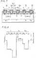
- FIG. 7 is a cross-sectional view illustrating a structure of the CCD delay line according to another embodiment of the present invention.
- like parts corresponding to those of FIG. 3 are marked with the same references and therefore need not be described.
- a channel length L Sa of the storage gate electrode 4 in the charge transfer section 3 k formed at the rear stage of the intermediate output section 7 is set to be longer than a channel length L Sb of the storage gate electrode 4 in the charge transfer section 3 k-1 formed at the front stage of the intermediate output section 7.
- the potential barrier under the transfer gate electrode 5 in the charge transfer section 3k formed at the rear stage of the intermediate output section 7 is affected in a three-dimensional fashion when the potential becomes deep in the storage state of the intermediate output section 7 so that, even if the original potential shown by a phantom in FIG. 8 is changed as shown by a solid line in FIG. 8, the maximum electric charge amount treated in the storage gate electrode 4 of the charge transfer section 3 k is larger as compared with others because the channel length L Sa of the storage gate electrode 4 in the charge transfer section 3 k is longer.
- the CCD delay line can be densified without deteriorating the charge transfer efficiency by reducing the channel lengths of the storage gate electrodes 4 and the transfer gate electrodes 5 in the charge transfer section other than the charge transfer section 3 k provided at the rear stage of the intermediate output section 7.
- the channel length to be reduced is not limited to one of those of the storage gate electrode 4 and the transfer gate electrode 5 and both of the channel lengths of the storage gate electrode 4 and the transfer gate electrode 5 may be set to be similar, which can be expected to achieve great effects as compared with the case such that one of the channel lengths is set to be longer than another.
- the present invention is applied to the CCD delay line in which the floating gate is employed in the intermediate output section as described above in the first and second embodiments, the present invention is not limited thereto and can also be applied to a CCD delay line in which a floating diffusion gate is employed as the intermediate output section.
- the channel length L Ta or L Sa of each of the gate electrodes in the charge transfer section 3 k provided at the rear stage of the intermediate output section 7 is set to be longer than that of each of gate electrodes in the charge transfer section 3 k-1 provided at the front stage of the intermediate output section 7 as described above in the first and second embodiments
- the present invention is not limited to the length of the channel length L Ta or L Sa and such a variant also is possible that a width W (see FIG. 4) in the quadrature direction with respect to the charge transfer direction is set to be larger.
- the maximum charge amount treated in the charge transfer section 3 k provided at the rear stage of the intermediate output section 7 may be increased by increasing a cross-sectional area of each of the channels.
- the impurity concentration of the N ⁇ region in the silicon semiconductor substrate 1 corresponding to the transfer gate electrode 5 in the charge transfer section 3 k provided at the rear stage of the intermediate output section 7 is selected to be lower than that in the charge transfer section 3 k-1 provided at the front stage of the intermediate output section 7, thereby the potential barrier being made higher.
- the maximum charge amount treated in the charge transfer section 3 k can be increased.
- the CCD delay line of the present invention since at least one of the cross-sectional areas of the transfer gate electrode and the storage gate electrode in the charge transfer section provided at the rear stage of the intermediate output section is large than that in the charge transfer section provided at the front stage of the intermediate output section, the charge amount treated in the charge transfer section provided at the rear stage of the intermediate output section can be secured, thus making it possible to make the CCD delay line densified without deteriorating the charge transfer efficiency.
- the CCD delay line can be densified without deteriorating the charge transfer efficiency.
Landscapes
- Engineering & Computer Science (AREA)
- Power Engineering (AREA)
- Microelectronics & Electronic Packaging (AREA)
- Physics & Mathematics (AREA)
- Condensed Matter Physics & Semiconductors (AREA)
- General Physics & Mathematics (AREA)
- Computer Hardware Design (AREA)
- Ceramic Engineering (AREA)
- Electromagnetism (AREA)
- Solid State Image Pick-Up Elements (AREA)
- Transforming Light Signals Into Electric Signals (AREA)
Abstract
Description
- The present invention generally relates to CCD (charge coupled device) delay lines and, more particularly, is directed to a CCD delay line which employs a floating gate (FG) or a floating diffusion gate at its intermediate output portion.
- CCD delay lines are devices which make effective use of charge transfer and/or time operation function to delay or vary a signal from a timing standpoint, thereby processing a signal. The CCD delay line is different from a CCD image pickup element in that signal charges are calculated by an input signal voltage and injected while signal charges are generated and injected by the incidence of light according to the CCD image pickup element. A delay time (delay amount) Td of this CCD delay line is calculated by the following equation:

where N is the number of transfer stages and fc the sampling frequency. - In the case of the device in which the transfer stage N is 680 [bit] and the sampling frequency fc is 10.73 [MHz], the delay time Td thereof is expressed as:

This delay time Td becomes substantially equal to the horizontal synchronizing frequency of a television signal. Further, if the sampling frequency fc is variable, then the delay time Td also becomes variable so that the signal can be compressed and/or expanded from a time base standpoint. - FIG. 1 is a cross-sectional view illustrating an example of a structure of a CCD delay line employing a floating gate (FG) according to the prior art.
- As shown in FIG. 1, a plurality of stages (n stages) of charge transfer units 3n, each formed of an electrode pair of a
storage gate electrode 4 and atransfer gate electrode 5 are sequentially arrayed and at least oneintermediate output portion 7 for deriving a signal of a predetermined delay time is provided to the rear stage of, for example, a (k-1)'th stage of an electric charge transfer section 3k-1 from the signal input side. In this case, regardless of the front and/or rear stage of theintermediate output portion 7, channel lengths and channel widths of thestorage gate electrode 4 and thetransfer gate electrode 5 are set to be the same. Further, the channel lengths of thestorage gate electrode 4 and thetransfer gate electrode 5 tend to be reduced as the CCD delay line becomes more and more densified. - However, if the channel lengths of the
storage gate electrode 4 and thetransfer gate electrode 5 of each of the charge transfer sections 3 are reduced as the CCD delay line becomes more and more densified, then when a potential becomes deep in the storage state of theintermediate output section 7 as shown by a solid line in FIG. 2, a potential barrier beneath thetransfer electrode 5 in a charge transfer section 3k provided at the rear stage of theintermediate output portion 7 is affected in a three-dimensional fashion. As a consequence, an original potential shown by a one-dot chain line in FIG. 2 is changed as shown by the solid line so that a sufficient potential for transferring and storing all electric charges from theintermediate output section 7 cannot be secured. - In other words, while the CCD delay line is made more and more densified by reducing the channel lengths of the
storage gate electrode 4 and thetransfer gate electrode 5 of each of the charge transfer sections 3, the potential barrier under thetransfer gate electrode 5 in the charge transfer section 3k provided at the rear stage of theintermediate output section 7 is changed by the influence of the potential at the front stage of theintermediate output section 7 so that the amount of the electric charges treated in the charge transfer section 3k provided at the rear stage of theintermediate output section 7 is reduced, thereby deteriorating the charge transfer efficiency. - Therefore, it is an object of the present invention to provide an improved CCD delay line in which the aforesaid shortcomings and disadvantages encountered with the prior art can be eliminated.
- More specifically, it is an object of the present invention to provide a CCD delay line in which an amount of charges treated in a charge transfer section provided at the rear stage of an intermediate output section is secured to thereby prevent a charge transfer efficiency from being deteriorated.
- As an aspect of the present invention, in a charge transfer device having charge transfer sections of a plurality of stages, each consisting of an electrode pair of a transfer gate electrode and a storage gate electrode and at least one intermediate output section provided at the rear stage of the charge transfer section of the predetermined stage from the signal input side, at least one of the cross-sectional areas of the transfer gate electrode and the storage gate electrode in the charge transfer section provided at the rear stage of the intermediate output section is selected to be larger than that in the charge transfer section provided at the front stage of the intermediate output section.
- In accordance with another aspect of the present invention, the impurity concentration of the region of the semiconductor substrate opposing to the transfer gate electrode in the charge transfer section provided at the rear stage of the intermediate output section is selected to be lower than that in the charge transfer section provided at the front stage of the intermediate output section, thereby to make the potential barrier higher.
- Therefore, according to the CCD delay line of the present invention, even if the potential barrier under the transfer gate electrode in the charge transfer section provided at the rear stage of the intermediate output section is affected, for example, in a three-dimensional fashion when the potential becomes deep in the storage state of the intermediate output section, the cross-sectional area of the transfer gate electrode in the charge transfer section provided at the rear stage of the intermediate output section is large so that the potential barrier sufficient for transferring and storing all charges from the intermediate output section can be secured. Further, even if the potential barrier is changed, the cross-sectional area of the storage gate electrode in the charge transfer section provided at the rear stage of the intermediate output section is large so that the maximum charge amount treated in the charge transfer section provided at the rear stage of the intermediate output section can be secured. Furthermore, since the impurity concentration in the region of the semiconductor substrate corresponding to the transfer gate electrode in the charge transfer section provided at the rear stage of the intermediate output section is selected to be lower than that in the charge transfer section provided at the front stage of the intermediate output section so as to increase the potential barrier, the maximum charge amount treated in the charge transfer section provided at the rear stage of the intermediate output section can be increased. Therefore, in any case, the charge transfer efficiency can be prevented from being deteriorated as the CCD delay line becomes more and more densified.
- The preceding and other objects, features and advantages of the present invention will become apparent from the following detailed description of illustrative embodiments thereof to be read in conjunction with the accompanying drawings, in which like reference numerals are used to identify the same or similar parts in the several views.
-
- FIG. 1 is a cross-sectional view illustrating an example of a CCD delay line according to the prior art;
- FIG. 2 is a potential diagram of an intermediate output section and to which references will be made in explaining the example shown in FIG. 1;
- FIG. 3 is a cross-sectional view illustrating an embodiment of a CCD delay line according to the present invention;
- FIG. 4 is a plan view illustrating the embodiment of the CCD delay line according to the present invention;
- FIG. 5 is a timing waveform diagram used to explain operation of the present invention;
- FIG. 6 is a potential diagram of an intermediate output unit and to which references will be made in explaining operation of the present invention;
- FIG. 7 is a cross-sectional view illustrating another embodiment of the CCD delay line according to the present invention; and
- FIG. 8 is a potential diagram used to explain operation of the CCD delay line shown in FIG. 7.
- The present invention will hereinafter be described in detail with reference to the accompanying drawings.
- FIG. 3 is a cross-sectional view illustrating a structure of a CCD delay line to which the embodiment of the present invention is applied. FIG. 4 is a plan view thereof.
- As illustrated, charge transfer sections 3 (3₁, ..., 3k, ..., 3n) of n stages are sequentially arrayed, for example, on a
silicon semiconductor substrate 1 through aninsulating layer 2 made of a silicon oxide layer SiO₂ in the transfer direction. Each of the charge transfer sections 3 is formed as a bi-layer structure consisting of an electrode pair of astorage gate electrode 4 made of a first polysilicon layer and atransfer gate electrode 5 made of a second polysilicon layer. The electrode pair of thestorage gate electrode 4 and thetransfer gate electrode 5 are covered with aninsulating layer 6 made of a silicon oxide layer SiO₂ and are thereby insulated from the adjacent electrode pair. These charge transfer sections 3 are applied with two-phase transfer clocks φ₁ and φ₂ at every other pair. - At the rear stage of a charge transfer section 3k-1 of a predetermined stage ((k-1)'th stage in this embodiment) from the signal input side, an
intermediate output section 7 is provided to derive a signal whose delay time is determined by the number of stages. Theintermediate output section 7 is comprised of an output gate (OG)electrode 8, a floating gate (FG)electrode 9 and atransfer gate electrode 10 and astorage gate electrode 11 constructing a precharge gate (PG) section. A signal charge stored in the floating gate (FG) is delivered as a signal output OUT which is delayed by a delay time corresponding to the present stage number k-1. Thetransfer gate electrode 10 and thestorage gate electrode 11 forming the precharge gate section are applied with a precharge clock φPG in a timing relation relative to the transfer clocks φ₁, φ₂ as shown in FIG. 5. A peak value VDD2 of the precharge clock φPG is set to be higher than a peak value VDD1 of the transfer clocks φ₁ and φ₂. N type regions are formed on the surface side of thesilicon semiconductor substrate 1 in an opposing relation to the respectivestorage gate electrodes transfer gate electrodes - In the CCD delay line thus arranged, one of the most specific features of this embodiment lies in that a channel length LTa of the
transfer gate electrode 5 of the charge transfer section 3k formed at the rear stage of theintermediate output section 7 is set to be longer than a channel length LTb of thetransfer gate electrode 5 of the charge transfer section 3k-1 formed at the front stage of theintermediate output section 7. - According to the above-mentioned arrangement, in a schematic diagram of FIG. 6 showing a potential of the
intermediate output section 7 at a time T in FIG. 5, even if a potential barrier under thetransfer gate electrode 5 in the charge transfer section 3k formed at the rear stage of theintermediate output section 7 is affected in a three-dimensional fashion when the potential becomes deep in the storage state of theintermediate output section 7, a potential barrier sufficient for transferring and storing all electric charges from theintermediate output section 7 can be secured. Accordingly, since the electric charge amount treated in the charge transfer section 3k formed at the rear stage of theintermediate output section 7 can be secured, the CCD delay line can be densified without deteriorating the charge transfer efficiency by reducing the channel lengths of thestorage gate electrodes 4 and thetransfer gate electrodes 5 of the charge transfer section other than the charge transfer sectioni 3k formed at the rear stage of theintermediate output section 7. - FIG. 7 is a cross-sectional view illustrating a structure of the CCD delay line according to another embodiment of the present invention. In FIG. 7, like parts corresponding to those of FIG. 3 are marked with the same references and therefore need not be described.
- One of the most specific features of the second embodiment of the invention lies in that a channel length LSa of the
storage gate electrode 4 in the charge transfer section 3k formed at the rear stage of theintermediate output section 7 is set to be longer than a channel length LSb of thestorage gate electrode 4 in the charge transfer section 3k-1 formed at the front stage of theintermediate output section 7. - According to this arrangement, in a schematic diagram of FIG. 8 showing a potential of the
intermediate output section 7 at the time T in FIG. 5, the potential barrier under thetransfer gate electrode 5 in thecharge transfer section 3k formed at the rear stage of theintermediate output section 7 is affected in a three-dimensional fashion when the potential becomes deep in the storage state of theintermediate output section 7 so that, even if the original potential shown by a phantom in FIG. 8 is changed as shown by a solid line in FIG. 8, the maximum electric charge amount treated in thestorage gate electrode 4 of the charge transfer section 3k is larger as compared with others because the channel length LSa of thestorage gate electrode 4 in the charge transfer section 3k is longer. Therefore, the CCD delay line can be densified without deteriorating the charge transfer efficiency by reducing the channel lengths of thestorage gate electrodes 4 and thetransfer gate electrodes 5 in the charge transfer section other than the charge transfer section 3k provided at the rear stage of theintermediate output section 7. - While one of the channel lengths of the
storage gate electrode 4 and thetransfer gate electrode 5 in the charge transfer section 3k provided at the rear stage of theintermediate output section 7 is made longer than that of the charge transfer section 3k-1 provided at the front stage of theintermediate output section 7 as described above in the first and second embodiments, the channel length to be reduced is not limited to one of those of thestorage gate electrode 4 and thetransfer gate electrode 5 and both of the channel lengths of thestorage gate electrode 4 and thetransfer gate electrode 5 may be set to be similar, which can be expected to achieve great effects as compared with the case such that one of the channel lengths is set to be longer than another. - While the present invention is applied to the CCD delay line in which the floating gate is employed in the intermediate output section as described above in the first and second embodiments, the present invention is not limited thereto and can also be applied to a CCD delay line in which a floating diffusion gate is employed as the intermediate output section.
- Further, while the channel length LTa or LSa of each of the gate electrodes in the charge transfer section 3k provided at the rear stage of the
intermediate output section 7 is set to be longer than that of each of gate electrodes in the charge transfer section 3k-1 provided at the front stage of theintermediate output section 7 as described above in the first and second embodiments, the present invention is not limited to the length of the channel length LTa or LSa and such a variant also is possible that a width W (see FIG. 4) in the quadrature direction with respect to the charge transfer direction is set to be larger. In short, it is sufficient that the maximum charge amount treated in the charge transfer section 3k provided at the rear stage of theintermediate output section 7 may be increased by increasing a cross-sectional area of each of the channels. - Alternatively, it is sufficient that the impurity concentration of the N⁻ region in the
silicon semiconductor substrate 1 corresponding to thetransfer gate electrode 5 in the charge transfer section 3k provided at the rear stage of theintermediate output section 7 is selected to be lower than that in the charge transfer section 3k-1 provided at the front stage of theintermediate output section 7, thereby the potential barrier being made higher. Thus, the maximum charge amount treated in the charge transfer section 3k can be increased. - As set out above, according to the CCD delay line of the present invention, since at least one of the cross-sectional areas of the transfer gate electrode and the storage gate electrode in the charge transfer section provided at the rear stage of the intermediate output section is large than that in the charge transfer section provided at the front stage of the intermediate output section, the charge amount treated in the charge transfer section provided at the rear stage of the intermediate output section can be secured, thus making it possible to make the CCD delay line densified without deteriorating the charge transfer efficiency.
- Further, since the charge amount treated in the charge transfer section provided at the rear stage of the intermediate output section can be secured also in the case such that the impurity concentration of the region on the semiconductor substrate corresponding to the transfer gate electrode in the charge transfer section provided at the rear stage of the intermediate output section is selected lower than that in the charge transfer section at the front stage of the intermediate output section, the CCD delay line can be densified without deteriorating the charge transfer efficiency.
- Having described the preferred embodiments of the invention with reference to the accompanying drawings, it is to be understood that the present invention is not limited to those precise embodiments and that various changes and modifications thereof could be effected by one skilled in the art without departing from the spirit or scope of the novel concepts of the invention as defined in the appended claims.
Claims (6)
- A CCD delay line comprising:(a) a first set of charge transfer section (3K) consisting of a plurality of transfer electrodes and a plurality of storage electrodes provided on a CCD channel region through an insulating layer (2), in which a pair of transfer electrode and storage electrode form one delay stage;(b) a second set of charge transfer section (3K) consisting of a plurality of transfer electrodes and a plurality of storage electrodes provided on said CCD channel region through said insulating layer, in which a pair of transfer electrode and storage electrode form another delay stage; and(c) an intermediate output means (7) provided between said first and second sets of charge transfer sections, wherein the cross-sectional area of one of the last pair of transfer electrode (5) and storage electrode (4) of said first set of charge transfer section is smaller than that of one of the first pair of transfer electrode and storage electrode of said second set of charge transfer section.
- A CCD delay line according to claim 1, in which the width in the charge transfer direction of one of the last pair of transfer electrode and storage electrode of said first set of charge transfer section is smaller than that of one of the first pair of transfer and storage electrode of said second set of charge transfer section.
- A CCD delay line according to claim 1, in which the width in quadrature direction with respect to the charge transfer direction of one of the last pair of transfer electrode and storage electrode of said first set of charge transfer section is smaller than that of one of the first pair of transfer and storage electrodes of said second set of charge transfer section.
- A CCD delay line comprising:(1) a first set of charge transfer section consisting of a plurality of transfer electrodes and a plurality of storage electrodes provided on a CCD channel region through an insulating layer, in which a pair of transfer electrode and storage electrode form one delay stage;(2) a second set of charge transfer section consisting of a plurality of transfer electrodes and a plurality of storage electrodes provided on said CCD channel region through said insulating layer, in which a pair of transfer electrodes and storage electrode form another delay stage; and(3) an intermediate output means provided between said first and second sets of charge transfer sections, wherein the impurity concentration of the CCD channel region corresponding to one of the last pair of transfer electrode and storage electrode of said first set of charge transfer section is higher than that of one of the first pair of transfer and storage electrodes of said second set of charge transfer section.
- A CCD delay line according to claim 1 or 2, in which said intermediate output means is formed in a floating-gage type.
- A CCD delay line according to claim 1 or 2, in which said intermediate output means is formed in a floating-diffusion type.
Applications Claiming Priority (2)
| Application Number | Priority Date | Filing Date | Title |
|---|---|---|---|
| JP03023951A JP3141401B2 (en) | 1991-01-23 | 1991-01-23 | Charge transfer device |
| JP23951/91 | 1991-01-23 |
Publications (3)
| Publication Number | Publication Date |
|---|---|
| EP0496357A2 true EP0496357A2 (en) | 1992-07-29 |
| EP0496357A3 EP0496357A3 (en) | 1993-05-05 |
| EP0496357B1 EP0496357B1 (en) | 1995-09-13 |
Family
ID=12124861
Family Applications (1)
| Application Number | Title | Priority Date | Filing Date |
|---|---|---|---|
| EP92100939A Expired - Lifetime EP0496357B1 (en) | 1991-01-23 | 1992-01-21 | Charge coupled device |
Country Status (5)
| Country | Link |
|---|---|
| US (1) | US5227650A (en) |
| EP (1) | EP0496357B1 (en) |
| JP (1) | JP3141401B2 (en) |
| KR (1) | KR100214040B1 (en) |
| DE (1) | DE69204692T2 (en) |
Families Citing this family (7)
| Publication number | Priority date | Publication date | Assignee | Title |
|---|---|---|---|---|
| KR940010932B1 (en) * | 1991-12-23 | 1994-11-19 | 금성일렉트론주식회사 | Manufacturing method of ccd image sensor |
| KR950002084A (en) * | 1993-06-22 | 1995-01-04 | 오가 노리오 | Charge transfer device |
| US5514886A (en) * | 1995-01-18 | 1996-05-07 | Eastman Kodak Company | Image sensor with improved output region for superior charge transfer characteristics |
| US5600696A (en) * | 1995-10-11 | 1997-02-04 | David Sarnoff Research Center, Inc. | Dual-gain floating diffusion output amplifier |
| JP2001308313A (en) * | 2000-04-21 | 2001-11-02 | Nec Corp | Charge transfer device and solid-state image pickup device using it |
| JP4413021B2 (en) * | 2004-01-22 | 2010-02-10 | 三洋電機株式会社 | Semiconductor device and manufacturing method thereof |
| JP4782989B2 (en) * | 2004-05-10 | 2011-09-28 | パナソニック株式会社 | Solid-state imaging device |
Citations (4)
| Publication number | Priority date | Publication date | Assignee | Title |
|---|---|---|---|---|
| US4398301A (en) * | 1980-09-11 | 1983-08-09 | Fairchild Camera & Instrument Corporation | Multiple preamplifiers with intervening overflow cell for charge coupled imaging devices |
| JPS6167963A (en) * | 1984-09-11 | 1986-04-08 | Sanyo Electric Co Ltd | Charge coupling element |
| EP0192142A1 (en) * | 1985-02-15 | 1986-08-27 | Kabushiki Kaisha Toshiba | Charge transfer device |
| FR2581810A1 (en) * | 1985-05-10 | 1986-11-14 | Rca Corp | DELAY LINE WITH LOAD CUTTING DEVICE WITH NON-DESTRUCTIVE LOAD DETECTION USING FLOATING DIFFUSIONS |
Family Cites Families (2)
| Publication number | Priority date | Publication date | Assignee | Title |
|---|---|---|---|---|
| US4513431A (en) * | 1982-06-07 | 1985-04-23 | International Business Machines Corporation | Charge coupled device output circuit structure |
| US4594604A (en) * | 1983-10-21 | 1986-06-10 | Westinghouse Electric Corp. | Charge coupled device with structures for forward scuppering to reduce noise |
-
1991
- 1991-01-23 JP JP03023951A patent/JP3141401B2/en not_active Expired - Fee Related
-
1992
- 1992-01-21 EP EP92100939A patent/EP0496357B1/en not_active Expired - Lifetime
- 1992-01-21 DE DE69204692T patent/DE69204692T2/en not_active Expired - Fee Related
- 1992-01-23 KR KR1019920000884A patent/KR100214040B1/en not_active IP Right Cessation
- 1992-01-23 US US07/824,355 patent/US5227650A/en not_active Expired - Lifetime
Patent Citations (4)
| Publication number | Priority date | Publication date | Assignee | Title |
|---|---|---|---|---|
| US4398301A (en) * | 1980-09-11 | 1983-08-09 | Fairchild Camera & Instrument Corporation | Multiple preamplifiers with intervening overflow cell for charge coupled imaging devices |
| JPS6167963A (en) * | 1984-09-11 | 1986-04-08 | Sanyo Electric Co Ltd | Charge coupling element |
| EP0192142A1 (en) * | 1985-02-15 | 1986-08-27 | Kabushiki Kaisha Toshiba | Charge transfer device |
| FR2581810A1 (en) * | 1985-05-10 | 1986-11-14 | Rca Corp | DELAY LINE WITH LOAD CUTTING DEVICE WITH NON-DESTRUCTIVE LOAD DETECTION USING FLOATING DIFFUSIONS |
Non-Patent Citations (1)
| Title |
|---|
| PATENT ABSTRACTS OF JAPAN vol. 10, no. 236 (E-428)(2292) 15 August 1986 & JP-A-61 067 963 ( SANYO ELECTRIC CO LTD ) 8 April 1986 * |
Also Published As
| Publication number | Publication date |
|---|---|
| DE69204692T2 (en) | 1996-05-09 |
| JPH04239735A (en) | 1992-08-27 |
| EP0496357B1 (en) | 1995-09-13 |
| US5227650A (en) | 1993-07-13 |
| KR100214040B1 (en) | 1999-08-02 |
| EP0496357A3 (en) | 1993-05-05 |
| JP3141401B2 (en) | 2001-03-05 |
| KR920015591A (en) | 1992-08-27 |
| DE69204692D1 (en) | 1995-10-19 |
Similar Documents
| Publication | Publication Date | Title |
|---|---|---|
| IL46895A (en) | C c d memory with interlaced storage | |
| US5040071A (en) | Image sensor having multiple horizontal shift registers | |
| US5608242A (en) | Variable width CCD register with uniform pitch and charge storage capacity | |
| EP0496357B1 (en) | Charge coupled device | |
| US3902186A (en) | Surface charge transistor devices | |
| EP0247503A2 (en) | Method of driving a solid state imager device | |
| US4481538A (en) | Overcoming flicker in field-interlaced CCD imagers with three-phase clocking of the image register | |
| EP0333260A1 (en) | Charge-coupled device | |
| EP0522552B1 (en) | Charge transfer device | |
| US6160580A (en) | CCD image sensor having two-layered electrode structure | |
| US4584697A (en) | Four-phase charge-coupled device having an oversized electrode | |
| US4903284A (en) | Accordion-type charge-coupled devices | |
| US4554675A (en) | Charge transfer device operative at high speed | |
| US5892251A (en) | Apparatus for transferring electric charges | |
| EP0161023B1 (en) | Charge-coupled semiconductor device with dynamic control | |
| US4090095A (en) | Charge coupled device with diode reset for floating gate output | |
| US5303053A (en) | Charge coupled device for overcoming an output voltage difference between different shift registers | |
| EP0732702B1 (en) | Charge transfer apparatus and driving method thereof | |
| JPS5944790B2 (en) | charge coupled device | |
| US5414467A (en) | Charge transfer device wherein the time constant between the clock means and the transfer gate electrodes are substantially equal | |
| JP2524451B2 (en) | HCCD | |
| EP0522436B1 (en) | CCD linear sensor | |
| EP0745997B1 (en) | Charge coupled device with high charge transfer efficiency | |
| US7079183B1 (en) | Charge transfer device for increasing data rate and reducing power consumption | |
| US4868665A (en) | Charge-coupled device with varible storage capacity and constant clock frequency |
Legal Events
| Date | Code | Title | Description |
|---|---|---|---|
| PUAI | Public reference made under article 153(3) epc to a published international application that has entered the european phase |
Free format text: ORIGINAL CODE: 0009012 |
|
| AK | Designated contracting states |
Kind code of ref document: A2 Designated state(s): DE FR GB |
|
| PUAL | Search report despatched |
Free format text: ORIGINAL CODE: 0009013 |
|
| AK | Designated contracting states |
Kind code of ref document: A3 Designated state(s): DE FR GB |
|
| 17P | Request for examination filed |
Effective date: 19931006 |
|
| 17Q | First examination report despatched |
Effective date: 19941122 |
|
| GRAA | (expected) grant |
Free format text: ORIGINAL CODE: 0009210 |
|
| AK | Designated contracting states |
Kind code of ref document: B1 Designated state(s): DE FR GB |
|
| REF | Corresponds to: |
Ref document number: 69204692 Country of ref document: DE Date of ref document: 19951019 |
|
| ET | Fr: translation filed | ||
| PLBE | No opposition filed within time limit |
Free format text: ORIGINAL CODE: 0009261 |
|
| STAA | Information on the status of an ep patent application or granted ep patent |
Free format text: STATUS: NO OPPOSITION FILED WITHIN TIME LIMIT |
|
| 26N | No opposition filed | ||
| REG | Reference to a national code |
Ref country code: GB Ref legal event code: IF02 |
|
| PGFP | Annual fee paid to national office [announced via postgrant information from national office to epo] |
Ref country code: DE Payment date: 20090115 Year of fee payment: 18 |
|
| PGFP | Annual fee paid to national office [announced via postgrant information from national office to epo] |
Ref country code: GB Payment date: 20090121 Year of fee payment: 18 |
|
| PGFP | Annual fee paid to national office [announced via postgrant information from national office to epo] |
Ref country code: FR Payment date: 20090113 Year of fee payment: 18 |
|
| GBPC | Gb: european patent ceased through non-payment of renewal fee |
Effective date: 20100121 |
|
| REG | Reference to a national code |
Ref country code: FR Ref legal event code: ST Effective date: 20100930 |
|
| PG25 | Lapsed in a contracting state [announced via postgrant information from national office to epo] |
Ref country code: FR Free format text: LAPSE BECAUSE OF NON-PAYMENT OF DUE FEES Effective date: 20100201 |
|
| PG25 | Lapsed in a contracting state [announced via postgrant information from national office to epo] |
Ref country code: DE Free format text: LAPSE BECAUSE OF NON-PAYMENT OF DUE FEES Effective date: 20100803 |
|
| PG25 | Lapsed in a contracting state [announced via postgrant information from national office to epo] |
Ref country code: GB Free format text: LAPSE BECAUSE OF NON-PAYMENT OF DUE FEES Effective date: 20100121 |