EP0247503A2 - Method of driving a solid state imager device - Google Patents
Method of driving a solid state imager device Download PDFInfo
- Publication number
- EP0247503A2 EP0247503A2 EP87107292A EP87107292A EP0247503A2 EP 0247503 A2 EP0247503 A2 EP 0247503A2 EP 87107292 A EP87107292 A EP 87107292A EP 87107292 A EP87107292 A EP 87107292A EP 0247503 A2 EP0247503 A2 EP 0247503A2
- Authority
- EP
- European Patent Office
- Prior art keywords
- storage area
- charge storage
- conductivity type
- solid state
- state imager
- Prior art date
- Legal status (The legal status is an assumption and is not a legal conclusion. Google has not performed a legal analysis and makes no representation as to the accuracy of the status listed.)
- Granted
Links
- 239000007787 solid Substances 0.000 title claims abstract description 21
- 239000000758 substrate Substances 0.000 claims abstract description 13
- 239000010410 layer Substances 0.000 description 18
- XUIMIQQOPSSXEZ-UHFFFAOYSA-N Silicon Chemical compound [Si] XUIMIQQOPSSXEZ-UHFFFAOYSA-N 0.000 description 5
- 229910052710 silicon Inorganic materials 0.000 description 5
- 239000010703 silicon Substances 0.000 description 5
- 108091006146 Channels Proteins 0.000 description 4
- VYPSYNLAJGMNEJ-UHFFFAOYSA-N Silicium dioxide Chemical compound O=[Si]=O VYPSYNLAJGMNEJ-UHFFFAOYSA-N 0.000 description 4
- 229910052681 coesite Inorganic materials 0.000 description 2
- 229910052906 cristobalite Inorganic materials 0.000 description 2
- 229910021420 polycrystalline silicon Inorganic materials 0.000 description 2
- 229920005591 polysilicon Polymers 0.000 description 2
- 239000000377 silicon dioxide Substances 0.000 description 2
- 235000012239 silicon dioxide Nutrition 0.000 description 2
- 229910052682 stishovite Inorganic materials 0.000 description 2
- 229910052905 tridymite Inorganic materials 0.000 description 2
- 206010016173 Fall Diseases 0.000 description 1
- 108010075750 P-Type Calcium Channels Proteins 0.000 description 1
- 238000010276 construction Methods 0.000 description 1
- 239000013078 crystal Substances 0.000 description 1
- 230000007547 defect Effects 0.000 description 1
- 238000010586 diagram Methods 0.000 description 1
- 230000000694 effects Effects 0.000 description 1
- 239000012535 impurity Substances 0.000 description 1
- 238000012986 modification Methods 0.000 description 1
- 230000004048 modification Effects 0.000 description 1
- 239000011241 protective layer Substances 0.000 description 1
Images

Classifications
-
- H—ELECTRICITY
- H01—ELECTRIC ELEMENTS
- H01L—SEMICONDUCTOR DEVICES NOT COVERED BY CLASS H10
- H01L27/00—Devices consisting of a plurality of semiconductor or other solid-state components formed in or on a common substrate
- H01L27/14—Devices consisting of a plurality of semiconductor or other solid-state components formed in or on a common substrate including semiconductor components sensitive to infrared radiation, light, electromagnetic radiation of shorter wavelength or corpuscular radiation and specially adapted either for the conversion of the energy of such radiation into electrical energy or for the control of electrical energy by such radiation
- H01L27/144—Devices controlled by radiation
- H01L27/146—Imager structures
- H01L27/148—Charge coupled imagers
- H01L27/14831—Area CCD imagers
Definitions
- This invention relates generally to a solid state imager device and is directed more particularly to an interline transfer type solid state imager device which has a light receiving section formed of a buried channel MOS structure.
- a conventional solid state imager device which can reduce the dark current, for example, is disclosed in a collection of papers presented at '84 National Conference of the Institute of Television Engineers of Japan, on pages 4l-42.
- Such known solid state imager device has a light receiving section which is formed of a buried channel MOS structure. Specifically, the device is constructed such that an n-type charge storage area is formed over the surface of a p-type silicon substrate and a forward electrode is formed on the charge storage area through an insulating layer, so that it can be operated under conditions where a hole storage layer is produced on a boundary between the n-type charge storage area and the insulating layer.
- the forward electrode is applied with a predetermined direct current voltage so as to form a channel within the n-type charge storage area from holes previously stored on the surface of the n-type charge storage area.
- the holes are kept in a so-called pinning state, so as to suppress the generation of hole-electron pairs which are the main component of the dark current from the surface level.
- a solid state imager device as described above can advantageously reduce the dark current.
- the present invention provides a solid state imager device comprising;
- FIGS. l-3 An embodiment of a solid state imager device according to the present invention will be described with reference to FIGS. l-3.
- FIG. l shows a p-type silicon substrate l into which a p-type impurity is diffused with a relatively low concentration. It is assumed in the present embodiment that a light receiving section 5, a vertical register section 6, a horizontal register section (not shown) and an output circuit section (not shown) are all formed on the p-type silicon substrate l. In the structure, a plurality of the light receiving sections 5 are provided which are arranged in the horizontal and vertical directions. The vertical register section 6 is arranged to be parallel to each of the vertically aligned light receiving sections 5, and the vertical register section 6 is arranged to be parallel to the horizontal register section, so as to form an interline transfer solid state imager device.
- the light receiving section 5 comprises an n-type charge storage area 2 on the surface of the p-type silicon substrate l.
- a forward electrode 4 is formed of a light transmissible polysilicon which is deposited over the charge storage area 2 through an insulating layer 3 made of SiO2, so that the light receiving section 5 is formed by the buried channel MOS structure.
- the forward electrode 4 When the solid state imager device of the present embodiment is operated so as to pick up an image, the forward electrode 4 is supplied through a terminal B with a pulse signal ⁇ v, as shown in FIG. 2A.
- a pulse signal ⁇ v When the forward electrode 4 is supplied with a low level voltage V1, e.g. -l2V, a storage layer of holes is formed on the boundary between the charge storage area 2 and the insulating layer 3, and when a high level voltage V2, e.g. 2V is supplied, the depletion layer beneath the charge storage area 2 is extended in the thickness direction of the substrate l.
- V1 low level voltage
- V2V high level voltage
- the pulse signal ⁇ v is selected such that its rising-up edge and its falling-down edge are within a horizontal blanking period so that the image signal is not influenced by the pulse signal ⁇ v.
- n-type overflow drain region 7 is formed adjacent to the charge storage area 2 through a p-type overflow control region 8 so as to prevent so-called blooming where the image picked up is made unclear by excessivee signal charges which are produced when an especially strong light is incident on the imager device, and which flow into other charge storage areas.
- a p-type channel stopper region 9 is arranged adjacent to the overflow drain region 7 as well as in regions between respective charge storage areas which are vertically adjacent to each other.
- the vertical register section 6 is formed of an n-type charge transfer region ll formed on a p-type well region l0 which is selectively formed on the p-type silicon substrate l and a transfer electrode l2 made of polysilicon is formed on the charge transfer region ll through the insulating layer 3.
- the vertical register section 6 is formed as a so-called bulk charge coupled device (BCCD) structure.
- FIG. l shows only one transfer electrode l2.
- the requried number of transfer electrodes l2 are provided so that the vertical register section 6 of the present embodiment is driven in a 4-phase driving manner.
- a gate electrode l3 for controlling the transfer of signal charges which accumulate in the charge storage area 2 to the charge transfer region ll in a manner such that it is integral with a portion of the transfer electrode l2, to thus form a gate section l4.
- the signal charges are transferred from the charge storage area 2 to the charge transfer region ll during a vertical flyback period using a low level voltage V1 which is supplied to the forward electrode 4.
- a light shielding layer l5 made e.g. of Al.
- a protective layer l6 made of SiO2.
- the forward electrode 4 is supplied with the pulse signal ⁇ v as shown in FIG. 2A.
- the forward electrode 4 is supplied with the low level voltage V1
- holes will accumulate on the surface of the charge storage area 2 and the the holes are kept in the pinning state, to suppress hole-electron pair generation from the surface level.
- the forward electrode 4 is supplied with the high level voltage V2
- the holes which have accumulated on the surface of the charge storage area 2 will be released.
- a dark signal such as shown in FIG. 2B will be generated in the charge storage area 2.
- a smear level value when the duty ratio T2/T1 is 0 is defined as l, and the curve illustrates variations in the smear level value as this ratio is varied.
- the present embodiment has advantages over the prior art in that the dark current and smear level can be effectively reduced by using a simple construction such that the forward electrode 4 is alternately supplied with the pulse signal ⁇ v consisting of a low level voltage V1, e.g. -l2V, for accumulating holes on the surface of the charge storage area 2 and a high level voltage V2, e.g. 2V, for extending the depletion layer beneath the charge storage area 2 and by using an appropriate duty ratio in the range of 2 - 5.
- V1 low level voltage
- V2V high level voltage
- a further advantage of the present embodiment is that the dark current from the surface level 8 is not completely suppressed but is produced in a degree such that the quality of the image is not influenced by the dark current which makes it difficult to distinguish minute local dark signals (white flaw), produced by crystal defects and the like and other factors than the surface level, which appear on an image if the dark current is completely suppressed.
- the low level voltage period T1 is determined as one horizontal period and the pulse signal ⁇ v raises and falls within the horizontal blanking period.
- a pulse signal ⁇ v ⁇ which has its low level voltage arranged within the horizontal blanking period, as shown in FIG. 4, may be applied to the forward electorde.
- the duty ratio T2/T1 can be set to have a sufficiently large value so that smear can be satisfactorily suppressed, and so that the surface is not depleted continuously for more than one horizontal period so that the dark current can also be sufficiently suppressed.
- the above described present embodiment is for the case where the signal charges are electrons.
- the present invention may be applied to a case where the signal charges are holes.
- the conductivity types of the respective sections are selected so as to opposite to those shown in FIG. l. The same effects as described above can be obtained in this case.
Abstract
Description
- This invention relates generally to a solid state imager device and is directed more particularly to an interline transfer type solid state imager device which has a light receiving section formed of a buried channel MOS structure.
- In a solid state imager device due to its characteristics, it is desirable to reduce, as much as possible the dark current which may be a source of noise.
- A conventional solid state imager device which can reduce the dark current, for example, is disclosed in a collection of papers presented at '84 National Conference of the Institute of Television Engineers of Japan, on pages 4l-42. Such known solid state imager device has a light receiving section which is formed of a buried channel MOS structure. Specifically, the device is constructed such that an n-type charge storage area is formed over the surface of a p-type silicon substrate and a forward electrode is formed on the charge storage area through an insulating layer, so that it can be operated under conditions where a hole storage layer is produced on a boundary between the n-type charge storage area and the insulating layer. In this solid state imager device, the forward electrode is applied with a predetermined direct current voltage so as to form a channel within the n-type charge storage area from holes previously stored on the surface of the n-type charge storage area. Thus, the holes are kept in a so-called pinning state, so as to suppress the generation of hole-electron pairs which are the main component of the dark current from the surface level. A solid state imager device as described above can advantageously reduce the dark current.
- However, such conventional solid state imager device has disadvantages in that since the forward electrode is always supplied with a direct current voltage so as to store holes on the boundary between the n-type charge storage area and the insulating layer, the depletion layer under the charge storage area is not extended making it impossible to suppress disturbances in images which are picked-up, which disturbances are caused by signal charges flowing from the inside of the substrate into the charge transfer section, which are called "smear".
- Accordingly, it is an object of the present invention to provide a solid state imager device which can effectively suppress dark current as well as smear.
- To achieve the above object, the present invention provides a solid state imager device comprising;
- (a) a substrate of a first conductivity type;
- (b) a charge storage area of a second conductivity type formed on a surface of the substrate of the first conductivity type;
- (c) a forward electrode formed on the charge storage area of the second conductivity type through an insulating layer; and
- (d) a means for alternatively supplying the forward electrode with a first voltage for accumulating charges of a first conductivity type on a boundary between the charge storage area of the second conductivity type and the insulating layer and a second voltage for extending a depletion layer formed beneath the charge storage area of the second conductivity type.
- These and other objects, features and advantages of the present invention will become apparent from the following detailed description of the preferred embodiment taken in conjunction with the accompanying drawings, throughout which like reference numerals designate like elements and parts.
-
- FIG. l is a diagram showing a cross-sectional view of a main portion of a solid state imager device according to the present invention;
- FIGS. 2A and 2B are timing charts showing waveforms of a pulse signal φ v and a dark signal, respectively;
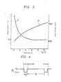
- FIG. 3 is a graph showing the relationship between the duty ratio T₂/T₁ of the pulse signal φ v and a smear level and a relationship between the duty ratio T₂2/T₁ and a dark signal output; and
- FIG. 4 is a chart showing a waveform of a pulse signal φ vʹ.
- An embodiment of a solid state imager device according to the present invention will be described with reference to FIGS. l-3.
- FIG. l shows a p-type silicon substrate l into which a p-type impurity is diffused with a relatively low concentration. It is assumed in the present embodiment that a
light receiving section 5, avertical register section 6, a horizontal register section (not shown) and an output circuit section (not shown) are all formed on the p-type silicon substrate l. In the structure, a plurality of the light receivingsections 5 are provided which are arranged in the horizontal and vertical directions. Thevertical register section 6 is arranged to be parallel to each of the vertically alignedlight receiving sections 5, and thevertical register section 6 is arranged to be parallel to the horizontal register section, so as to form an interline transfer solid state imager device. - The
light receiving section 5 comprises an n-typecharge storage area 2 on the surface of the p-type silicon substrate l. Aforward electrode 4 is formed of a light transmissible polysilicon which is deposited over thecharge storage area 2 through an insulating layer 3 made of SiO₂, so that thelight receiving section 5 is formed by the buried channel MOS structure. - When the solid state imager device of the present embodiment is operated so as to pick up an image, the
forward electrode 4 is supplied through a terminal B with a pulse signal φ v, as shown in FIG. 2A. When theforward electrode 4 is supplied with a low level voltage V₁, e.g. -l2V, a storage layer of holes is formed on the boundary between thecharge storage area 2 and the insulating layer 3, and when a high level voltage V₂, e.g. 2V is supplied, the depletion layer beneath thecharge storage area 2 is extended in the thickness direction of the substrate l. It should be noted that the pulse signal φ v is selected such that its rising-up edge and its falling-down edge are within a horizontal blanking period so that the image signal is not influenced by the pulse signal φ v. - Also, a relatively high concentration n-type
overflow drain region 7 is formed adjacent to thecharge storage area 2 through a p-typeoverflow control region 8 so as to prevent so-called blooming where the image picked up is made unclear by excesive signal charges which are produced when an especially strong light is incident on the imager device, and which flow into other charge storage areas. A p-type channel stopper region 9 is arranged adjacent to theoverflow drain region 7 as well as in regions between respective charge storage areas which are vertically adjacent to each other. - The
vertical register section 6 is formed of an n-type charge transfer region ll formed on a p-type well region l0 which is selectively formed on the p-type silicon substrate l and a transfer electrode l2 made of polysilicon is formed on the charge transfer region ll through the insulating layer 3. Thus, thevertical register section 6 is formed as a so-called bulk charge coupled device (BCCD) structure. FIG. l shows only one transfer electrode l2. However, as is well known in the art, the requried number of transfer electrodes l2 are provided so that thevertical register section 6 of the present embodiment is driven in a 4-phase driving manner. - On the insulating layer 3 between the
light receiving section 5 and thevertical register section 6, there is formed a gate electrode l3 for controlling the transfer of signal charges which accumulate in thecharge storage area 2 to the charge transfer region ll in a manner such that it is integral with a portion of the transfer electrode l2, to thus form a gate section l4. The signal charges are transferred from thecharge storage area 2 to the charge transfer region ll during a vertical flyback period using a low level voltage V₁ which is supplied to theforward electrode 4. - On the upper surface of the
forward electrode 4 except over thelight receiving section 5 there is deposited a light shielding layer l5 made e.g. of Aℓ. Also, over all of theforward electrode 4 there is deposited a protective layer l6 made of SiO₂. - Other sections required for the interline transfer solid state imager device, such as the horizontal register section, the output circuit section are formed in the same manner as the conventionally known device, and these are not shown in FIG. l.
- In the solid state imager device of the present invention constructed as described above, the
forward electrode 4 is supplied with the pulse signal φ v as shown in FIG. 2A. When theforward electrode 4 is supplied with the low level voltage V₁, holes will accumulate on the surface of thecharge storage area 2 and the the holes are kept in the pinning state, to suppress hole-electron pair generation from the surface level. If theforward electrode 4 is supplied with the high level voltage V₂, the holes which have accumulated on the surface of thecharge storage area 2 will be released. However, once the holes accumulate on the surface of thecharge storage area 2, the hole-electron pair generation is suppressed for a predetermined time during which the holes are released. Therefore, if the pulse signal φ v shown in FIG. 2A is applied to theforward electrode 4, a dark signal such as shown in FIG. 2B will be generated in thecharge storage area 2. If the duty ratio T₂/T₁ of the pulse voltage φ v is varied from T₂/T₁ = 0 to T₂/ T₁ l0, the dark current output will increase as indicated by the solid line curve X in FIG. 3. Specifically, the dark current output will be low when the duty ratio T₂/T₁ is smaller, and the dark current output goes higher when the duty ratio T₂/T₁ becomes larger. - When the low level voltage V₁ is supplied to the
forward electrode 4, the depletion layer formed beneath thecharge storage area 2 becomes shallow, which allows smear to be easily produced. On the other hand, when the high level voltage V₂ is supplied to theforward electrode 4, the depletion layer formed beneath thecharge storage area 2 becomes thicker, which suppresses the generation of smear. The solid line curve Y in FIG. 3 shows how the smear level is varied when the duty ratio T₂/T₁ of the pulse voltage φ v is varied from T₂/T₁ = 0 to T₂/T₁ = l0. In FIG. 3, a smear level value when the duty ratio T₂/T₁ is 0 is defined as l, and the curve illustrates variations in the smear level value as this ratio is varied. - As will be understood from a consideration of FIG. 3, it is possible to reduce the dark current as well as the smear level by selecting the duty ratio T₂/T₁ of the pulse signal v to fall in a range of T₂/T₁ = 2 to T₂/T₁ = 5.
- As described above, the present embodiment has advantages over the prior art in that the dark current and smear level can be effectively reduced by using a simple construction such that the
forward electrode 4 is alternately supplied with the pulse signal φ v consisting of a low level voltage V₁, e.g. -l2V, for accumulating holes on the surface of thecharge storage area 2 and a high level voltage V₂, e.g. 2V, for extending the depletion layer beneath thecharge storage area 2 and by using an appropriate duty ratio in the range of 2 - 5. - A further advantage of the present embodiment is that the dark current from the
surface level 8 is not completely suppressed but is produced in a degree such that the quality of the image is not influenced by the dark current which makes it difficult to distinguish minute local dark signals (white flaw), produced by crystal defects and the like and other factors than the surface level, which appear on an image if the dark current is completely suppressed. - The above described embodiment is for a case where the low level voltage period T₁ is determined as one horizontal period and the pulse signal φ v raises and falls within the horizontal blanking period. Alternatively, a pulse signal φ vʹ which has its low level voltage arranged within the horizontal blanking period, as shown in FIG. 4, may be applied to the forward electorde. In this case, the duty ratio T₂/T₁ can be set to have a sufficiently large value so that smear can be satisfactorily suppressed, and so that the surface is not depleted continuously for more than one horizontal period so that the dark current can also be sufficiently suppressed.
- The above described present embodiment is for the case where the signal charges are electrons. However, the present invention may be applied to a case where the signal charges are holes. For that case, the conductivity types of the respective sections are selected so as to opposite to those shown in FIG. l. The same effects as described above can be obtained in this case.
- The above description is for a single preferred embodiment of the invention but it will be apparent that many modifications and variations could be effected by one skilled in the art without departing from the spirit or scope of the nvoel concepts of the invention and the scope of the invention should be determined only by the appended claims.
Claims (3)
Applications Claiming Priority (2)
| Application Number | Priority Date | Filing Date | Title |
|---|---|---|---|
| JP61114375A JPS62269357A (en) | 1986-05-19 | 1986-05-19 | Solid-state image sensing device |
| JP114375/86 | 1986-05-19 |
Publications (3)
| Publication Number | Publication Date |
|---|---|
| EP0247503A2 true EP0247503A2 (en) | 1987-12-02 |
| EP0247503A3 EP0247503A3 (en) | 1990-04-04 |
| EP0247503B1 EP0247503B1 (en) | 1995-03-01 |
Family
ID=14636115
Family Applications (1)
| Application Number | Title | Priority Date | Filing Date |
|---|---|---|---|
| EP87107292A Expired - Lifetime EP0247503B1 (en) | 1986-05-19 | 1987-05-19 | Method of driving a solid state imager device |
Country Status (5)
| Country | Link |
|---|---|
| US (1) | US4794279A (en) |
| EP (1) | EP0247503B1 (en) |
| JP (1) | JPS62269357A (en) |
| KR (1) | KR960004467B1 (en) |
| DE (1) | DE3751102T2 (en) |
Cited By (2)
| Publication number | Priority date | Publication date | Assignee | Title |
|---|---|---|---|---|
| EP0332173A2 (en) * | 1988-03-08 | 1989-09-13 | Kabushiki Kaisha Toshiba | Solid-state image pickup device |
| EP0399601A1 (en) * | 1989-05-23 | 1990-11-28 | Koninklijke Philips Electronics N.V. | Dark current reduction in buried channel charge coupled imaging device |
Families Citing this family (14)
| Publication number | Priority date | Publication date | Assignee | Title |
|---|---|---|---|---|
| JPH01125074A (en) * | 1987-11-10 | 1989-05-17 | Fuji Photo Film Co Ltd | Solid-state image pickup device |
| JPH0766961B2 (en) * | 1988-10-07 | 1995-07-19 | 三菱電機株式会社 | Solid-state image sensor |
| JPH02309877A (en) * | 1989-05-25 | 1990-12-25 | Sony Corp | Solid-state image pickup device |
| US5528643A (en) * | 1989-11-13 | 1996-06-18 | Texas Instruments Incorporated | Charge coupled device/charge super sweep image system and method for making |
| US5182623A (en) * | 1989-11-13 | 1993-01-26 | Texas Instruments Incorporated | Charge coupled device/charge super sweep image system and method for making |
| JP2738589B2 (en) * | 1990-09-05 | 1998-04-08 | 三菱電機株式会社 | Solid-state imaging device |
| JP2690612B2 (en) * | 1990-10-05 | 1997-12-10 | キヤノン株式会社 | Photoelectric conversion device |
| US5329149A (en) * | 1990-10-12 | 1994-07-12 | Seiko Instruments Inc. | Image sensor with non-light-transmissive layer having photosensing windows |
| JP2500428B2 (en) * | 1993-04-06 | 1996-05-29 | 日本電気株式会社 | Image sensor and driving method thereof |
| US5757427A (en) * | 1993-04-23 | 1998-05-26 | Hamamatsu Photonics K.K. | Image pick-up apparatus having a charge coupled device with multiple electrodes, a buffer layer located below some of the electrodes |
| JPH08264747A (en) * | 1995-03-16 | 1996-10-11 | Eastman Kodak Co | Solid-state picturization device having container-lateral-side overflow-drain inplant,and its manufacture |
| JP2005348061A (en) * | 2004-06-02 | 2005-12-15 | Sanyo Electric Co Ltd | Electronic camera |
| EP1608019B1 (en) * | 2004-06-15 | 2010-02-24 | STMicroelectronics (Research & Development) Limited | Imaging sensor |
| JP5648923B2 (en) * | 2009-10-09 | 2015-01-07 | 国立大学法人静岡大学 | Semiconductor element and solid-state imaging device |
Citations (1)
| Publication number | Priority date | Publication date | Assignee | Title |
|---|---|---|---|---|
| EP0173542A2 (en) * | 1984-08-28 | 1986-03-05 | Sharp Kabushiki Kaisha | A solid-state image sensor |
Family Cites Families (4)
| Publication number | Priority date | Publication date | Assignee | Title |
|---|---|---|---|---|
| JPS5323224A (en) * | 1976-08-16 | 1978-03-03 | Hitachi Ltd | Solid pickup unit |
| JPH0795827B2 (en) * | 1985-07-22 | 1995-10-11 | 株式会社ニコン | Camera drive |
| JPS61219271A (en) * | 1985-03-25 | 1986-09-29 | Nippon Kogaku Kk <Nikon> | Method for driving inter-line transfer type ccd |
| US4743778A (en) * | 1985-03-25 | 1988-05-10 | Nippon Kogaku K. K. | Solid-state area imaging device having interline transfer CCD |
-
1986
- 1986-05-19 JP JP61114375A patent/JPS62269357A/en active Pending
-
1987
- 1987-05-18 KR KR1019870004874A patent/KR960004467B1/en not_active IP Right Cessation
- 1987-05-18 US US07/050,400 patent/US4794279A/en not_active Expired - Lifetime
- 1987-05-19 EP EP87107292A patent/EP0247503B1/en not_active Expired - Lifetime
- 1987-05-19 DE DE3751102T patent/DE3751102T2/en not_active Expired - Fee Related
Patent Citations (1)
| Publication number | Priority date | Publication date | Assignee | Title |
|---|---|---|---|---|
| EP0173542A2 (en) * | 1984-08-28 | 1986-03-05 | Sharp Kabushiki Kaisha | A solid-state image sensor |
Non-Patent Citations (2)
| Title |
|---|
| 1984 National Conference of the Institute of Television Engineers of Japan, pages 41,42; M.MONOI et al.:"Improvement of image lag in large area photosensing elements" * |
| INTERNATIONAL ELECTRON DEVICES MEETING, San Francisco, 9th-12th December 1984, pages 28-31, IEEE, New York, US; B.C. BURKEY et al.: "The pinned photodiode for an interline-transfer CCD image sensor" * |
Cited By (3)
| Publication number | Priority date | Publication date | Assignee | Title |
|---|---|---|---|---|
| EP0332173A2 (en) * | 1988-03-08 | 1989-09-13 | Kabushiki Kaisha Toshiba | Solid-state image pickup device |
| EP0332173A3 (en) * | 1988-03-08 | 1991-03-06 | Kabushiki Kaisha Toshiba | Solid-state image pickup device |
| EP0399601A1 (en) * | 1989-05-23 | 1990-11-28 | Koninklijke Philips Electronics N.V. | Dark current reduction in buried channel charge coupled imaging device |
Also Published As
| Publication number | Publication date |
|---|---|
| KR960004467B1 (en) | 1996-04-06 |
| EP0247503A3 (en) | 1990-04-04 |
| US4794279A (en) | 1988-12-27 |
| DE3751102D1 (en) | 1995-04-06 |
| KR880014678A (en) | 1988-12-24 |
| DE3751102T2 (en) | 1995-10-12 |
| EP0247503B1 (en) | 1995-03-01 |
| JPS62269357A (en) | 1987-11-21 |
Similar Documents
| Publication | Publication Date | Title |
|---|---|---|
| US4774586A (en) | Interline type charge transfer imaging device | |
| US4322753A (en) | Smear and/or blooming in a solid state charge transfer image pickup device | |
| US4484210A (en) | Solid-state imaging device having a reduced image lag | |
| US4717945A (en) | Solid state image pick-up device with a shutter function | |
| EP0247503B1 (en) | Method of driving a solid state imager device | |
| EP0224993A1 (en) | A method of operating a solid-state image sensor | |
| US5962882A (en) | Charge coupled devices including buried transmission gates | |
| US4242599A (en) | Charge transfer image sensor with antiblooming and exposure control | |
| US4485315A (en) | Blooming suppression in a CCD imaging device | |
| US4672455A (en) | Solid-state image-sensor having reverse-biased substrate and transfer registers | |
| US4462047A (en) | Solid state imager with blooming suppression | |
| CA1193711A (en) | Solid state image sensor | |
| US4748486A (en) | Solid-state image sensor | |
| JPS6262553A (en) | Solid state image pick-up device | |
| US5402459A (en) | Frame transfer image sensor with electronic shutter | |
| US5426317A (en) | Frame interline transfer CCD imager | |
| GB2128052A (en) | Flicker reduction in field-interlaced three-phase clocked ccd imagers | |
| US4584697A (en) | Four-phase charge-coupled device having an oversized electrode | |
| US5760430A (en) | Charge transfer device and solid-state imaging apparatus using the same device | |
| US6891243B2 (en) | Solid-state image pick-up device | |
| EP0499275A1 (en) | Solid state imager | |
| KR101293586B1 (en) | Solid-state image pickup device and driving method of solid-state image pickup device | |
| CN101794803B (en) | Solid-state image capturing apparatus, driving method thereof and electronic apparatus | |
| US4837629A (en) | Image pickup method using a CCD-type solid state image pickup device with charge dissipation | |
| US5907356A (en) | Solid-state image pickup device |
Legal Events
| Date | Code | Title | Description |
|---|---|---|---|
| PUAI | Public reference made under article 153(3) epc to a published international application that has entered the european phase |
Free format text: ORIGINAL CODE: 0009012 |
|
| AK | Designated contracting states |
Kind code of ref document: A2 Designated state(s): DE FR GB NL |
|
| PUAL | Search report despatched |
Free format text: ORIGINAL CODE: 0009013 |
|
| AK | Designated contracting states |
Kind code of ref document: A3 Designated state(s): DE FR GB NL |
|
| 17P | Request for examination filed |
Effective date: 19900927 |
|
| 17Q | First examination report despatched |
Effective date: 19920515 |
|
| GRAA | (expected) grant |
Free format text: ORIGINAL CODE: 0009210 |
|
| AK | Designated contracting states |
Kind code of ref document: B1 Designated state(s): DE FR GB NL |
|
| REF | Corresponds to: |
Ref document number: 3751102 Country of ref document: DE Date of ref document: 19950406 |
|
| ET | Fr: translation filed | ||
| PLBE | No opposition filed within time limit |
Free format text: ORIGINAL CODE: 0009261 |
|
| STAA | Information on the status of an ep patent application or granted ep patent |
Free format text: STATUS: NO OPPOSITION FILED WITHIN TIME LIMIT |
|
| 26N | No opposition filed | ||
| REG | Reference to a national code |
Ref country code: GB Ref legal event code: IF02 |
|
| PGFP | Annual fee paid to national office [announced via postgrant information from national office to epo] |
Ref country code: FR Payment date: 20030508 Year of fee payment: 17 |
|
| PGFP | Annual fee paid to national office [announced via postgrant information from national office to epo] |
Ref country code: GB Payment date: 20030514 Year of fee payment: 17 |
|
| PGFP | Annual fee paid to national office [announced via postgrant information from national office to epo] |
Ref country code: DE Payment date: 20030529 Year of fee payment: 17 |
|
| PGFP | Annual fee paid to national office [announced via postgrant information from national office to epo] |
Ref country code: NL Payment date: 20030530 Year of fee payment: 17 |
|
| PG25 | Lapsed in a contracting state [announced via postgrant information from national office to epo] |
Ref country code: GB Free format text: LAPSE BECAUSE OF NON-PAYMENT OF DUE FEES Effective date: 20040519 |
|
| PG25 | Lapsed in a contracting state [announced via postgrant information from national office to epo] |
Ref country code: NL Free format text: LAPSE BECAUSE OF NON-PAYMENT OF DUE FEES Effective date: 20041201 Ref country code: DE Free format text: LAPSE BECAUSE OF NON-PAYMENT OF DUE FEES Effective date: 20041201 |
|
| GBPC | Gb: european patent ceased through non-payment of renewal fee |
Effective date: 20040519 |
|
| PG25 | Lapsed in a contracting state [announced via postgrant information from national office to epo] |
Ref country code: FR Free format text: LAPSE BECAUSE OF NON-PAYMENT OF DUE FEES Effective date: 20050131 |
|
| NLV4 | Nl: lapsed or anulled due to non-payment of the annual fee |
Effective date: 20041201 |
|
| REG | Reference to a national code |
Ref country code: FR Ref legal event code: ST |