EP0495202A2 - Dispositif pour changer une onde optique avec un petit diamètre du mode en une onde avec un diamètre plus grand - Google Patents
Dispositif pour changer une onde optique avec un petit diamètre du mode en une onde avec un diamètre plus grand Download PDFInfo
- Publication number
- EP0495202A2 EP0495202A2 EP91121196A EP91121196A EP0495202A2 EP 0495202 A2 EP0495202 A2 EP 0495202A2 EP 91121196 A EP91121196 A EP 91121196A EP 91121196 A EP91121196 A EP 91121196A EP 0495202 A2 EP0495202 A2 EP 0495202A2
- Authority
- EP
- European Patent Office
- Prior art keywords
- waveguide
- optical
- optical wave
- face
- wave
- Prior art date
- Legal status (The legal status is an assumption and is not a legal conclusion. Google has not performed a legal analysis and makes no representation as to the accuracy of the status listed.)
- Granted
Links
Images

Classifications
-
- G—PHYSICS
- G02—OPTICS
- G02B—OPTICAL ELEMENTS, SYSTEMS OR APPARATUS
- G02B6/00—Light guides; Structural details of arrangements comprising light guides and other optical elements, e.g. couplings
- G02B6/24—Coupling light guides
- G02B6/26—Optical coupling means
- G02B6/30—Optical coupling means for use between fibre and thin-film device
- G02B6/305—Optical coupling means for use between fibre and thin-film device and having an integrated mode-size expanding section, e.g. tapered waveguide
-
- G—PHYSICS
- G02—OPTICS
- G02B—OPTICAL ELEMENTS, SYSTEMS OR APPARATUS
- G02B6/00—Light guides; Structural details of arrangements comprising light guides and other optical elements, e.g. couplings
- G02B6/10—Light guides; Structural details of arrangements comprising light guides and other optical elements, e.g. couplings of the optical waveguide type
- G02B6/12—Light guides; Structural details of arrangements comprising light guides and other optical elements, e.g. couplings of the optical waveguide type of the integrated circuit kind
- G02B6/122—Basic optical elements, e.g. light-guiding paths
- G02B6/1228—Tapered waveguides, e.g. integrated spot-size transformers
-
- G—PHYSICS
- G02—OPTICS
- G02B—OPTICAL ELEMENTS, SYSTEMS OR APPARATUS
- G02B6/00—Light guides; Structural details of arrangements comprising light guides and other optical elements, e.g. couplings
- G02B6/24—Coupling light guides
- G02B6/26—Optical coupling means
- G02B6/262—Optical details of coupling light into, or out of, or between fibre ends, e.g. special fibre end shapes or associated optical elements
Definitions
- the invention specified in claim 1 is based on the problem of achieving the mode adjustment without optical lenses.
- the advantages achieved by the invention are, in particular, that the mode matching can already be carried out on a semiconductor chip and that a fiber can be easily, e.g. can be coupled to a semiconductor component by means of butt coupling or a fiber taper.
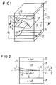
- the first integrated optical waveguide 1 is e.g. a layer waveguide as shown in FIG. 4d in a top view of the end face 11 for coupling in the optical wave with a small spot width.
- the thickness d 1 of the layer 14 of the first waveguide 1 is adapted to the vertical small spot width w 1 of the spot 4 of the optical wave to be coupled.
- the horizontal width of this waveguide is adapted to the horizontal small spot width w 1 'of the spot 4 of the wave to be coupled in and defined by the width d 1' of the rib 10 projecting upward from the layer 14.
- Layer 14 and rib 10 of waveguide 1 consist, for example, of InGaAsP, which has a higher refractive index than the material, for example consisting of InP, in which first waveguide 1 is embedded.
- the waveguiding layer 23 of the second integrated-optical waveguide 2, in which the first waveguide 1 is arranged and which completely comprises this first waveguide 1, consists of this or such a material with a lower refractive index surrounds.
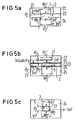
- the second waveguide 2 consists, for example, of the waveguide shown in FIG. 5a in a top view of the end face 21 for coupling out the optical wave with a larger spot width, which consists of the layer 23 of undoped InP arranged between two layers 22 and 24 of n-doped InP.
- the thickness d2 of the layer 23 is adapted to the vertical larger spot width w2 of the spot 5 of the optical wave to be coupled out.
- the horizontal width of this second waveguide 2 is adapted to the horizontal larger spot width w2 'of the spot 5 of the wave to be coupled out and defined by the width d2' of the rib 20 projecting downward from the layer 23.
- the end face 11 for coupling in the optical wave with a smaller spot width of the first waveguide 1 lies in an end face 25 of the second waveguide 2. From this end face 25, the end face 21 for coupling out the optical wave with a larger spot width of the second waveguide 2 is turned away.
- the first waveguide 1 ends at a distance D in front of the end surface 21 for coupling out the optical wave of larger spot width of the second waveguide 2 and tapers from the end surface 11 for coupling in the longitudinal axial direction 31 to the end surface 21 for coupling out, for example in such a way that the first waveguide 1 perpendicular to the horizontal plane of its layer 14 and the layer 23 of the second waveguide 2 becomes continuously or gradually thinner, as shown in FIGS. 1 to 3.
- the plane of the layers 14 and 23 is perpendicular to the plane of the drawing in FIGS. 2 and 3 and contains the longitudinal axis 3 of the first and second waveguides 1 and 2.
- the tapering first waveguide 1 should be as symmetrical as possible to the plane of the layers 14 and 23, as is indicated by the dashed line 6 in FIG. 2.
- a somewhat asymmetrical configuration with respect to this level, in which the tapering first waveguide 1 is formed only on one side of this level, as shown in FIGS. 1 to 3, is in many cases technologically easier to manufacture and in many cases meets the practical requirements. especially when the small spot width w1 is very small compared to the larger spot width w2, for example one or several orders of magnitude smaller than the larger spot width w2. This is the case, for example, when a semiconductor laser diode is to be coupled to an optical fiber, for example a single-mode fiber.
- a widening of the coupled-in and guided wave perpendicular to the axis 3 parallel to the plane of the layers 14 and 23 can be achieved by widening the first waveguide 1 in this direction, it being sufficient in the example according to FIG. 1, the rib 10 in the longitudinal axial direction 31 to widen continuously or stepwise, as shown in FIG. 1.
- the length L of the tapering first waveguide 1 in the longitudinal axial direction 31 should be chosen so that the guided modes are adiabatically converted into one another.
- a tapered waveguide 1 that is too short leads to radiation losses and excitation of higher modes.
- a tapered first waveguide 1 increases the chip area required. A favorable compromise can be made here.
- the embodiment of the first optical waveguide 1 depends on the type of the wave which is to be coupled in Components, for example lasers, amplifiers, filters and / or switches, which can be integrated on a common chip together with the arrangement according to the invention.
- the embodiments of the first waveguide 1 shown in FIGS. 4a to 4c can be used, for example.
- the embodiment according to FIG. 4a differs from that according to FIG. 4d in that there is no layer 13 present in FIG. 4d.
- the width d 1 'of the horizontal spot width w 1' adapted rib 10 of the layer 14 is separated by a layer 13 and consists for example of InP.
- the waveguide 1 is defined solely by a strip-shaped layer 14 of thickness d 1 and width d 1 ', which is completely embedded in a material 12.
- the layer 14 consists of n-doped InP or InGaAsP and the surrounding material 12 consists of InP.
- the embodiment of the second waveguide 2 depends on the component to be coupled to its end face 21, for example a single-mode fiber.
- the geometry of this second waveguide 2 is to be designed in such a way that the guided optical wave is matched as well as possible to the monomode fiber or another component to be coupled.
- FIGS. 5b and 5c further possible embodiments of the second waveguide 2 are shown in FIGS. 5b and 5c.
- the wave-guiding layer 23 is formed by a layer of InP arranged between two relatively thin layers 25 and 26 of InGaAsP the thickness d2 determined.
- the width d2 'of the second waveguide 2 is determined by a further thin layer 27 of InGaAsP of this width d2'.
- This layer 27 is arranged at a distance d3 from the layer 23 and embedded in a layer 23 made of InP, which borders on the layer 25.
- a layer 24 made of InP borders on the layer 26.
- the exemplary embodiment according to FIG. 3 is implemented with a second waveguide 2 according to FIG. 5b, layer 27 not being shown in layer 22 in FIG. 3.
- the embodiment according to FIG. 5c corresponds to the dimensions of the embodiment according to FIG. 4c of the first waveguide 1.
- FIGS. 4a to 4d of the first waveguide 1 and the embodiments according to FIGS. 5a to 5c of the second waveguide 2 can be combined with one another as far as this is compatible with the technological manufacture.
Applications Claiming Priority (2)
| Application Number | Priority Date | Filing Date | Title |
|---|---|---|---|
| DE4100991 | 1991-01-15 | ||
| DE4100991 | 1991-01-15 |
Publications (3)
| Publication Number | Publication Date |
|---|---|
| EP0495202A2 true EP0495202A2 (fr) | 1992-07-22 |
| EP0495202A3 EP0495202A3 (en) | 1992-11-19 |
| EP0495202B1 EP0495202B1 (fr) | 1996-04-24 |
Family
ID=6423054
Family Applications (1)
| Application Number | Title | Priority Date | Filing Date |
|---|---|---|---|
| EP91121196A Expired - Lifetime EP0495202B1 (fr) | 1991-01-15 | 1991-12-10 | Dispositif pour changer une onde optique avec un petit diamètre du mode en une onde avec un diamètre plus grand |
Country Status (4)
| Country | Link |
|---|---|
| US (1) | US5153935A (fr) |
| EP (1) | EP0495202B1 (fr) |
| JP (1) | JP3151274B2 (fr) |
| DE (1) | DE59107727D1 (fr) |
Cited By (5)
| Publication number | Priority date | Publication date | Assignee | Title |
|---|---|---|---|---|
| EP0583679A1 (fr) * | 1992-08-14 | 1994-02-23 | Siemens Aktiengesellschaft | Dispositif pour transformer une onde optique avec une coupe transversale relativement petite en une onde optique avec une coupe transversale plus large |
| WO1994015231A1 (fr) * | 1992-12-29 | 1994-07-07 | Tomas Brenner | Procede de production d'adaptateurs de formes de modes optiques |
| EP0641049A1 (fr) * | 1993-08-31 | 1995-03-01 | Fujitsu Limited | Dispositif optique à semi-conducteur et sa méthode de fabrication |
| EP0498170B1 (fr) * | 1991-02-08 | 1997-08-27 | Siemens Aktiengesellschaft | Composant optique intégré pour accoupler des guides d'ondes de dimensions différentes |
| WO2002088799A1 (fr) * | 2001-04-30 | 2002-11-07 | Fraunhofer-Gesellschaft zur Förderung der angewandten Forschung e.V. | Transformateur du rayon equivalent du faisceau guide a optique integree destine a des adaptations de champ adiabatiques et monomodes |
Families Citing this family (8)
| Publication number | Priority date | Publication date | Assignee | Title |
|---|---|---|---|---|
| FR2730821B1 (fr) * | 1995-02-22 | 1997-04-30 | Alcatel Optronics | Guide optique segmente pouvant notamment etre inclus dans un dispositif semiconducteur |
| US6571039B1 (en) * | 1999-11-23 | 2003-05-27 | Lnl Technologies, Inc. | Optical waveguide having a weakly-confining waveguide section and a strongly-confining waveguide section optically coupled by a tapered neck |
| KR100315419B1 (ko) * | 1999-12-23 | 2001-11-26 | 오길록 | 초고속 폴리머 마하-젠더 광변조기를 위한 진행파형코플라나 전극의 제조 방법 |
| US6963597B2 (en) * | 2000-04-28 | 2005-11-08 | Photodigm, Inc. | Grating-outcoupled surface-emitting lasers |
| US6775454B2 (en) * | 2001-05-14 | 2004-08-10 | Nippon Telegraph And Telephone Corporation | Silica-based optical waveguide circuit and fabrication method thereof |
| GB2388917A (en) * | 2002-05-25 | 2003-11-26 | Bookham Technology Plc | Semiconductor optical waveguide with a varying taper |
| US20050123244A1 (en) * | 2003-12-03 | 2005-06-09 | Block Bruce A. | Embedded optical waveguide coupler |
| JP5370678B2 (ja) * | 2008-01-31 | 2013-12-18 | 日本電気株式会社 | 細線導波路とリッジ導波路とを低損失に接続することができる光結合器 |
Citations (3)
| Publication number | Priority date | Publication date | Assignee | Title |
|---|---|---|---|---|
| JPS61256305A (ja) * | 1985-05-10 | 1986-11-13 | Mitsubishi Electric Corp | 光集積回路 |
| US4773720A (en) * | 1986-06-03 | 1988-09-27 | General Electric Company | Optical waveguide |
| EP0356872A2 (fr) * | 1988-08-25 | 1990-03-07 | Alcatel SEL Aktiengesellschaft | Méthode pour changer le diamètre du mode d'une fibre monomode à saut d'indice |
Family Cites Families (4)
| Publication number | Priority date | Publication date | Assignee | Title |
|---|---|---|---|---|
| GB2152694B (en) * | 1984-01-05 | 1987-06-24 | Standard Telephones Cables Ltd | Wavelength selective optical waveguide coupler |
| US4669815A (en) * | 1985-08-12 | 1987-06-02 | Trw Inc. | Integrated optical waveguide multiplexer/demultiplexer |
| US4796975A (en) * | 1987-05-14 | 1989-01-10 | Amphenol Corporation | Method of aligning and attaching optical fibers to substrate optical waveguides and substrate optical waveguide having fibers attached thereto |
| US5062681A (en) * | 1990-05-02 | 1991-11-05 | E. I. Du Pont De Nemours And Company | Slot-coupling of optical waveguide to optical waveguide devices |
-
1991
- 1991-12-10 DE DE59107727T patent/DE59107727D1/de not_active Expired - Lifetime
- 1991-12-10 EP EP91121196A patent/EP0495202B1/fr not_active Expired - Lifetime
- 1991-12-13 US US07/806,352 patent/US5153935A/en not_active Expired - Lifetime
-
1992
- 1992-01-13 JP JP02480292A patent/JP3151274B2/ja not_active Expired - Lifetime
Patent Citations (3)
| Publication number | Priority date | Publication date | Assignee | Title |
|---|---|---|---|---|
| JPS61256305A (ja) * | 1985-05-10 | 1986-11-13 | Mitsubishi Electric Corp | 光集積回路 |
| US4773720A (en) * | 1986-06-03 | 1988-09-27 | General Electric Company | Optical waveguide |
| EP0356872A2 (fr) * | 1988-08-25 | 1990-03-07 | Alcatel SEL Aktiengesellschaft | Méthode pour changer le diamètre du mode d'une fibre monomode à saut d'indice |
Non-Patent Citations (2)
| Title |
|---|
| APPLIED PHYSICS LETTERS. Bd. 55, Nr. 23, 4. Dezember 1989, NEW YORK US Seiten 2389 - 2391 Y. SHANI ET AL. 'Efficient coupling of a semiconductor laser to an optical fiber by means of a tapered waveguide on silicon' * |
| PATENT ABSTRACTS OF JAPAN vol. 11, no. 109 (P-564)(2556) 7. März 1987 & JP-A-61 256 305 ( MITSUBISHI ELECTRIC ) * |
Cited By (7)
| Publication number | Priority date | Publication date | Assignee | Title |
|---|---|---|---|---|
| EP0498170B1 (fr) * | 1991-02-08 | 1997-08-27 | Siemens Aktiengesellschaft | Composant optique intégré pour accoupler des guides d'ondes de dimensions différentes |
| EP0583679A1 (fr) * | 1992-08-14 | 1994-02-23 | Siemens Aktiengesellschaft | Dispositif pour transformer une onde optique avec une coupe transversale relativement petite en une onde optique avec une coupe transversale plus large |
| WO1994015231A1 (fr) * | 1992-12-29 | 1994-07-07 | Tomas Brenner | Procede de production d'adaptateurs de formes de modes optiques |
| EP0641049A1 (fr) * | 1993-08-31 | 1995-03-01 | Fujitsu Limited | Dispositif optique à semi-conducteur et sa méthode de fabrication |
| US5987046A (en) * | 1993-08-31 | 1999-11-16 | Fujitsu Limited | Optical semiconductor device and a method of manufacturing the same |
| US6238943B1 (en) | 1993-08-31 | 2001-05-29 | Fujitsu Limited | Optical semiconductor device and a method of manufacturing the same |
| WO2002088799A1 (fr) * | 2001-04-30 | 2002-11-07 | Fraunhofer-Gesellschaft zur Förderung der angewandten Forschung e.V. | Transformateur du rayon equivalent du faisceau guide a optique integree destine a des adaptations de champ adiabatiques et monomodes |
Also Published As
| Publication number | Publication date |
|---|---|
| JPH04360105A (ja) | 1992-12-14 |
| EP0495202A3 (en) | 1992-11-19 |
| EP0495202B1 (fr) | 1996-04-24 |
| DE59107727D1 (de) | 1996-05-30 |
| US5153935A (en) | 1992-10-06 |
| JP3151274B2 (ja) | 2001-04-03 |
Similar Documents
| Publication | Publication Date | Title |
|---|---|---|
| EP0890121B1 (fr) | Transformateurs optiques integres de l'etalement du faisceau | |
| EP0498170B1 (fr) | Composant optique intégré pour accoupler des guides d'ondes de dimensions différentes | |
| EP0037057B1 (fr) | Branchement de guides d'ondes optiquesà faibles effets de polarisation | |
| EP0012189B1 (fr) | Elément coupleur pour dériver une fraction de lumière d'un guide d'ondes optique comprenant une fibre entourée d'une gaine | |
| EP0495202B1 (fr) | Dispositif pour changer une onde optique avec un petit diamètre du mode en une onde avec un diamètre plus grand | |
| DE2750322B2 (de) | Optische Vorrichtung zur Einkopplung der aus einem Halbleiterlaser austretenden Strahlung in eine optische Faser | |
| EP0831344B1 (fr) | Arrangement de deux guides d'ondes en optique integré à la surface d'un substrat | |
| DE19711507A1 (de) | Optische Verzweigungs-/Kreuzungs-Wellenleiterschaltung | |
| EP0583679B1 (fr) | Dispositif d'optique intégrée pour transformer une onde optique avec une coupe transversale relativement petite en une onde optique avec une coupe transversale plus large | |
| EP0361153A2 (fr) | Dispositif pour coupler une fibre optique à une fenêtre de couplage d'un élément optique à intégration plane et sa méthode de fabrication | |
| EP0107840B1 (fr) | Procédé de fabrication d'un coupleur optique, en particulier procédé pour diminuer l'épaisseur de la gaine en quartz d'une fibre optique en verre | |
| DE2905916A1 (de) | Faseroptische uebertragungsvorrichtung | |
| EP0048855A2 (fr) | Elément de réglage de la transmission de lumière entre des guides d'ondes optiques | |
| EP3545347B1 (fr) | Composant optoélectronique et procédé de fabrication d'un composant optoélectronique | |
| WO1998000894A2 (fr) | Composant semi-conducteur optique a guide d'ondes nervure profond | |
| EP0660143A2 (fr) | Dispositif de couplage entre une fibre optique et un guide d'onde optique | |
| EP0589902A1 (fr) | Circuit optique integre. | |
| DE4244268A1 (de) | Hochauflösendes optisches System mit einer Tastspitze | |
| EP0477604A2 (fr) | Coupleur optique directionnel intégré, commandable | |
| DE2851654C2 (fr) | ||
| DE60218325T2 (de) | Optischer filter | |
| DE2927025C2 (fr) | ||
| EP0737872A2 (fr) | Dispositif de branchement optique | |
| EP0482308B1 (fr) | Composant flexible optique | |
| EP0498320A1 (fr) | Transition de guides d'ondes lumineuses |
Legal Events
| Date | Code | Title | Description |
|---|---|---|---|
| PUAI | Public reference made under article 153(3) epc to a published international application that has entered the european phase |
Free format text: ORIGINAL CODE: 0009012 |
|
| AK | Designated contracting states |
Kind code of ref document: A2 Designated state(s): DE FR GB IT |
|
| PUAL | Search report despatched |
Free format text: ORIGINAL CODE: 0009013 |
|
| AK | Designated contracting states |
Kind code of ref document: A3 Designated state(s): DE FR GB IT |
|
| 17P | Request for examination filed |
Effective date: 19930507 |
|
| 17Q | First examination report despatched |
Effective date: 19950407 |
|
| GRAH | Despatch of communication of intention to grant a patent |
Free format text: ORIGINAL CODE: EPIDOS IGRA |
|
| GRAA | (expected) grant |
Free format text: ORIGINAL CODE: 0009210 |
|
| AK | Designated contracting states |
Kind code of ref document: B1 Designated state(s): DE FR GB IT |
|
| REF | Corresponds to: |
Ref document number: 59107727 Country of ref document: DE Date of ref document: 19960530 |
|
| ET | Fr: translation filed | ||
| ITF | It: translation for a ep patent filed |
Owner name: STUDIO JAUMANN |
|
| GBT | Gb: translation of ep patent filed (gb section 77(6)(a)/1977) |
Effective date: 19960627 |
|
| PLBE | No opposition filed within time limit |
Free format text: ORIGINAL CODE: 0009261 |
|
| STAA | Information on the status of an ep patent application or granted ep patent |
Free format text: STATUS: NO OPPOSITION FILED WITHIN TIME LIMIT |
|
| 26N | No opposition filed | ||
| REG | Reference to a national code |
Ref country code: GB Ref legal event code: IF02 |
|
| PG25 | Lapsed in a contracting state [announced via postgrant information from national office to epo] |
Ref country code: IT Free format text: LAPSE BECAUSE OF NON-PAYMENT OF DUE FEES Effective date: 20051210 |
|
| PGFP | Annual fee paid to national office [announced via postgrant information from national office to epo] |
Ref country code: FR Payment date: 20101230 Year of fee payment: 20 |
|
| PGFP | Annual fee paid to national office [announced via postgrant information from national office to epo] |
Ref country code: GB Payment date: 20101209 Year of fee payment: 20 |
|
| PGFP | Annual fee paid to national office [announced via postgrant information from national office to epo] |
Ref country code: DE Payment date: 20110221 Year of fee payment: 20 |
|
| REG | Reference to a national code |
Ref country code: DE Ref legal event code: R071 Ref document number: 59107727 Country of ref document: DE |
|
| REG | Reference to a national code |
Ref country code: DE Ref legal event code: R071 Ref document number: 59107727 Country of ref document: DE |
|
| REG | Reference to a national code |
Ref country code: GB Ref legal event code: PE20 Expiry date: 20111209 |
|
| PG25 | Lapsed in a contracting state [announced via postgrant information from national office to epo] |
Ref country code: GB Free format text: LAPSE BECAUSE OF EXPIRATION OF PROTECTION Effective date: 20111209 |
|
| PG25 | Lapsed in a contracting state [announced via postgrant information from national office to epo] |
Ref country code: DE Free format text: LAPSE BECAUSE OF EXPIRATION OF PROTECTION Effective date: 20111211 |