EP0490880A2 - Negative feedback power supply apparatus - Google Patents
Negative feedback power supply apparatus Download PDFInfo
- Publication number
- EP0490880A2 EP0490880A2 EP92103646A EP92103646A EP0490880A2 EP 0490880 A2 EP0490880 A2 EP 0490880A2 EP 92103646 A EP92103646 A EP 92103646A EP 92103646 A EP92103646 A EP 92103646A EP 0490880 A2 EP0490880 A2 EP 0490880A2
- Authority
- EP
- European Patent Office
- Prior art keywords
- voltage
- core
- load
- power supply
- circuit
- Prior art date
- Legal status (The legal status is an assumption and is not a legal conclusion. Google has not performed a legal analysis and makes no representation as to the accuracy of the status listed.)
- Granted
Links
Images


Classifications
-
- H—ELECTRICITY
- H02—GENERATION; CONVERSION OR DISTRIBUTION OF ELECTRIC POWER
- H02M—APPARATUS FOR CONVERSION BETWEEN AC AND AC, BETWEEN AC AND DC, OR BETWEEN DC AND DC, AND FOR USE WITH MAINS OR SIMILAR POWER SUPPLY SYSTEMS; CONVERSION OF DC OR AC INPUT POWER INTO SURGE OUTPUT POWER; CONTROL OR REGULATION THEREOF
- H02M1/00—Details of apparatus for conversion
- H02M1/20—Contact mechanisms of dynamic converters
- H02M1/24—Contact mechanisms of dynamic converters incorporating rolling or tumbling contacts
-
- G—PHYSICS
- G01—MEASURING; TESTING
- G01R—MEASURING ELECTRIC VARIABLES; MEASURING MAGNETIC VARIABLES
- G01R31/00—Arrangements for testing electric properties; Arrangements for locating electric faults; Arrangements for electrical testing characterised by what is being tested not provided for elsewhere
- G01R31/40—Testing power supplies
- G01R31/42—AC power supplies
-
- G—PHYSICS
- G01—MEASURING; TESTING
- G01R—MEASURING ELECTRIC VARIABLES; MEASURING MAGNETIC VARIABLES
- G01R35/00—Testing or calibrating of apparatus covered by the other groups of this subclass
- G01R35/02—Testing or calibrating of apparatus covered by the other groups of this subclass of auxiliary devices, e.g. of instrument transformers according to prescribed transformation ratio, phase angle, or wattage rating
-
- G—PHYSICS
- G05—CONTROLLING; REGULATING
- G05F—SYSTEMS FOR REGULATING ELECTRIC OR MAGNETIC VARIABLES
- G05F1/00—Automatic systems in which deviations of an electric quantity from one or more predetermined values are detected at the output of the system and fed back to a device within the system to restore the detected quantity to its predetermined value or values, i.e. retroactive systems
- G05F1/10—Regulating voltage or current
- G05F1/12—Regulating voltage or current wherein the variable actually regulated by the final control device is ac
- G05F1/32—Regulating voltage or current wherein the variable actually regulated by the final control device is ac using magnetic devices having a controllable degree of saturation as final control devices
- G05F1/34—Regulating voltage or current wherein the variable actually regulated by the final control device is ac using magnetic devices having a controllable degree of saturation as final control devices combined with discharge tubes or semiconductor devices
- G05F1/38—Regulating voltage or current wherein the variable actually regulated by the final control device is ac using magnetic devices having a controllable degree of saturation as final control devices combined with discharge tubes or semiconductor devices semiconductor devices only
-
- H—ELECTRICITY
- H02—GENERATION; CONVERSION OR DISTRIBUTION OF ELECTRIC POWER
- H02M—APPARATUS FOR CONVERSION BETWEEN AC AND AC, BETWEEN AC AND DC, OR BETWEEN DC AND DC, AND FOR USE WITH MAINS OR SIMILAR POWER SUPPLY SYSTEMS; CONVERSION OF DC OR AC INPUT POWER INTO SURGE OUTPUT POWER; CONTROL OR REGULATION THEREOF
- H02M1/00—Details of apparatus for conversion
Definitions
- the present invention relates to a negative feedback power supply apparatus for a load.
- the present invention is applied to an apparatus for testing the AC magnetization characteristics of a toroidal core or a cut-core type core, a power supply apparatus for a load of a rectifier circuit, or a power supply apparatus for a load for a distorted current.
- a prior art testing apparatus for a toroidal core having primary and secondary windings an input AC power supply and an AC current meter are connected to the primary winding, and an AC voltage meter is connected to the secondary winding. Further, a power meter is connected between the primary winding and the secondary winding.
- a measurement of a primary current I P and a measurement of a core loss are carried out at the periphery of a saturated magnetic flux, which is one of the AC magnetization characteristics to be tested. Note that the measurement of core loss is made by the power meter.
- an object of the present invention is to provide a power supply apparatus for testing a core, whereby a winding operation using connector-type contacts is unnecessary, an adjustment of an input voltage for every core is unnecessary even when the DC resistance and the equivalent AC and DC resistances of the primary winding are changed by the contacts, and no distortion is generated in the magnetic flux density of the core, thereby enabling a correct and stable measurement.
- Another object of the present invention is to provide a power supply apparatus for a load such as a load of a rectifier circuit and a distortion current load.
- a suggested power supply apparatus for a toroidal core i.e., a suggested apparatus for testing a toroidal core
- test windings W 1 and W 2 may be wound on the core 1.
- connector-type contacts CW 1 and CW 2 are provided to reduce the desorption of the windings W 1 and W 2 .
- a current flowing therethrough is small and the reduction in potential and heat generation by the resistance component of the windings is also small.
- FIG. 2 a testing apparatus for the toroidal core 1 having the test windings W 1 and W 2 are illustrated.
- reference numeral 2 designates an input AC power supply, 3 an AC current meter, 4 an AC voltage meter, P 1 and P 2 terminals for the connection of the primary winding W 1 , and S 1 and S 2 terminals for the connection of the secondary winding W 2 .
- a measurement of a primary current I P and a measurement of core loss are carried out at the periphery of a saturated magnetic flux of the core 1, which is one of the tests of AC magnetization characteristics. Note that the measurement of core loss is made by a power meter W.
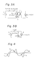
- FIG. 3A an equivalent circuit thereof is illustrated in Fig. 3A
- a simplified equivalent circuit is illustrated in Fig. 3B.
- the power meter W is omitted from Figs. 3A and 3B.
- reference T designates an ideal transformer
- Rp an equivalent DC resistance of the primary winding W 1
- R c an equivalent contact DC resistance of the connector contact CW 1
- R z p an equivalent AC resistance of the primary winding W 1
- the resistances of the secondary winding W 2 and the contact CW 2 are negligible.
- the equivalent DC resistance Rp and the equivalent DC resistance R c are unstable.
- the resistance Rp fluctuates from 1 to 1.2 Q due to the generation of heat by the exciting current I P
- the contact DC resistance R c fluctuates from 0 to 0.8 ⁇ due to the state of the contact CW 1 .
- the equivalent AC resistance R z p fluctuates from ⁇ to 0.5 ⁇ due to the saturation characteristics of the core 1.
- the distortion of the magnetic flux waveform i.e., the distortion of the output voltage E s
- the peak current portion of the exciting current I P is suppressed. Therefore, it is impossible to carry out a correct measurement.
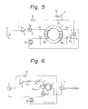
- Fig. 5 which illustrates a first embodiment of the present invention applied to a testing apparatus for a toroidal core
- an analog negative feedback loop circuit is added to the elements of Fig. 2. That is, an amplifier 5, a feedback resistor 6, and a phase adjusting circuit 7 formed by a capacitor 71 and a resistor 72 are added to the elements of Fig. 2.
- Fig. 6 is an equivalent circuit diagram of the apparatus of Fig. 5.
- the feedback ratio F is made 0.99 by the feedback resistor 6, the output voltage E s can be represented by where E 1 is the output voltage of the AC power supply 2 and is, in this case, 1 V. Therefore, the maximum of the output voltage E s and the minimum of the output voltage E s
- the fluctuation of the output voltage E s is reduced compared with the case of Fig. 3A (Fig. 3B). Therefore, even when the DC resistance by the contacts, and the equivalent AC and DC resistances of the primary winding W 1 are fluctuated, a substantial adjustment of the input voltage is unnecessary, and as a result, the distortion of the magnetic flux waveform in the core 1, i.e., the distortion of the output voltage E s , is reduced.
- the amplification factor of the amplifier 5 is increased to increase the feedback factor F, the stability of the output voltage E s can be improved.
- an oscillation phenomenon may occur due to the leak reactances of the windings. Such an oscillation phenomenon can be suppressed by adjusting the resistor 71 and/or the capacitor 72 of the phase adjusting circuit 7, to a certain extent.
- phase shift amount is commonly generated by the capacitance component in the negative feedback loop circuit in a relatively high frequency region, and in addition, it is difficult to completely adjust such a phase shift amount by the phase adjusting circuit 7. It is also difficult to adjust this phase shift amount when an inductance component due to the windings and the leak inductances therebetween is added to the negative feedback loop circuit.
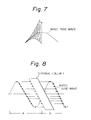
- the output voltage E s of the secondary winding W 2 is still distorted and unstable. That is, in the circuit of Fig. 5, after the oscillation conditions are satisfied in the analog negative feedback loop circuit, a positive feedback control at a specific frequency of about 10 KHz to 1 MHz is triggered by differential noise or the like, and as a result, the amplitude of the input voltage applied to the core 1 is rapidly increased as illustrated in Fig. 7.
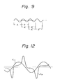
- a waveform to be negatively fed back is stored and is delayed by one cycle of a basic sine-wave, and thereafter, a negative feedback control is carried out by using the delayed waveform. That is, as illustrated in Fig. 8, a voltage error between an input sine-wave voltage and an output voltage is stored and delayed for a period A, and the input sine-wave voltage is corrected by the delayed voltage error for a period B. Therefore, as illustrated in Fig. 9, even when a phase shift amount in the negative feedback loop circuit is larger than 180°, a positive feedback phenomenon is split for every cycle of the basic sine-wave form, so that oscillation is not generated.
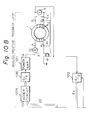
- Fig. 10 which illustrates a second embodiment of the present invention realizing the principle of Figs. 8 and 9, which is also applied to an apparatus for testing a toroidal core.
- a digital negative feedback loop circuit is provided. That is, reference numeral 1001 designates a control portion (CPU); 1002 a frequency switch; 1003 a voltage set switch formed by digital switches; 1004 a basic sine-wave generating circuit (ROM) for generating a sine-wave voltage Eo; and 1005 a voltage adjusting circuit (multiplier) for adjusting the output of the basic sine-wave generating circuit 1004.
- CPU control portion
- 1002 a frequency switch
- 1003 a voltage set switch formed by digital switches
- 1004 a basic sine-wave generating circuit (ROM) for generating a sine-wave voltage Eo
- 1005 a voltage adjusting circuit (multiplier) for adjusting the output of the basic sine-wave generating circuit 1004.
- the frequency of the basic sine-wave voltage Eo of the basic sine-wave generating circuit 1004 is changed by the control portion 1001 in accordance with the state of the frequency switch 1002. That is, the control portion 1001 generates a clock signal having a frequency in accordance with the state of the frequency switch 1002 and transmits this clock to the basic sine-wave generating circuit 1004. Also, the control portion 1001 generates a voltage factor a in accordance with the output of the voltage set switch 1003. As a result, the voltage adjusting circuit 1005 multiplies each digital value of the basic sine-wave voltage Eo by the voltage factor a to generate a new basic sine-wave voltage Eo'.
- Reference numerals 1006 and 1007 designate delay memories for adjusting a total delay time corresponding to one cycle of the basic sine-wave voltage Eo (Eo').Each of the delay memories 1006 and 1007 may be constructed by a bidirectional memory in which a write operation and a read operation can be simultaneously carried out. That is, the delay memories 1006 and 1007 are associated with address counters 1006a and 1007a, respectively, and therefore, the delay memories 1006 and 1007 are operated by write addresses WA and read addresses RA of the address counters 1006 and 1007, which are counted up by clock signals of the control portion 1001. In this case, the delay time period of the delay memory 1006 (1007) is determined by where
- a subtraction circuit 1008 calculates a digital voltage error AE between the basic sine-wave voltage Eo' and an analog/digital (A/D) converted output voltage E s from the ends of the secondary winding W 2 via an A/D converter 1012. Also, an adder circuit 1009 adds the delayed voltage error AE to the basic sine-wave voltage Eo'.
- a D/A converter 1010 performs a D/A conversion upon the output of the adder circuit 1010, and as a result, a power amplifier 1011 supplies an input current I P to the primary winding W 1 in accordance with the analog voltage of the D/A converter 1010.
- the output voltage E s of the secondary winding W 2 is negatively fed back by the digital negative feedback loop circuit formed by the elements 1006, 1008, 1007, and 1012.
- a waveform to be fed back is delayed for one cycle of the basic sine-wave voltage Eo.
- the output voltage E s is stable, as illustrated in Fig. 12, even when the magnetic flux density of the core 1 is extremely large.
- a delay memory 1101, an address counter 1101 a, and an adder circuit 1102 are added to the elements of Fig. 10.
- the three delay memories 1006, 1007, and 1101 adjust a total delay time period corresponding to one cycle of the basic sine-wave voltage Eo (Eo'). Therefore, in Fig. 11, the voltage error AE' to be fed back is summed and added to the basic sine-wave voltage Eo', thereby remarkably increasing the feedback factor F. For example, if the feedback factor F for the first cycle is 0.9, the feedback factor F for the second cycle is 0.99. Also, the feedback factor F for the third cycle, the fourth cycle, ... is 0.999, 0.9999, ....
- Figs. 10 and 11 can be combined with the first embodiment of Fig. 5. That is, an analog negative feedback loop circuit formed by the elements 6 and 7 of Fig. 5 is added to the circuit of Fig. 10 or 11, as indicated by dotted lines.
- the power amplifier 1011 also serves as the differential amplifier 5 of Fig. 5. As a result, it is possible to completely correct the output voltage E s at an even higher speed.
- the primary winding W 1 and the secondary winding W 2 can be of a type other than the connector-type. Also, it is possible to carry out a highly accurate and stable testing (measurement) even when the number of turns of the windings is 1. Also, the arrangement and installation of the contacts CW 1 and CW 2 can be freely determined. Further, the number of turns of the primary winding W 1 need not be the same as that of the secondary winding W 2 .
- the present invention can be applied to an apparatus for testing a separate-type core, and the present invention can be still applied to other power supply apparatuses such as a power supply apparatus for a load of a rectifier circuit, or a power supply apparatus for a distorted current load.
- a winding operation for each core is unnecessary, and a correct and stable test (measurement) can be carried out without adjusting the input voltage, even when the magnetic flux density of a core is extremely large.
Abstract
Description
- The present invention relates to a negative feedback power supply apparatus for a load. For example, the present invention is applied to an apparatus for testing the AC magnetization characteristics of a toroidal core or a cut-core type core, a power supply apparatus for a load of a rectifier circuit, or a power supply apparatus for a load for a distorted current.
- In order to carry out a testing of the AC magnetization characteristics of a large number of toroidal cores, such as exciting currents, and a core loss such as a vortex current loss and a hysteresis loss, it is necessary to wind windings on a core for every test. To simplying this winding operation, connector-type contacts may be used to reduce the desorption of the windings. However, in the actual design of transformers or the like, since the thickness of the windings is as large as possible, to reduce the resistance value thereof, and the number of turns of the windings is large, a current flowing therethrough is small and the reduction in potential and heat generation by the resistance component of the windings is also small. Contrary to this, when the connector-type contacts are used, since the space for installing the connector-shaped contacts is restricted, the thickness of the windings is small and the number of turns of the windings is small. As a result, it is necessary to increase a test exciting current supplied to the primary winding, but such a current is affected by the resistances of the windings and the contacts.
- In a prior art testing apparatus for a toroidal core having primary and secondary windings, an input AC power supply and an AC current meter are connected to the primary winding, and an AC voltage meter is connected to the secondary winding. Further, a power meter is connected between the primary winding and the secondary winding. In this apparatus, a measurement of a primary current IP and a measurement of a core loss are carried out at the periphery of a saturated magnetic flux, which is one of the AC magnetization characteristics to be tested. Note that the measurement of core loss is made by the power meter.
- However, fluctuation of the equivalent DC resistance of the primary winding is caused by the heat generated by the exciting current, and fluctuation of the contact DC resistance of a connector-type contact is caused by the state of the contact. Further, fluctuation of the equivalent AC resistance of the primary winding is caused by the saturation characteristics of the core. Therefore, a large fluctuation occurs in the output voltage of the secondary winding. Further, at the periphery of a saturated magnetic flux density, an extraordinary current generated locally at one cycle of the AC current invites a spontaneous reduction in the equivalent AC resistance, and as a result, the waveform of the output voltage generated at the secondary winding is greatly distorted. This large fluctuation and distortion lead to the generation of a large fluctuation and distortion in the magnetic flux density of the core, which is very disadvantageous from the viewpoint of obtaining a definite AC magnetic flux density. Accordingly, to make the output voltage of the secondary winding constant, even when the voltage of the AC power supply is adjusted so as to correct the output voltage generated in the secondary winding W2 , the distortion of the magnetic flux density waveform, i.e., the distortion of the output voltage, remains and, simultaneously, the peak current portion of the exciting current is suppressed. Therefore, it is impossible to carry out a correct measurement.
- Therefore, an object of the present invention is to provide a power supply apparatus for testing a core, whereby a winding operation using connector-type contacts is unnecessary, an adjustment of an input voltage for every core is unnecessary even when the DC resistance and the equivalent AC and DC resistances of the primary winding are changed by the contacts, and no distortion is generated in the magnetic flux density of the core, thereby enabling a correct and stable measurement.
- Another object of the present invention is to provide a power supply apparatus for a load such as a load of a rectifier circuit and a distortion current load.
- The present invention will be more clearly understood from the description as set forth below with reference to the accompanying drawings, wherein:
- Fig. 1 is a diagram showing suggested examples of tests of windings;
- Fig. 2 is a circuit diagram illustrating a suggested apparatus for testing a toroidal core;
- Figs. 3A and 3B are equivalent circuit diagrams of the apparatus of Fig. 2;
- Fig. 4 is a diagram showing the output characteristics of the apparatus of Fig. 2;
- Fig. 5 is a circuit diagram illustrating a first embodiment of the power supply apparatus according to the present invention;
- Fig. 6 is an equivalent circuit diagram of the apparatus of Fig. 5;
- Fig. 7 is a diagram showing an oscillation phenomenon generated in the apparatus of Fig. 5;
- Figs. 8 and 9 are timing diagrams schematically explaining a basic principle of the present invention;
- Figs. 10 and 11 are circuit diagrams illustrating second and third embodiments, respectively, of the power supply apparatus according to the present invention; and
- Fig. 12 is a diagram showing the output characteristics of the apparatuses of Figs. 10 and 11.
- First, a suggested power supply apparatus for a toroidal core, i.e., a suggested apparatus for testing a toroidal core, will be explained.
- As illustrated in Fig. 1, to test a
toroidal core 1, test windings W1 and W2 may be wound on thecore 1. In this case, in order to simplify the winding operation, connector-type contacts CW1 and CW2 are provided to reduce the desorption of the windings W1 and W2. In an actual design of transformers and the like, since the thickness of the windings is as large as possible, to reduce the resistance value thereof, and the number of turns of windings is as large as possible, a current flowing therethrough is small and the reduction in potential and heat generation by the resistance component of the windings is also small. In Fig. 1, however, since the space for installing the connector-type contacts CW1 and CW2 is restricted, the thickness of the windings is small and the number of turns of the windings is small. As a result, it is necessary to increase an exciting current or testing supplied to the primary winding W1, and in addition, such a current is affected by the resistances of the windings W1 and W2 and the contacts CW1 and CW2. In Fig. 1, note that upper and lower contacts of the connector-type connectors CW1 and CW2 are separated from each other when thecore 1 is inserted thereinto, and are connected when a testing (measuring) operation is carried out, and thus a winding operation of the windings W1 and W2 is unnecessary. - In Fig. 2, a testing apparatus for the
toroidal core 1 having the test windings W1 and W2 are illustrated. In Fig. 2,reference numeral 2 designates an input AC power supply, 3 an AC current meter, 4 an AC voltage meter, P1 and P2 terminals for the connection of the primary winding W1, and S1 and S2 terminals for the connection of the secondary winding W2. According to this circuit, a measurement of a primary current IP and a measurement of core loss are carried out at the periphery of a saturated magnetic flux of thecore 1, which is one of the tests of AC magnetization characteristics. Note that the measurement of core loss is made by a power meter W. - In order to easily understand the circuit of Fig. 2, an equivalent circuit thereof is illustrated in Fig. 3A, and a simplified equivalent circuit is illustrated in Fig. 3B. Note that the power meter W is omitted from Figs. 3A and 3B. In Fig. 3A, reference T designates an ideal transformer, Rp an equivalent DC resistance of the primary winding W1, Rc an equivalent contact DC resistance of the connector contact CW1, and Rzp an equivalent AC resistance of the primary winding W1. Note that the resistances of the secondary winding W2 and the contact CW2 are negligible. For example, the equivalent DC resistance Rp and the equivalent DC resistance Rc are unstable. That is, the resistance Rp fluctuates from 1 to 1.2 Q due to the generation of heat by the exciting current IP , and the contact DC resistance Rc fluctuates from 0 to 0.8 Ω due to the state of the contact CW1. Also, the equivalent AC resistance Rzp fluctuates from ∞ to 0.5 Ω due to the saturation characteristics of the
core 1. Therefore, if the voltage of theAC power supply 2 is 1 V, and an exciting current IP is supplied to the primary winding W1, the output voltage Es of the secondary winding W2 is 1 V where Rp = 1 Q, Rc = 0 Q and Rzp = ∞ Q, and 0.2 V where Rp = 1.2 Q, Rc = 0.8 Q, and Rzp = 0.5 Q, which means that the fluctuation of the output voltage Es is large. Further, at the periphery of a saturated magnetic flux density of thecore 1, an extraordinary current generated locally at one cycle of the AC current invites a spontaneous reduction in the equivalent AC resistance Rzp , and as a result, the waveform of the output voltage Es generated at the secondary winding W2 is greatly distorted. This large fluctuation and distortion leads to the generation of a large fluctuation and distortion in the magnetic flux of thecore 1, which is very disadvantageous in view of the need to obtain a definite AC magnetic flux. Accordingly, to make the output voltage Es constant, when the voltage of theAC power supply 1 is adjusted so as to correct the voltage Es generated in the secondary winding W2 , the distortion of the magnetic flux waveform, i.e., the distortion of the output voltage Es , remains as illustrated in Fig. 4, and simultaneously, the peak current portion of the exciting current IP is suppressed. Therefore, it is impossible to carry out a correct measurement. - In Fig. 5, which illustrates a first embodiment of the present invention applied to a testing apparatus for a toroidal core, an analog negative feedback loop circuit is added to the elements of Fig. 2. That is, an
amplifier 5, afeedback resistor 6, and aphase adjusting circuit 7 formed by acapacitor 71 and aresistor 72 are added to the elements of Fig. 2. Note that Fig. 6 is an equivalent circuit diagram of the apparatus of Fig. 5. - Here, assume that there is no negative feedback circuit, the amplification factor F of the
amplifier 5 having anoutput impedance 0 is 100, and the voltage of theAC power supply 2 is 1 V x 1/100 = 0.01 V. Then, the circuit of Fig. 5 is substantially the same as that of Fig. 2, and therefore, if the values of the equivalent DC resistance Rp , the equivalent contact resistance Rα , and the equivalent AC resistance Rzp are the same as in Fig. 3A, the output voltage Es is also changed from 1 to 0.2 V. That is, if a total amplification factor A' is determined by the ratio of the input voltage (= 0.01 V) of theAC power supply 2 to the output voltage Es , the factor A' is fluctuated by
- Next, consider the presence of the negative feedback circuit according to the present invention. Here, the feedback ratio F is made 0.99 by the
feedback resistor 6, the output voltage Es can be represented by
where E1 is the output voltage of theAC power supply 2 and is, in this case, 1 V. Therefore, the maximum of the output voltage Es
and the minimum of the output voltage Es
- Thus, the fluctuation of the output voltage Es is reduced compared with the case of Fig. 3A (Fig. 3B). Therefore, even when the DC resistance by the contacts, and the equivalent AC and DC resistances of the primary winding W1 are fluctuated, a substantial adjustment of the input voltage is unnecessary, and as a result, the distortion of the magnetic flux waveform in the
core 1, i.e., the distortion of the output voltage Es , is reduced. Note that, if the amplification factor of theamplifier 5 is increased to increase the feedback factor F, the stability of the output voltage Es can be improved. However, when the feedback factor F is increased, an oscillation phenomenon may occur due to the leak reactances of the windings. Such an oscillation phenomenon can be suppressed by adjusting theresistor 71 and/or thecapacitor 72 of thephase adjusting circuit 7, to a certain extent. - In the circuit of Fig. 5 having an analog negative feedback circuit, an accurate measurement can be obtained for a directional silicon steel core having a magnetic flux density of about 17000 gauss. Also, when an extremely distorted exciting current IP is supplied to the primary winding W1 thereby generating a saturated magnetic flux density of about 18000 to 20000 gauss in the
core 1, both the feedback factor F and the amplification factor A' must be increased to obtain a highly accurate and stable measurement. In this case, however, an oscillation phenomenon always occurs. That is, when the amplification factor A' is larger than 1 and a phase shift amount in the negative feedback loop circuit is larger than 180°, the oscillation conditions may be satisfied. Such a phase shift amount is commonly generated by the capacitance component in the negative feedback loop circuit in a relatively high frequency region, and in addition, it is difficult to completely adjust such a phase shift amount by thephase adjusting circuit 7. It is also difficult to adjust this phase shift amount when an inductance component due to the windings and the leak inductances therebetween is added to the negative feedback loop circuit. - Thus, in the
core 1 having a relatively high magnetic flux density, even if an analog negative feedback loop circuit is used, the output voltage Es of the secondary winding W2 is still distorted and unstable. That is, in the circuit of Fig. 5, after the oscillation conditions are satisfied in the analog negative feedback loop circuit, a positive feedback control at a specific frequency of about 10 KHz to 1 MHz is triggered by differential noise or the like, and as a result, the amplitude of the input voltage applied to thecore 1 is rapidly increased as illustrated in Fig. 7. - In Figs. 8 and 9, which show a digital negative feedback control according to the present invention, to prevent the generation of a positive feedback phenomenon in the negative feedback loop circuit, a waveform to be negatively fed back is stored and is delayed by one cycle of a basic sine-wave, and thereafter, a negative feedback control is carried out by using the delayed waveform. That is, as illustrated in Fig. 8, a voltage error between an input sine-wave voltage and an output voltage is stored and delayed for a period A, and the input sine-wave voltage is corrected by the delayed voltage error for a period B. Therefore, as illustrated in Fig. 9, even when a phase shift amount in the negative feedback loop circuit is larger than 180°, a positive feedback phenomenon is split for every cycle of the basic sine-wave form, so that oscillation is not generated.
- In Fig. 10, which illustrates a second embodiment of the present invention realizing the principle of Figs. 8 and 9, which is also applied to an apparatus for testing a toroidal core. In Fig. 10, a digital negative feedback loop circuit is provided. That is,
reference numeral 1001 designates a control portion (CPU); 1002 a frequency switch; 1003 a voltage set switch formed by digital switches; 1004 a basic sine-wave generating circuit (ROM) for generating a sine-wave voltage Eo; and 1005 a voltage adjusting circuit (multiplier) for adjusting the output of the basic sine-wave generating circuit 1004. In this case, the frequency of the basic sine-wave voltage Eo of the basic sine-wave generating circuit 1004 is changed by thecontrol portion 1001 in accordance with the state of thefrequency switch 1002. That is, thecontrol portion 1001 generates a clock signal having a frequency in accordance with the state of thefrequency switch 1002 and transmits this clock to the basic sine-wave generating circuit 1004. Also, thecontrol portion 1001 generates a voltage factor a in accordance with the output of thevoltage set switch 1003. As a result, thevoltage adjusting circuit 1005 multiplies each digital value of the basic sine-wave voltage Eo by the voltage factor a to generate a new basic sine-wave voltage Eo'. -
Reference numerals delay memories delay memories address counters delay memories control portion 1001. In this case, the delay time period of the delay memory 1006 (1007) is determined by
where - RA is a read address;
- WA is a write address; and
- T is a frequency period of the clock signal supplied from the
control portion 1001. - A
subtraction circuit 1008 calculates a digital voltage error AE between the basic sine-wave voltage Eo' and an analog/digital (A/D) converted output voltage Es from the ends of the secondary winding W2 via an A/D converter 1012. Also, anadder circuit 1009 adds the delayed voltage error AE to the basic sine-wave voltage Eo'. A D/A converter 1010 performs a D/A conversion upon the output of theadder circuit 1010, and as a result, apower amplifier 1011 supplies an input current IP to the primary winding W1 in accordance with the analog voltage of the D/A converter 1010. - Thus, the output voltage Es of the secondary winding W2 is negatively fed back by the digital negative feedback loop circuit formed by the
elements core 1 is extremely large. - In Fig. 11, which illustrates a third embodiment of the present invention, a
delay memory 1101, anaddress counter 1101 a, and anadder circuit 1102 are added to the elements of Fig. 10. In this case, the threedelay memories - Note that the second and third embodiments of Figs. 10 and 11 can be combined with the first embodiment of Fig. 5. That is, an analog negative feedback loop circuit formed by the
elements power amplifier 1011 also serves as thedifferential amplifier 5 of Fig. 5. As a result, it is possible to completely correct the output voltage Es at an even higher speed. - Also, in the above-mentioned embodiments, the primary winding W1 and the secondary winding W2 can be of a type other than the connector-type. Also, it is possible to carry out a highly accurate and stable testing (measurement) even when the number of turns of the windings is 1. Also, the arrangement and installation of the contacts CW1 and CW2 can be freely determined. Further, the number of turns of the primary winding W1 need not be the same as that of the secondary winding W2.
- Further, the present invention can be applied to an apparatus for testing a separate-type core, and the present invention can be still applied to other power supply apparatuses such as a power supply apparatus for a load of a rectifier circuit, or a power supply apparatus for a distorted current load.
- As explained above, according to the present invention, for example, in a core testing apparatus, a winding operation for each core is unnecessary, and a correct and stable test (measurement) can be carried out without adjusting the input voltage, even when the magnetic flux density of a core is extremely large.
Claims (4)
Applications Claiming Priority (3)
| Application Number | Priority Date | Filing Date | Title |
|---|---|---|---|
| JP18625/87 | 1987-01-30 | ||
| JP62018625A JPH0713932B2 (en) | 1987-01-30 | 1987-01-30 | Iron core testing equipment |
| EP88300676A EP0278635B1 (en) | 1987-01-30 | 1988-01-27 | Negative feedback power supply apparatus |
Related Parent Applications (1)
| Application Number | Title | Priority Date | Filing Date |
|---|---|---|---|
| EP88300676.9 Division | 1988-01-27 |
Publications (3)
| Publication Number | Publication Date |
|---|---|
| EP0490880A2 true EP0490880A2 (en) | 1992-06-17 |
| EP0490880A3 EP0490880A3 (en) | 1993-06-16 |
| EP0490880B1 EP0490880B1 (en) | 1995-10-18 |
Family
ID=11976803
Family Applications (2)
| Application Number | Title | Priority Date | Filing Date |
|---|---|---|---|
| EP92103646A Expired - Lifetime EP0490880B1 (en) | 1987-01-30 | 1988-01-27 | Negative feedback power supply apparatus |
| EP88300676A Expired - Lifetime EP0278635B1 (en) | 1987-01-30 | 1988-01-27 | Negative feedback power supply apparatus |
Family Applications After (1)
| Application Number | Title | Priority Date | Filing Date |
|---|---|---|---|
| EP88300676A Expired - Lifetime EP0278635B1 (en) | 1987-01-30 | 1988-01-27 | Negative feedback power supply apparatus |
Country Status (6)
| Country | Link |
|---|---|
| US (2) | US4866366A (en) |
| EP (2) | EP0490880B1 (en) |
| JP (1) | JPH0713932B2 (en) |
| KR (1) | KR910008546B1 (en) |
| DE (2) | DE3854605T2 (en) |
| HK (2) | HK116693A (en) |
Families Citing this family (5)
| Publication number | Priority date | Publication date | Assignee | Title |
|---|---|---|---|---|
| US5325046A (en) * | 1991-12-18 | 1994-06-28 | Apple Computer, Inc. | Inductive wireless data connection |
| US5642300A (en) * | 1996-01-26 | 1997-06-24 | Rotek Instrument Corp. | Precision voltage/current/power source |
| DE19844750C1 (en) * | 1998-09-29 | 2000-03-09 | Siemens Ag | Power supply arrangement |
| KR100798819B1 (en) | 2006-05-22 | 2008-01-28 | 유기현 | A power supply abnormality detection method and the device in power control system |
| RU2468376C2 (en) * | 2010-10-21 | 2012-11-27 | Федеральное государственное автономное образовательное учреждение высшего профессионального образования "Уральский федеральный университет имени первого Президента России Б.Н. Ельцина" | Method for instant diagnosis of magnetic conductors and apparatus for realising said method |
Citations (3)
| Publication number | Priority date | Publication date | Assignee | Title |
|---|---|---|---|---|
| DE2522631A1 (en) * | 1975-05-22 | 1976-11-25 | Tettex Ag | Self balancing measuring circuit - enables comparison of voltage and current convertors with different conversion ratios |
| DE2641581A1 (en) * | 1976-09-13 | 1978-03-16 | Siemens Ag | CIRCUIT ARRANGEMENT FOR COMPENSATING TRANSMISSION ERRORS OF A CONVERTER |
| WO1986004464A1 (en) * | 1985-01-21 | 1986-07-31 | Reinhard Joho | Installation for the filtering and transitory stabilization of network voltage |
Family Cites Families (12)
| Publication number | Priority date | Publication date | Assignee | Title |
|---|---|---|---|---|
| JPS4418627Y1 (en) * | 1964-07-31 | 1969-08-11 | ||
| DE2403591C2 (en) * | 1974-01-25 | 1975-11-27 | Tettex Ag, Zuerich (Schweiz) | Self-adjusting digital compensation measuring circuit |
| US3931566A (en) * | 1974-12-10 | 1976-01-06 | Northern Electric Company Limited | Temperature compensated current sensing circuit for a power supply |
| JPS5242673U (en) * | 1975-09-19 | 1977-03-26 | ||
| US4103267A (en) * | 1977-06-13 | 1978-07-25 | Burr-Brown Research Corporation | Hybrid transformer device |
| DE2812303C2 (en) * | 1978-03-21 | 1983-12-29 | Deutsche Zähler-Gesellschaft Nachf. A. Stepper & Co (GmbH & Co), 2000 Hamburg | Current transformer arrangement with electronic error compensation |
| US4249229A (en) * | 1978-08-28 | 1981-02-03 | Litton Systems, Inc. | Transformer having novel multiple winding and support structure and method of making same |
| JPS55128805A (en) * | 1979-03-29 | 1980-10-06 | Tdk Corp | Inductance device |
| CA1188819A (en) * | 1981-06-30 | 1985-06-11 | Sanyo Electric Co., Ltd. | Flyback transformer |
| JPS5934166A (en) * | 1982-08-20 | 1984-02-24 | Mitsubishi Electric Corp | Measuring device of transformer loss |
| JPS61287209A (en) * | 1985-06-14 | 1986-12-17 | Yokogawa Electric Corp | Current transformer |
| US4777465A (en) * | 1986-04-28 | 1988-10-11 | Burr-Brown Corporation | Square toroid transformer for hybrid integrated circuit |
-
1987
- 1987-01-30 JP JP62018625A patent/JPH0713932B2/en not_active Expired - Fee Related
-
1988
- 1988-01-27 EP EP92103646A patent/EP0490880B1/en not_active Expired - Lifetime
- 1988-01-27 US US07/149,146 patent/US4866366A/en not_active Expired - Lifetime
- 1988-01-27 EP EP88300676A patent/EP0278635B1/en not_active Expired - Lifetime
- 1988-01-27 DE DE3854605T patent/DE3854605T2/en not_active Expired - Fee Related
- 1988-01-27 DE DE8888300676T patent/DE3880853T2/en not_active Expired - Fee Related
- 1988-01-29 KR KR1019880000744A patent/KR910008546B1/en not_active IP Right Cessation
-
1990
- 1990-10-25 US US07/602,392 patent/US5122725A/en not_active Expired - Lifetime
-
1993
- 1993-10-28 HK HK1166/93A patent/HK116693A/en not_active IP Right Cessation
-
1996
- 1996-06-19 HK HK105396A patent/HK105396A/en not_active IP Right Cessation
Patent Citations (3)
| Publication number | Priority date | Publication date | Assignee | Title |
|---|---|---|---|---|
| DE2522631A1 (en) * | 1975-05-22 | 1976-11-25 | Tettex Ag | Self balancing measuring circuit - enables comparison of voltage and current convertors with different conversion ratios |
| DE2641581A1 (en) * | 1976-09-13 | 1978-03-16 | Siemens Ag | CIRCUIT ARRANGEMENT FOR COMPENSATING TRANSMISSION ERRORS OF A CONVERTER |
| WO1986004464A1 (en) * | 1985-01-21 | 1986-07-31 | Reinhard Joho | Installation for the filtering and transitory stabilization of network voltage |
Also Published As
| Publication number | Publication date |
|---|---|
| JPH0713932B2 (en) | 1995-02-15 |
| JPS63187609A (en) | 1988-08-03 |
| KR880009399A (en) | 1988-09-15 |
| US4866366A (en) | 1989-09-12 |
| DE3880853T2 (en) | 1993-08-26 |
| EP0490880B1 (en) | 1995-10-18 |
| DE3854605D1 (en) | 1995-11-23 |
| DE3854605T2 (en) | 1996-05-02 |
| HK116693A (en) | 1993-11-05 |
| EP0490880A3 (en) | 1993-06-16 |
| KR910008546B1 (en) | 1991-10-18 |
| EP0278635B1 (en) | 1993-05-12 |
| US5122725A (en) | 1992-06-16 |
| HK105396A (en) | 1996-06-28 |
| EP0278635A1 (en) | 1988-08-17 |
| DE3880853D1 (en) | 1993-06-17 |
Similar Documents
| Publication | Publication Date | Title |
|---|---|---|
| US8901919B2 (en) | Compact, two stage, zero flux electronically compensated current or voltage transducer employing dual magnetic cores having substantially dissimilar magnetic characteristics | |
| EP0284472A1 (en) | Current measuring and magnetic core compensating apparatus and method | |
| JPH0627151A (en) | Amperometric converter operated on basis of compensation primciple | |
| GB2039157A (en) | Magnetic core | |
| EP0490880A2 (en) | Negative feedback power supply apparatus | |
| US5357210A (en) | Transconductance amplifier circuit | |
| US4286211A (en) | Direct current detecting device using saturable reactors | |
| JPS584804B2 (en) | DC/AC dual signal transformer with ferromagnetic core | |
| Ghislanzoni et al. | A DC current transformer for large bandwidth and high common-mode rejection | |
| US3430142A (en) | Direct current measurement apparatus | |
| KR920002044B1 (en) | Power apparatus | |
| JPH06249932A (en) | Measuring instrument for residual magnet of transformer core | |
| Fernqvist et al. | Design and verification of a 24 kA calibration head for a DCCT test facility [LHC current control] | |
| US4309652A (en) | Current transforming circuits | |
| SU1291889A1 (en) | D.c.instrument transducer | |
| SU1705753A1 (en) | Dc meter | |
| JPH02122609A (en) | Error compensation type current transformer | |
| GB2034998A (en) | Waveform distortion correction | |
| JPH0630308B2 (en) | Memory type negative feedback power supply | |
| SU1615816A1 (en) | Sine voltage instrument converter | |
| Sankaran et al. | Use of a voltage follower to ensure sinusoidal flux in a core | |
| SU1645947A1 (en) | Dc stabilizer | |
| SU1649463A1 (en) | Pick up converter | |
| SU1647439A1 (en) | Measuring dc current converter | |
| Rice et al. | A System for Recording Thyristor and Rectifier Current Waveforms |
Legal Events
| Date | Code | Title | Description |
|---|---|---|---|
| PUAI | Public reference made under article 153(3) epc to a published international application that has entered the european phase |
Free format text: ORIGINAL CODE: 0009012 |
|
| 17P | Request for examination filed |
Effective date: 19920320 |
|
| AC | Divisional application: reference to earlier application |
Ref document number: 278635 Country of ref document: EP |
|
| AK | Designated contracting states |
Kind code of ref document: A2 Designated state(s): DE FR GB |
|
| PUAL | Search report despatched |
Free format text: ORIGINAL CODE: 0009013 |
|
| AK | Designated contracting states |
Kind code of ref document: A3 Designated state(s): DE FR GB |
|
| 17Q | First examination report despatched |
Effective date: 19950227 |
|
| GRAA | (expected) grant |
Free format text: ORIGINAL CODE: 0009210 |
|
| AC | Divisional application: reference to earlier application |
Ref document number: 278635 Country of ref document: EP |
|
| AK | Designated contracting states |
Kind code of ref document: B1 Designated state(s): DE FR GB |
|
| REF | Corresponds to: |
Ref document number: 3854605 Country of ref document: DE Date of ref document: 19951123 |
|
| ET | Fr: translation filed | ||
| PLBE | No opposition filed within time limit |
Free format text: ORIGINAL CODE: 0009261 |
|
| STAA | Information on the status of an ep patent application or granted ep patent |
Free format text: STATUS: NO OPPOSITION FILED WITHIN TIME LIMIT |
|
| 26N | No opposition filed | ||
| PGFP | Annual fee paid to national office [announced via postgrant information from national office to epo] |
Ref country code: FR Payment date: 20010125 Year of fee payment: 14 |
|
| PGFP | Annual fee paid to national office [announced via postgrant information from national office to epo] |
Ref country code: DE Payment date: 20010305 Year of fee payment: 14 |
|
| REG | Reference to a national code |
Ref country code: GB Ref legal event code: IF02 |
|
| PG25 | Lapsed in a contracting state [announced via postgrant information from national office to epo] |
Ref country code: DE Free format text: LAPSE BECAUSE OF NON-PAYMENT OF DUE FEES Effective date: 20020801 |
|
| PG25 | Lapsed in a contracting state [announced via postgrant information from national office to epo] |
Ref country code: FR Free format text: LAPSE BECAUSE OF NON-PAYMENT OF DUE FEES Effective date: 20020930 |
|
| REG | Reference to a national code |
Ref country code: FR Ref legal event code: ST |
|
| PGFP | Annual fee paid to national office [announced via postgrant information from national office to epo] |
Ref country code: GB Payment date: 20050126 Year of fee payment: 18 |
|
| PG25 | Lapsed in a contracting state [announced via postgrant information from national office to epo] |
Ref country code: GB Free format text: LAPSE BECAUSE OF NON-PAYMENT OF DUE FEES Effective date: 20060127 |
|
| GBPC | Gb: european patent ceased through non-payment of renewal fee |
Effective date: 20060127 |