EP0488328A2 - Bi-CMOS halbleiterlogische Schaltung - Google Patents
Bi-CMOS halbleiterlogische Schaltung Download PDFInfo
- Publication number
- EP0488328A2 EP0488328A2 EP91120452A EP91120452A EP0488328A2 EP 0488328 A2 EP0488328 A2 EP 0488328A2 EP 91120452 A EP91120452 A EP 91120452A EP 91120452 A EP91120452 A EP 91120452A EP 0488328 A2 EP0488328 A2 EP 0488328A2
- Authority
- EP
- European Patent Office
- Prior art keywords
- logic circuit
- circuit
- output
- nmos
- cmos logic
- Prior art date
- Legal status (The legal status is an assumption and is not a legal conclusion. Google has not performed a legal analysis and makes no representation as to the accuracy of the status listed.)
- Withdrawn
Links
Images
Classifications
-
- H—ELECTRICITY
- H03—ELECTRONIC CIRCUITRY
- H03K—PULSE TECHNIQUE
- H03K19/00—Logic circuits, i.e. having at least two inputs acting on one output; Inverting circuits
-
- H—ELECTRICITY
- H03—ELECTRONIC CIRCUITRY
- H03K—PULSE TECHNIQUE
- H03K19/00—Logic circuits, i.e. having at least two inputs acting on one output; Inverting circuits
- H03K19/02—Logic circuits, i.e. having at least two inputs acting on one output; Inverting circuits using specified components
- H03K19/08—Logic circuits, i.e. having at least two inputs acting on one output; Inverting circuits using specified components using semiconductor devices
- H03K19/094—Logic circuits, i.e. having at least two inputs acting on one output; Inverting circuits using specified components using semiconductor devices using field-effect transistors
- H03K19/0944—Logic circuits, i.e. having at least two inputs acting on one output; Inverting circuits using specified components using semiconductor devices using field-effect transistors using MOSFET or insulated gate field-effect transistors, i.e. IGFET
- H03K19/09448—Logic circuits, i.e. having at least two inputs acting on one output; Inverting circuits using specified components using semiconductor devices using field-effect transistors using MOSFET or insulated gate field-effect transistors, i.e. IGFET in combination with bipolar transistors [BIMOS]
Definitions
- the present invention relates to a semiconductor circuit, and more particularly to a BiCMOS logic circuit.
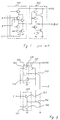
- the conventionally proposed BiCMOS logic circuit outputs inverted signals of logical product logical sum of the input signals in the NOR and NAND, and when a logical output of OR or AND is needed, an inverted logical signal is outputted from a CMOS logic circuit 401 as shown in Fig. 1, and inputted into an inverter circuit of BiCOMS 402 to obtain a normal signal as an output from the BiCMOS circuit.
- the inputs A, B and C are outputted from the CMOS logic circuit 401 as A ⁇ B+C ⁇ , and by inverting the same once again at the BiCMOS logic inverter 402, an output of A ⁇ B+C can be obtained.
- an error in estimating the load wiring length may result in insufficient driving capacity of the logic circuit and a buffer circuit capable of high capacitance driving at a high speed may have to be inserted between an output of the logic circuit and the load wiring. Since there are no circuits where inputs and outputs thereof are in the same phase in the BiCMOS circuit, the CMOS inverter and the BiCMOS inverter have to be serially connected and used as a buffer circuit.
- the semiconductor circuit according to the present invention comprises a CMOS logic circuit, a partial circuit where a first N-channel MOSFET is serially connected between the power source and the ground and the connection point thereof is used as an output, the first N-channel MOSFET having an NMOS logic unit of the same construction as the N-channel MOS of the CMOS logic circuit and a gate thereof which are connected to an output of the CMOS logic circuit, P-channel MOSFETs in each of which source is connected to a power source, the drains to an output of the partial circuit and the gate to an output of the CMOS logic circuit, an NPN bipolar transistors whose collector is connected to a power source and the base to an output point of the partial circuit, and second N-channel MOSFETs each of whose drains is connected to an emitter of said NPN bipolar transistor while acting as the output terminal, the gate connected to the output point of the CMOS logic circuit, and the source is grounded.
- Fig. 2 shows the diagram of a common-mode buffer circuit which is the first embodiment according to the present invention.
- a P-channel MOSFET (hereinafter "PMOS”) 107 and an N-channel MOSFET (hereinafter “NMOS”) 108 constitute a CMOS logic circuit 101 which outputs an inverted signal of an input I.
- the output of the CMOS circuit 101 is connected to the gate of an NMOS 106 whose drain is connected to the output terminal O and the source is grounded, to the gate of an NMOS 110 whose drain is connected to an NMOS logic unit 103 and the source is grounded, and to the gate of a PMOS 104 whose drain is connected to the output of a partial circuit 102 and the source is connected to the gate of a PMOS 104 whose source is connected to the power source.
- the partial circuit 102 comprising an NMOS 109 which constitutes the NMOS logic 103 and the NMOS 110 is a circuit which outputs a signal of the same phase as an input I, and its output point is connected to the base of an NPN bipolar transistor 105 whose collector is connected to the power source VDD, and the emitter to the output terminal O.
- the input I is switched from 1 to 0, the PMOS 107 is enabled and the NMOS 108 disenabled, whereby potential at the output of the CMOS logic 108 rises from the grounding potential to that of the VDD to turn on the NMOS 106.
- the NMOS 109 becomes disenabled as the level of the input I is shifted to 0, and the potential of the partial circuit 102 at the output point lowers toward that of the grounding as the NMOS 110 is connected at the gate thereof to the output of the CMOS logic circuit.
- the PMOS 104 becomes disenabled as its gate is connected to the output of the CMOS logic 101 to lower the base potential of the NPN bipolar transistor 105, which in turn becomes disenabled and its potential at the output O lowers to that of the grounding to output a signal of 0 level.
- the PMOS 107 becomes disenabled while the NMOS 108 is enabled, so that the potential at the output of the CMOS logic circuit 101 lowers toward the grounding potential to disenable the NMOS 106.
- the NMOS 109 becomes enabled first, and the potential of the partial circuit 102 at the output point starts to rise toward the potential which is determined by the resistance ratio between the NMOS 109 and the NMOS 110 when they are turned on.
- the NMOS 110 rapidly becomes disenabled while the PMOS 104 rapidly becomes enabled, the potential of the partial circuit 102 at the output point, or the base potential of the NPN bipolar transistor 105 rapidly rises toward the VDD potential, enabling the NPN bipolar transistor 105, while the potential at the output terminal O rises toward a value which is equivalent to the VDD potential minus the built-in-potential VF between the base and emitter of the NPN bipolar transistor 105 to become 1.
- a BiCMOS buffer circuit whose input and output are of the same phase is realized, such that when the input I is at 0 level, the output terminal O is also at 0 level, and when the input I is at 1 level the output terminal is at 1 level.
- the number of gates from the input terminal to the output terminal in the embodiment is also less as compared with the conventional circuit, realizing a high speed operation.
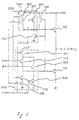
- the CMOS logic circuit 101a comprises PMOSs 201, 202, 203, and NMOSs 204, 205, 206.
- the NMOS logic unit 103a comprises NMOSs 208 and 209 in serial connection and an NMOS 207 which is in parallel connection therewith, the construction being the same as that of the CMOS logic circuit 101a on the NMOS side.
- Other features of the construction are the same as the first embodiment shown in Fig. 2.
- the output point of the partial circuit starts charging first through at least either one of the serial circuit comprising the NMOS 207 and NMOS 209 and the NMOS 207, and then rapidly becomes charged as the output of the CMOS logic circuit changes.
- a delay for three stages of logic gates in the conventional circuit shown in Fig. 1 when the same logic is to be realized a delay for only two logic gate stages occurs in the embodiment, enabling a high speed operation.
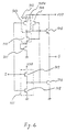
- Fig. 4 is a circuit diagram of the third embodiment according to the present invention, which differs from the first embodiment shown in Fig. 2 in construction in that the NMOS 109a is an NMOS with a small threshold voltage, and that an NMOS 301 which is small in threshold voltage similarly as the NMOS 109 and whose gate and drain are commonly connected is inserted between the partial circuit 102 and the ground.
- the threshold voltage of the NMOS 109a which constitutes the NMOS logic 103 is set at a low value, a high value is obtained in the initial charging at the output point of the partial circuit 102 when the input I is switched from 0 to 1, contributing to increased operational speed.
- the NMOS 301 is inserted, if the source potential of the NMOS 109a is increased by the amount of the threshold voltage of the NMOS 301 from the potential of the input I (grounding potential), the NMOS 109a can be maintained disenabled.
- the threshold voltages of the NMOSs 109a and 301 is preferably in the range of from 0.1 to 0.4 V for the reasons stated above.
- the present invention is effective as a common-mode buffer circuit, AND logic circuits and OR logic circuits can be structured with fewer stages of logic gates, realizing a high speed operation.
Landscapes
- Engineering & Computer Science (AREA)
- Physics & Mathematics (AREA)
- Computer Hardware Design (AREA)
- Computing Systems (AREA)
- General Engineering & Computer Science (AREA)
- Mathematical Physics (AREA)
- Power Engineering (AREA)
- Logic Circuits (AREA)
Applications Claiming Priority (2)
| Application Number | Priority Date | Filing Date | Title |
|---|---|---|---|
| JP327915/90 | 1990-11-28 | ||
| JP2327915A JP2570492B2 (ja) | 1990-11-28 | 1990-11-28 | 半導体回路 |
Publications (2)
| Publication Number | Publication Date |
|---|---|
| EP0488328A2 true EP0488328A2 (de) | 1992-06-03 |
| EP0488328A3 EP0488328A3 (en) | 1992-07-29 |
Family
ID=18204420
Family Applications (1)
| Application Number | Title | Priority Date | Filing Date |
|---|---|---|---|
| EP19910120452 Withdrawn EP0488328A3 (en) | 1990-11-28 | 1991-11-28 | Bi-cmos type semiconductor logic circuit |
Country Status (4)
| Country | Link |
|---|---|
| US (1) | US5247214A (de) |
| EP (1) | EP0488328A3 (de) |
| JP (1) | JP2570492B2 (de) |
| KR (1) | KR950000352B1 (de) |
Cited By (2)
| Publication number | Priority date | Publication date | Assignee | Title |
|---|---|---|---|---|
| EP0552963A3 (en) * | 1992-01-22 | 1993-12-08 | Samsung Semiconductor Inc | Noninverting logic gate |
| US8750320B2 (en) | 1997-01-23 | 2014-06-10 | Broadcom Corporation | Fibre channel arbitrated loop bufferless switch circuitry to increase bandwidth without significant increase in cost |
Families Citing this family (1)
| Publication number | Priority date | Publication date | Assignee | Title |
|---|---|---|---|---|
| US7554839B2 (en) * | 2006-09-30 | 2009-06-30 | Alpha & Omega Semiconductor, Ltd. | Symmetric blocking transient voltage suppressor (TVS) using bipolar transistor base snatch |
Family Cites Families (6)
| Publication number | Priority date | Publication date | Assignee | Title |
|---|---|---|---|---|
| JPS5490941A (en) * | 1977-12-26 | 1979-07-19 | Hitachi Ltd | Driving circuit of tristate type |
| EP0058958B1 (de) * | 1981-02-25 | 1986-10-29 | Kabushiki Kaisha Toshiba | Komplementäre MOSFET-Logikschaltung |
| EP0209805B1 (de) * | 1985-07-22 | 1993-04-07 | Hitachi, Ltd. | Halbleitereinrichtung mit bipolarem Transistor und Isolierschicht-Feldeffekttransistor |
| DE3878345T2 (de) * | 1987-08-17 | 1993-05-27 | Nippon Electric Co | Bimosschaltung, faehig zum betrieb bei hoher geschwindigkeit mit niedrigem verbrauch. |
| JP2569113B2 (ja) * | 1988-03-07 | 1997-01-08 | 株式会社日立製作所 | 半導体集積回路装置 |
| JPH02128515A (ja) * | 1988-11-08 | 1990-05-16 | Nec Corp | インバータ回路 |
-
1990
- 1990-11-28 JP JP2327915A patent/JP2570492B2/ja not_active Expired - Lifetime
-
1991
- 1991-11-28 KR KR1019910021488A patent/KR950000352B1/ko not_active Expired - Fee Related
- 1991-11-28 EP EP19910120452 patent/EP0488328A3/en not_active Withdrawn
- 1991-11-29 US US07/799,956 patent/US5247214A/en not_active Expired - Fee Related
Cited By (2)
| Publication number | Priority date | Publication date | Assignee | Title |
|---|---|---|---|---|
| EP0552963A3 (en) * | 1992-01-22 | 1993-12-08 | Samsung Semiconductor Inc | Noninverting logic gate |
| US8750320B2 (en) | 1997-01-23 | 2014-06-10 | Broadcom Corporation | Fibre channel arbitrated loop bufferless switch circuitry to increase bandwidth without significant increase in cost |
Also Published As
| Publication number | Publication date |
|---|---|
| JPH04196920A (ja) | 1992-07-16 |
| JP2570492B2 (ja) | 1997-01-08 |
| KR950000352B1 (ko) | 1995-01-13 |
| KR920011077A (ko) | 1992-06-27 |
| US5247214A (en) | 1993-09-21 |
| EP0488328A3 (en) | 1992-07-29 |
Similar Documents
| Publication | Publication Date | Title |
|---|---|---|
| EP0058958B1 (de) | Komplementäre MOSFET-Logikschaltung | |
| US4616146A (en) | BI-CMOS driver circuit | |
| US4779013A (en) | Slew-rate limited output driver having reduced switching noise | |
| EP0454135B1 (de) | MOS-Eingangsschaltung | |
| US5258666A (en) | CMOS clocked logic decoder | |
| US6198334B1 (en) | CMOS circuit | |
| US4961011A (en) | BiMOS current mirror | |
| EP0542227B1 (de) | Ausgangspufferschaltung | |
| US5047669A (en) | Tristate circuit using bipolar transistor and CMOS transistor | |
| US4871928A (en) | BICMOS driver circuit with complementary outputs | |
| US4682054A (en) | BICMOS driver with output voltage swing enhancement | |
| US4649295A (en) | BIMOS logic gate | |
| JP3240042B2 (ja) | 半導体出力回路 | |
| US5680069A (en) | Driver/receiver circuit including receiver circuit with p-channel MOSFET and N-channel MOSFET | |
| US5371419A (en) | CMOS well switching circuit | |
| US5663659A (en) | Semiconductor integrated circuit device comprising CMOS transistors and differentiator | |
| US5036226A (en) | Signal converting circuit | |
| EP0196113A2 (de) | Tri-state-Pufferschaltung | |
| EP0361841B1 (de) | Logische Bicmos-Schaltung | |
| US4880998A (en) | Bipolar transistor and CMOS transistor logic circuit having improved discharge capabilities | |
| EP0473409B1 (de) | BiCMOS logische Schaltung | |
| US5057713A (en) | Bipolar MOS logic circuit and semiconductor integrated circuit | |
| US4682052A (en) | Input buffer circuit | |
| US5138195A (en) | Bi-CMOS logic circuit having full voltage swing and rapid turn-off | |
| EP0488328A2 (de) | Bi-CMOS halbleiterlogische Schaltung |
Legal Events
| Date | Code | Title | Description |
|---|---|---|---|
| PUAI | Public reference made under article 153(3) epc to a published international application that has entered the european phase |
Free format text: ORIGINAL CODE: 0009012 |
|
| 17P | Request for examination filed |
Effective date: 19911128 |
|
| AK | Designated contracting states |
Kind code of ref document: A2 Designated state(s): DE FR GB |
|
| PUAL | Search report despatched |
Free format text: ORIGINAL CODE: 0009013 |
|
| AK | Designated contracting states |
Kind code of ref document: A3 Designated state(s): DE FR GB |
|
| 17Q | First examination report despatched |
Effective date: 19951016 |
|
| STAA | Information on the status of an ep patent application or granted ep patent |
Free format text: STATUS: THE APPLICATION HAS BEEN WITHDRAWN |
|
| 18W | Application withdrawn |
Withdrawal date: 19960216 |