EP0488031A2 - Method of and apparatus for inspecting a printed circuit board - Google Patents
Method of and apparatus for inspecting a printed circuit board Download PDFInfo
- Publication number
- EP0488031A2 EP0488031A2 EP91119738A EP91119738A EP0488031A2 EP 0488031 A2 EP0488031 A2 EP 0488031A2 EP 91119738 A EP91119738 A EP 91119738A EP 91119738 A EP91119738 A EP 91119738A EP 0488031 A2 EP0488031 A2 EP 0488031A2
- Authority
- EP
- European Patent Office
- Prior art keywords
- image
- hole
- pattern
- gauge
- operator
- Prior art date
- Legal status (The legal status is an assumption and is not a legal conclusion. Google has not performed a legal analysis and makes no representation as to the accuracy of the status listed.)
- Granted
Links
Images


Classifications
-
- G—PHYSICS
- G06—COMPUTING; CALCULATING OR COUNTING
- G06T—IMAGE DATA PROCESSING OR GENERATION, IN GENERAL
- G06T1/00—General purpose image data processing
-
- G—PHYSICS
- G06—COMPUTING; CALCULATING OR COUNTING
- G06T—IMAGE DATA PROCESSING OR GENERATION, IN GENERAL
- G06T7/00—Image analysis
- G06T7/0002—Inspection of images, e.g. flaw detection
- G06T7/0004—Industrial image inspection
- G06T7/0006—Industrial image inspection using a design-rule based approach
-
- G—PHYSICS
- G01—MEASURING; TESTING
- G01N—INVESTIGATING OR ANALYSING MATERIALS BY DETERMINING THEIR CHEMICAL OR PHYSICAL PROPERTIES
- G01N21/00—Investigating or analysing materials by the use of optical means, i.e. using sub-millimetre waves, infrared, visible or ultraviolet light
- G01N21/84—Systems specially adapted for particular applications
- G01N21/88—Investigating the presence of flaws or contamination
- G01N21/95—Investigating the presence of flaws or contamination characterised by the material or shape of the object to be examined
- G01N21/956—Inspecting patterns on the surface of objects
-
- G—PHYSICS
- G01—MEASURING; TESTING
- G01R—MEASURING ELECTRIC VARIABLES; MEASURING MAGNETIC VARIABLES
- G01R31/00—Arrangements for testing electric properties; Arrangements for locating electric faults; Arrangements for electrical testing characterised by what is being tested not provided for elsewhere
- G01R31/28—Testing of electronic circuits, e.g. by signal tracer
- G01R31/302—Contactless testing
- G01R31/308—Contactless testing using non-ionising electromagnetic radiation, e.g. optical radiation
- G01R31/309—Contactless testing using non-ionising electromagnetic radiation, e.g. optical radiation of printed or hybrid circuits or circuit substrates
-
- G—PHYSICS
- G06—COMPUTING; CALCULATING OR COUNTING
- G06T—IMAGE DATA PROCESSING OR GENERATION, IN GENERAL
- G06T7/00—Image analysis
- G06T7/60—Analysis of geometric attributes
- G06T7/62—Analysis of geometric attributes of area, perimeter, diameter or volume
-
- G—PHYSICS
- G01—MEASURING; TESTING
- G01N—INVESTIGATING OR ANALYSING MATERIALS BY DETERMINING THEIR CHEMICAL OR PHYSICAL PROPERTIES
- G01N21/00—Investigating or analysing materials by the use of optical means, i.e. using sub-millimetre waves, infrared, visible or ultraviolet light
- G01N21/84—Systems specially adapted for particular applications
- G01N21/88—Investigating the presence of flaws or contamination
- G01N21/95—Investigating the presence of flaws or contamination characterised by the material or shape of the object to be examined
- G01N21/956—Inspecting patterns on the surface of objects
- G01N2021/95638—Inspecting patterns on the surface of objects for PCB's
- G01N2021/95646—Soldering
-
- G—PHYSICS
- G01—MEASURING; TESTING
- G01N—INVESTIGATING OR ANALYSING MATERIALS BY DETERMINING THEIR CHEMICAL OR PHYSICAL PROPERTIES
- G01N21/00—Investigating or analysing materials by the use of optical means, i.e. using sub-millimetre waves, infrared, visible or ultraviolet light
- G01N21/84—Systems specially adapted for particular applications
- G01N21/88—Investigating the presence of flaws or contamination
- G01N21/95—Investigating the presence of flaws or contamination characterised by the material or shape of the object to be examined
- G01N21/956—Inspecting patterns on the surface of objects
- G01N2021/95638—Inspecting patterns on the surface of objects for PCB's
- G01N2021/95653—Through-holes
-
- G—PHYSICS
- G06—COMPUTING; CALCULATING OR COUNTING
- G06T—IMAGE DATA PROCESSING OR GENERATION, IN GENERAL
- G06T2207/00—Indexing scheme for image analysis or image enhancement
- G06T2207/30—Subject of image; Context of image processing
- G06T2207/30108—Industrial image inspection
- G06T2207/30141—Printed circuit board [PCB]
Landscapes
- Engineering & Computer Science (AREA)
- Physics & Mathematics (AREA)
- General Physics & Mathematics (AREA)
- Computer Vision & Pattern Recognition (AREA)
- Theoretical Computer Science (AREA)
- Health & Medical Sciences (AREA)
- Biochemistry (AREA)
- Pathology (AREA)
- Chemical & Material Sciences (AREA)
- Analytical Chemistry (AREA)
- Quality & Reliability (AREA)
- General Health & Medical Sciences (AREA)
- Immunology (AREA)
- Life Sciences & Earth Sciences (AREA)
- Geometry (AREA)
- Electromagnetism (AREA)
- Toxicology (AREA)
- General Engineering & Computer Science (AREA)
- Investigating Materials By The Use Of Optical Means Adapted For Particular Applications (AREA)
- Length Measuring Devices By Optical Means (AREA)
- Image Analysis (AREA)
- Image Processing (AREA)
Abstract
Description
- THE PRESENT INVENTION relates to a method of and an apparatus for inspecting the minimum annular width of a land formed on a printed circuit board, and more particularly to an improvement to reconcile accuracy and speed in the inspection.
- A printed circuit board is formed with wiring patterns having lands and through holes. Automatic inspection apparatus for the printed circuit board to automatically inspect the relative positions of the wiring patterns and through holes by reading the image of the printed circuit board have been developed and put to practical use. One of the significant points in the printed circuit board inspection is to check that a minimum annular width of a land remains after forming a through hole therein.
- Figure 28 illustrates an example of the conventional inspection of annular width of a land. A through
hole 2 is formed in aland 1. The throughhole 2 is deviated from the centre of theland 1 resulting from a drilling error or the like. In the inspection of annular width, binary images of a wiring pattern including theland 1 and the throughhole 2 are obtained. Aradial operator 3 is positioned such that its centre coincides with the centre of thethrough hole 2. A logical operation is performed between theradial operator 3 and the image of the wiring pattern. Theradial operator 3 has a plurality of arms. The annular widths of the land of the wiring pattern in the elongated directions of the respective arms are determined using a logic operation. Then, a minimum annular width WL is obtained which is the minimum value among the respective annular widths. When the minimum annular width WL is smaller than a threshold value, it is determined that the printed circuit board is defective. Such a radial operator is disclosed in Japanese Patent Application Laid-Open No. 62-263404, for example. - The direction in which the
through hole 2 deviates from the centre of theland 1 is not constant and varies in respective printed boards to be inspected. In order to determine accurately the minimum annular width, it is necessary to have a large number of arms of theradial operator 3. The high number of arms causes the time period required for the logic operation to grow longer so that the inspection is prevented from being performed at a high speed. Another problem is that the costs for manufacturing the inspection apparatus rise. - The present invention is directed to a method of, and an apparatus for, inspecting the minimum annular width of a land formed on a printed circuit board. The printed board is provided thereon with a wiring pattern having the land and a through hole surrounded by the land.
- According to one aspect the present invention provides a method which comprises the steps of: (a) obtaining a pattern image representing the shape of the wiring pattern and a hole image representing the shape of said through hole; (b) converting said hole image into a hole gauge image having an isotropic contour; (c) obtaining a pattern gauge image having a contour of the same shape as the pattern image; (d) obtaining a protrusion region image representative of part of the hole gauge image which protrudes from the pattern gauge image; and (e) comparing the size of the protrusion region image with a predetermined reference value to determine whether the minimum annular width of the land is larger than the reference value or not.
- The step (e) may comprise the steps of (e-1) scanning said protrusion region image with an operator having a size corresponding to said reference value; and (e-2) applying said operator to said protrusion region image in parallel with said scanning to thereby compare the size of said protrusion region image with said reference value.
- The operator may consist of a cluster of pixels, and the cluster of pixels may be a matrix array of pixels, in particular a cross-shaped array of pixels.
- In an aspect of the present invention, the pattern gauge image is obtained through the step of (c-1) defining the pattern gauge image by the pattern image itself.
- The hole gauge image may be generated through the steps of (b-1) enlarging the hole image by first and second enlargement widths different from each other to obtain first and second enlarged hole images, respectively; and (b-2) logically combining the first and second enlarged hole images to form a ring-like image around the hole image, the ring-like image being defined as the hole gauge image.
- In a preferred embodiment of the invention the step (e) comprises the steps of (e-3) designating said reference value and (e-4) determining a ring width of the ring-like image and the size of said operator as a function of said reference value.
- Preferably the step (e-4) comprises the steps of: (e-4-1) preparing a plurality of operators having different sizes; (e-4-2) selecting one of said plurality of operators according to said reference value to specify said operator; and (e-4-3) determining said ring width of said ring-like image as a function of the size of said operator selected and said reference value.
- In another aspect of the present invention, the hole gauge image is obtained through the step of (b-3) enlarging the hole image to define the hole gauge image.
- The pattern gauge image may be obtained through the steps of (c-2) logically combining the pattern image and the hole image to obtain a corrected image; and (c-3) obtaining the pattern gauge image from the corrected image.
- Preferably said pattern image has an annular image corresponding to said land, and a circular blank area which is surrounded by said annular image and has a size larger than said hole image; and the step (c-3) comprises the steps of (c-3-1) thickening respective parts of said corrected image to obtain an enlarged-and-corrected image in which said gap is eliminated; and (c-3-2) shrinking respective parts of said enlarged-and-corrected image to obtain said pattern gauge image.
- The present invention also provides an apparatus adapted to conduct the present method.
- Thus, in another aspect, the invention provides an apparatus for inspecting the minimum annular width of a land formed on a printed circuit board which is provided thereon with a wiring pattern having said land and a through hole perfectly or imperfectly surrounded by said land, said apparatus comprising:
- (a) means for obtaining a pattern image representing the shape of said wiring pattern and a hole image representing the shape of said through hole;
- (b) means for converting said hole image into a hole gauge image having an isotropic contour;
- (c) means for obtaining a pattern gauge image having a contour of the same shape as said pattern image;
- (d) means for obtaining a protrusion region image representative of part of said hole gauge image which protrudes from said pattern gauge image; and
- (e) means for comparing the size of said protrusion region image with a predetermined reference value to determine whether the minimum annular width of said land is larger than said reference value or not.
- Preferably the means (e) comprises (e-1) means for scanning said protrusion region image with an operator having a size corresponding to said reference value, and (e-2) means for applying said operator to said protrusion region image in parallel with said scanning to thereby compare the size of said protrusion region image with said reference value.
- The operator may consist of a cluster of pixels such as a matrix array of pixels and in particular the cluster of pixels is a cross-shaped array of pixels.
- In a preferred embodiment the obtaining means (c) comprises (c-1) means for defining said pattern gauge image by said pattern image itself.
- Advantageously the converting means (b) comprise (b-1) means for enlarging said hole image by first and second enlargement widths different from each other to obtain first and second enlarged hole images, respectively, and (b-2) means for logically combining said first and second enlarged hole images to form a ring-like image around said hole image, said ring-like image being defined as said hole gauge image.
- Preferably the comparing means comprise (e-3) means for inputting a signal designating said reference value, and (e-4) means for determining a ring width of the ring-like image and the size of said operator as a function of said reference value.
- Preferably the determining means (e-4) comprises (e-4-1) means for holding a plurality of operators having different sizes; (e-4-2) means for selecting one of said plurality of operators according to said reference value to specify said operator, and (e-4-3) means for determining said ring width of said ring-like image as a function of the size of said operator selected and said reference value.
- In another embodiment of the invention the converting means (b) comprise (b-3) means for enlarging said hole image to define the hole gauge image.
- In this embodiment the obtaining means (c) may comprise (c-2) means for logically combining said pattern image and said hole image to obtain a corrected image; and (c-3) means for obtaining said pattern gauge image from said corrected image.
- Preferably said pattern image has an annular image corresponding to said land, and a circular blank area which is surrounded by said annular image and has a size larger than said hole image, and the means (c-3) comprises (c-3-1) means for thickening respective parts of said corrected image to obtain an enlarged-and-corrected image in which said gap is eliminated; and (c-3-2) means for shrinking respective parts of said enlarged-and-corrected image to obtain said pattern gauge image.
- The deviation of the centre of the through hole from the centre of the land is in complementary relation to the minimum annular width, which is defined as the minimum value among annular widths at respective positions on the land. That is, the former is small when the latter is large, and vice versa. When the minimum annular width is large, the deviation of the centre of the through hole from the centre of the land is small, so that the hole gauge image having the isotropic contour does not protrude or protrudes slightly from the pattern gauge image having the contour of the same shape as the pattern image. Accordingly, the size of the protrusion region image is zero or small.
- When the minimum annular width is small, the size of the protrusion region image is large. In the present invention, the size of the protrusion region image is compared with the reference value to decide whether the minimum annular width is sufficient or not.
- The process step of comparing the size of the protrusion region image with the reference value may be attained by applying an operator having a size corresponding to the reference value to the protrusion region image.
- According to the present invention, since the minimum annular width is inspected by inspecting the size of the protrusion region image without applying a radial operator having arms to the land itself, the minimum annular width can be acculately inspected regardless of the direction in which the through hole is deviated from the land. Thus, a high-speed inspection can be achieved.
- An automatic inspection device for the printed circuit board, when applied to the present invention, does not need a complicated circuit which causes costs to rise.
- When an operator having a size corresponding to the reference value is applied to the protrusion region image, as in a preferred embodiment of the present invention, the minimum annular width is inspected simply and accurately.
- Employment of the ring-like image obtained from the first and second enlarged hole images prevents the false decision resulting from the influence of a gap which may appear between the pattern image and the hole image.
- The reference value may be variable. In this case, the sizes of the operator and ring-like image are accordingly changed. This prevents the false detection resulting from the broken pattern image when the minimum annular width is extremely small.
- On the other hand, when the hole gauge image is defined by enlarging the hole image, the substantial decrease of the minimum annular width due to employment of the first enlarged hole image can be eliminated to achieve a more accurate inspection.
- Further, when the pattern gauge image is defined by a corrected image obtained by combining the pattern image and the hole image, a false detection around the hole is prevented.
- The corrected image may be thickened and then shrinked to obtain the pattern gauge image, so that a gap which may appear in the corrected gauge image is eliminated to achieve a more accurate inspection.
- Preferred embodiments of the present invention provide a method of and an apparatus for inspecting the minimum annular width of a land on a printed circuit board accurately at a high speed.
- A preferred embodiment of the present invention provides an apparatus for inspecting a printed board which can be obtained at a low cost.
- The features, aspects and advantages of the present invention will become more apparent from the following detailed description of the present invention which is given by way of example with reference to the accompanying drawings, in which
- FIGURES 1 to 3 are block diagrams of structures for obtaining an image of a protrusion region and applying an operator to the image of the protrusion region according to first to third preferred embodiments of the present invention, respectively;
- FIGURE 4 shows an optical system for obtaining the image of a printed circuit board;
- FIGURE 5 illustrates relation between a land and a through hole, and
- FIGURE 6 is a block diagram of an electric circuitry employed in the apparatuses according to the respective preferred embodiments.
- Fig. 7 is a waveform chart showing the binarization of a pattern image and a through hole;
- Figs. 8 and 9 show relation in size between a blank portion of the pattern image and the through hole, respectively;
- Fig. 10 is a block diagram of a pre-processor;
- Fig. 11 is a block diagram of a variable enlargement circuit;
- Fig. 12 is a block diagram of a land inspection circuit;
- Fig. 13 is a block diagram of a two-dimensional shift register;
- Fig. 14 is a block diagram of an operator circuit;
- Figs. 15 to 18 illustrate the principle of detecting a minimum annular width;
- Fig. 19 illustrates the through hole in close proximity to an edge of the land;
- Fig. 20 illustrates an edge portion where the through hole is in close proximity to the edge of the land;
- Fig. 21 illustrates a pattern image with hole breakout;
- Figs. 22 to 25 illustrate changes in operator size and in ring width, respectively;
- Figs. 26 and 27 illustrate effects by double enlargement of a hole image, respectively; and
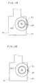
- Fig. 28 illustrates a conventional inspection of a minimum annular width using a radial operator.
- Fig. 4 schematically shows an image reading unit of an automatic inspection device for a printed circuit board according to a preferred embodiment of the present invention. A printed
circuit board 10 is formed with aconductive wiring pattern 12 on one or both surfaces of aninsulative base plate 11. As shown in the plan view of Fig. 5, thewiring pattern 12 includes aline part 13 and aland 14. There is provided a throughhole 15 pierceing theland 14 andinsulative base plate 11. - The through
hole 15 shown in Figs. 4 and 5 is a normal through hole for mounting electronic parts therethrough, which has a relatively large diameter. A through hole of another type is a mini via hole for connection between both surfaces of the printedcircuit board 10, which has a relatively small diameter. Both the normal through hole and the mini via hole are generically referred to as "through holes" in the present invention. - A
transmission light source 21 is disposed below the printedcircuit board 10, while reflectionlight sources 22 are disposed above the printedcircuit board 10. Light from thetransmission light source 21 passes through the throughhole 15 to reach anoptical head 20. Light from the reflectionlight sources 22 is reflected from the surface of the printedcircuit board 10 to reach theoptical head 20. The transmission and reflectionlight sources optical head 20 and are separated from each other by a dichroic mirror. Two CCD arrays also provided in theoptical head 20 detect the separated lights, respectively. Each of the CCD arrays transforms the light into an electric signal to produce a pattern image signal PS₀ representative of thewiring pattern 12 and a hole image signal HS₀ representative of the throughhole 15. Scanning for reading the images of respective parts of the printedcircuit board 10 can be achieved by moving the printedcircuit board 10 in the horizontal direction SX of Fig. 4. - The pattern image signal PS₀ and the hole image signal HS₀ are delivered to
binarizing circuits binarizing circuit 31 binarizes the pattern image signal PS₀ by comparing the pattern image signal PS₀ with a first threshold value TH1 shown in Fig. 7(a) to produce a digital pattern image signal PS. Thebinarizing circuit 32 compares the hole image signal HS₀ with a second threshold value TH2 to convert the hole image signal HS₀ into a digital hole image signal HS binarized. - It is ideal that the size of a blank portion PSH (Fig. 8) of the pattern image represented by the pattern image signal PS should be equal to that of a hole image HI represented by the hole image signal HS. However, the edge portions of the analog hole image signal HS₀ are inclined as shown in Fig. 7(b) resulting from light reflection from the inner wall of the through
hole 15 and the like. As a result, the size of the obtained hole image HS is not equal to and is smaller than that of the blank portion PSH as shown in Fig. 9. An improvement for compensating the deviation through data processing will be described later. - With reference again to Fig. 6, the binarized pattern image signal PS and hole image signal HS are delivered to a
pre-processor 100. The pre-processor 100 produces signals CHSt, CHSm, SHSt and SHSm, which will be described later, to output them to aland inspection circuit 200. The pattern image signal PS and the hole image signal HS are also inputted to theland inspection circuit 200. The details of theland inspection circuit 200 will be also described later. The inspection result of theland inspection circuit 200 is outputted as an inspection result signal INSc. - The pre-processor 100 supplements and reshapes the blank portion of the pattern image by performing a compensation processing on the pattern image signal PS to thereby produce a corrected pattern image signal CPS. The corrected pattern image signal CPS is supplied to a DRC (Design Rule Check)
circuit 310 and to acomparative inspection circuit 320. TheDRC circuit 310 extracts the characteristics of the pattern image and compares them with the CAD data of the printed circuit board. Thecomparative inspection circuit 320 compares the pattern image of the printed circuit board to be inspected with a non-defective pattern image previously stored in animage memory 330 to execute an appearance inspection of the printed circuit board. The inspection results of thecircuits - There is shown in detail in Fig. 10 part of the pre-processor 100 relevant to the processing of the hole image signal HS. The hole image signal HS is given to a
recognition circuit 112 in a recognition andclassification circuit 110. Therecognition circuit 112 detects the diameter of the throughhole 15 by applying a cross-shaped operator to the hole image and recognizes whether the throughhole 15 is a normal through hole or a mini via hole by comparing the diameter with a predetermined threshold value. The recognition result is indicated by a signal Sm. - The signal Sm and the hole image signal HS are outputted to a mini via
hole elimination circuit 113. The mini viahole elimination circuit 113 fills in the inside of the mini via hole to thereby produce a hole image signal HSt including only the normal through hole. - The hole image signal HS is also sent to a
delay circuit 111 and is delayed therein, so that timing is adjusted between the hole image signal HS and the signal HSt. The logical product of an inversion signal of the signal HSt and the signal HS is obtained in an ANDcircuit 114. A logical product signal HSm is a hole image signal including only the mini via hole. - The hole image signals HSt and HSm are inputted to an
enlargement circuit 120. The hole image signal HSm representative of the mini via hole is enlarged by the width of a predetermined number of pixels, e.g., by the width of one pixel, in anenlargement circuit 121 to be converted into the first enlarged hole image signal CHSm for the mini via hole. The first enlarged hole image signal CHSm is further enlarged in anenlargement circuit 123 to be converted into the second enlarged hole image signal SHSm. The first enlarged hole image signal CHSm which is subjected to a timing adjustment in adelay circuit 122 and the second enlarged hole image signal SHSm are outputted to the exterior of theenalrgement circuit 120. - Similarly, the hole image signal HSt representative of the normal through hole is enlarged by the width of a predetermined number of pixels, e.g., by the width of one pixel, in an
enlargement circuit 124 to be converted into the first enlarged hole image signal CHSt for the normal through hole. The first enlarged hole image signal CHSt is further enlarged in anenlargement circuit 126 to be converted into the second enlarged hole image signal SHSt. The first enlarged hole image signal CHSt which is subjected to a timing adjustment in adelay circuit 125 and the second enlarged hole image signal SHSt are outputted from theenlargement circuit 120. - Fig. 11 is a block diagram of the internal structure of the
enlargement circuit 126 for executing the second enlargement on the hole image of the normal through hole. Theenlargement circuit 123 for the mini via hole has the same structure. Theenlargement circuit 126 includes one-pixel enlargement circuits 131a to 131n for further enlarging the first enlarged hole image by the width of one pixel in sequential order. The number of one-pixel enlargement circuits 131a to 131n is, for example, twenty. All but the last one-pixel enlargement circuit 131n are fitted withdelay circuits 132a to 132(n-1) for timing adjustment. The one-pixel enlargement circuits 131a to 131n are connected in series, and the respective outputs thereof are given to aselector 133 in parallel. Thus theselector 133 receives n-number of enlarged hole image signals which are obtained by enlarging the first enlarged hole image signal CHSt by the width of i-number of pixels (i = 1 to n). Each of the one-pixel enlargement circuits 131a to 131n is adapted to perform a one-pixel enlargement processing in accordance with eight-point neighborhood enlargement logic, for example. - The printed circuit board inspection apparatus according to the preferred embodiment is equipped with a
control panel 50. Through manual operation of thecontrol panel 50, a reference value designation signal QR and an operator size designation signal QS described later are inputted to aselection signal generator 51. Theselection signal generator 51 produces a selection signal SEL1 based on the operator size designation signal QS to send it to theselector 133. Theselector 133 outputs one of the n-number of enlarged hole image signals in response to the selection signal SEL1 as the second enlarged hole image signal SHSt. - Hence, the
enlargement circuits - Fig. 12 is a block diagram of part of the
land inspection circuit 200 relevant to the preferred embodiment of the present invention. Theland inspection circuit 200 includes an annularwidth inspection circuit 200t for the normal through hole and an annularwidth inspection circuit 200m for the mini via hole. The annularwidth inspection circuits width inspection circuit 200t is described hereinafter, the structure and the operation of theother circuit 200m will be understood by those skilled in the art from the following description. - There is shown in Fig. 1 an example of the internal structure of the annular
width inspection circuit 200t. A pattern gauge signal PGS is obtained from the pattern image signal PS. Although the pattern gauge signal PGS is identical to the pattern signal PS in the preferred embodiment, the pattern gauge signal PGS may be a signal not identical but similar to the pattern signal PS. The pattern gauge signal PGS represents a pattern gauge image PGI, which is identical to the pattern image PI, in the preferred embodiment. The pattern gauge image signal PGS is inverted and input in an ANDcircuit 202. Another input of the andcircuit 202 is a hole gauge signal HGS representing a hole gauge image HGI. In this example, the hole gauge image HGI is a ring-like image RI, which is obtained by taking a logical product of an inversion signal of the first enlarged hole image signal CHSt and the second enlarged hole image signal SHSt. The output signal HGS (RIS) of the ANDcircuit 201 represents the ring-like image RI obtained by removing the first enlarged hole image EH1 from the second enlarged hole image EH2. The pattern gauge image PGI and the hole gauge image HGI reflect the shapes of the pattern image PI and the hole image HI, respectively. - When the inversion signal of the pattern gauge signal PGS and the hole gauge signal HGS are applied to the AND
circuit 202, the ANDcircuit 202 outputs a signal ES. The signal ES is a "protrusion region image signal" representative of part of the hole gauge image HGI which does not overlap the pattern gauge image PGI, that is, representative of a region ER protruding from the pattern gauge image PGI in the hole gauge image HGI. The protrusion region image signal ES is input to a two-dimensional shift register 210 for each pixel in series. - As shown in Fig. 13, the two-
dimensional shift register 210 includes four one-line delay circuits 211 to 214 and twenty-five unit registers R₁₁ to R₅₅ arranged in a 5x5 matrix form. Outputs S₁₁ to S₅₅ from the unit registers R₁₁ to R₅₅ correspond to the two-dimensional protrusion region image signal ES in a 5x5 pixel arrangement. The signals S₁₁ to S₅₅ are transmitted to an operator circuit 220 (Fig. 1) in parallel. - The
operator circuit 220 includes ANDcircuits 221 to 225 and aselector 226, as shown in Fig. 14. The ANDcircuit 221 receives the signals S₂₂, S₂₃, S₃₂ and S₃₃ constituting a 2x2 pixel matrix OP₄ and outputs the logical product PD₄ of the signals to theselector 226. Only when the pixel matrix OP₄ is positioned on a protrusion region image EI of Fig. 1, the logical product PD₄ is "1". For this reason, the pixel matrix OP₄ is an operator for a 2x2 pixel arrangement. - The other AND
circuits 222 to 225 operate similarily to the ANDcircuit 221. When an operator OP₉ for a rectangular cluster of nine pixels, an operator OP₁₂ for a cross-shaped cluster of twelve pixels, an operator OP₁₆ for a rectangular cluster of sixteen pixels, and an operator OP₂₅ for a rectangular cluster of twenty-five pixels are applied to the protrusion region image EI, their outputs are given to theselector 226 as logical product signals PD₉, PD₁₂, PD₁₆ and PD₂₅, respectively. The signal S₃₃ is also inputted to theselector 226 as a signal PD₁. The signal PD₁ corresponds to the operation result of an operator OP₁ having only one pixel. - The
selection signal generator 51 of Fig. 12 produces a selection signal SEL2 in response to the reference value designation signal QR and operator size designation signal QS and outputs the selection signal SEL2 to theselector 226 of Fig. 14. Theselector 226 selects one of the input signals PD₁ to PD₂₅ in response to the designation of the selection signal SEL2 to output the selected signal as the inspection result signal INSc. - This electrical operation corresponds to an operation for determining the minimum annular width of the through hole. The reason therefor will be described later in detail. Hereinafter, the operators OP₁ to OP₂₅ are represented by the reference character "OP", and the logical product signals PD₁ to PD₂₅ are represented by the reference character "PD".
- The operator OP corresponds to an approximately circular small region as shown in Fig. 15 since it is composed of a cluster of pixels. The logical product of "1" which is the result of applying the operator OP to the protrusion region image EI means that the size of the protrusion region image EI is larger than that of the operator OP. Since the center of the hole gauge image HGI coincides with the center of the through
hole 15, the protrusion region image EI of large size is equivalent to the large deviation of the throughhole 15 from the center of theland 14 so that the minimum annular width of theland 14 is small. - On the other hand, when the deviation of the through
hole 15 from the center of theland 14 is small as shown in Fig. 16, the size of the protrusion region image EI is small. In this case, the whole operator OP is not present within the protrusion region image EI, so that the result of applying the operator OP to the protrusion region image EI is constantly "0". Hence, if the signal PD of "1" is detected while the operator OP is scanning the protrusion region image EI, it is concluded that the minimum annular width is insufficient and the printed board is defective. Conversely, if the signal PD is always "0" during the scan, it is concluded that the minimum annular width is sufficient and the printed board is not defective. The scanning by the operator OP on the protrusion region image EI is automatically achieved by the scanning for reading the image of the printedcircuit board 10. - Preferably, the operator OP is a perfectly or approximately isotropic circle in shape. It is, however, difficult to provide a perfectly circular operator in the digital signal processing. In this preferred embodiment, the rectangular operators or the cross-shaped operators obtained by removing the pixels at the corners from the rectangular operators are employed as approximately circular operators.
- The reason for preparing the plurality of operators OP₁ to OP₂₅ and selectively using one of them will be described later.
- Next, the principle will be explained more quantitatively. Respective values shown in Fig. 17 are defined as follows:
- Lr:
- size of the operator OP (diameter of the circle);
- Lt:
- distance between the circumference of the through
hole 15 and the operator OP; - L:
- width of the hole gauge image HGI;
- La:
- minimum annular width of the land;
- Lb:
- distance between the circumference of the operator OP and the edge of the pattern gauge image PGI.
- The ring-like image RI described with reference to Fig. 1 may be used as the hole gauge image HGI. In this case, the width L is defined as the ring width of the ring-like image RI. Although the hole image HI and the blank portion PSH of the pattern image PI do not exactly coincide as discussed with reference to Fig. 9, it is assumed that they coincide approximately. The circumference of the blank portion PSH of the pattern image PI is taken as the circumference of the through
hole 15. In another case, an enlarged hole image EHI is used as the hole gauge image HGI, as described below. In this case, it is unnecessary to take into consideration the blank portion PSH corresponding to the throughhole 15 because the pattern gauge image PGI is a corrected pattern image CI in which the blank portion PSH is approximately compensated for (see Figs. 2 and 3) or a corrected pattern image DI in which the blank portion PSH is completely compensated for (see Fig. 2). Thus, the width L may be considered as the result of subtracting the radius of the through hole 15 (the radius of the hole image) from the radius of the enlarged hole image EHI. - As is apparent from Fig. 17, the following formulas hold:


- Accordingly,

- On the other hand, a condition for ensuring the necessary minimum annular width is:

where L₀ is a reference value of the minimum annular width. - Substitution of the formula (3) into the formula (4) gives:

- Since the boundary between sufficient and insufficient minimum annular widths should correspond to the state in which the operator OP is just fitted into the protrusion region image EI and the distance Lb of zero, the following formula is obtained as a criterion for discriminating the sufficient and insufficient minimum annular widths:

- That is, the width L of the hole gauge image HGI and the size Lr of the operator OP are determined so that the difference therebetween is equal to the reference value L₀ of the minimum annular width. This provides the result of "insufficient minimum annular width" because the formula (5) does not hold when the quantity Lb is plus as shown in Fig. 17. On the other hand, the result of "sufficient annular width" is obtained because the formula (5) holds when Lb is substantially minus as shown in Fig. 18.
- In this preferred embodiment, when the reference value L₀ is designated arbitrarily through the control panel 50 (Fig. 12), the signal QR representative of this value is input to the
selection signal generator 51. Theselection signal generator 51 calculates the width L of the hole gauge image HGI and the size Lr of the operator OP according to the formula (6). - As is recognized from the formula (6), there are a plurality of pairs of values (L, Lr) satisfying the formula (6). In this preferred embodiment, six values are prepared for the size Lr of the operator OP and one of them can be selected arbitrarily in response to the operator size designation signal QS. The preparation of the six operators OP₁ to OP₂₅ in the structure of Fig. 14 corresponds to the preparation of the six values for the size Lr. The operators OP₁ to OP₂₅ are different in size, and one of them is selected in response to the operator size designation signal QS. The reason for the variable size of the operator will be described later.
- When the size Lr of the operator is selected, the width L is uniquely determined from the formula (6). This determination can be achieved by storing a table corresponding to the formula (6) in the
selection signal generator 51. Preferably, different sets of values (L, Lr, L₀) are used for the normal through hole and the mini via hole. - The hole gauge image HGI and the pattern gauge image PGI are used for obtaining the protrusion region image EI. Since the peripheral portion of the hole gauge image HGI is relevant to the protrusion region image EI as mentioned above, the ring-like image RI shown in Fig. 1 can be used as the hole gauge image HGI. The principle for generating the ring-like image RI is as follows:
- As described with reference to Figs. 8 and 9, the size of the hole image HI is sometimes smaller than that of the blank portion PSH of the pattern image PS because of light reflection or light scattering at the inner wall of the through
hole 15. When the hole image HI itself is employed in place of the enlarged hole image EH1 for generating the ring-like image RI of Fig. 1, the size of a blank portion inside the ring-like image RI is smaller than that of the blank portion PSH of the pattern image PS, so that the output signal ES (Fig. 1) of the ANDcircuit 202 represents not only the protrusion region image EI but also an internal ring image NI, as shown in Fig. 26. As a result, when the operator OP is applied to the image represented by the signal ES, the internal ring image NI is also subjected to the operation. Then, a false result of "insufficient annular width" might be obtained even if the minimum annular width is a sufficient one. - On the other hand, when the ring-like image RI based on the difference between the first and second enlarged hole images EH1 and EH2 determined in advance as shown in Fig. 1 is employed, the blank portion PSH of the pattern image PI is prevented from overlapping the ring-like image RI as shown in Fig. 27. This operation is advantageous in that the inspection for determining the defective/non-defective in the minimum annular width can be accurately performed. However, when an optical system is used in which the size of the hole image HI approximately coincides with the size of the blank portion PSH of the pattern image PS, the ring-like image RI may be produced based on the difference between the enlarged ring-like image EH2 and the hole image HI itself. Further, when the size of the internal ring image NI can be estimated beforehand and the size of the operator OP is increased in proportion to the size of the internal ring image NI, the ring-like image RI may be produced based on the difference between the enlarged ring-like image EH2 and the hole image HI itself since the inspection result is not affected by the internal ring image NI.
- When the first enlarged hole image EH1 is employed to obtain the ring-like image RI, the annular width on the image plane. However, this decrease do not so affect the inspection of the annular width, and is avoided in the improvement according to another preferred embodiment described later.
- Figs. 2 and 3 show preferred embodiments in which the enlarged hole image EHI is used as the hole gauge image HGI. Unlike the preferred embodiment shown in Fig. 1, the corrected pattern image CI (Fig. 3) in which the blank portion PSH is approximately compensated for or the corrected pattern image DI (Fig. 2) in which the blank portion PSH is completely compensated for is used as the pattern gauge image PGI.
- The preferred embodiment of Fig. 2 is discussed first. To compensate for the blank portion PSH of the pattern image PI, the pattern image PI and the hole image HI are logically combined. That is, the signals PS and HS are input to an OR
circuit 203. The corrected image CI thereby provided has a gap for the above-mentioned reason as shown in Fig. 2. The compensation for the gap is carried out by thickening the corrected image CI in an enlargement-and-reduction processor 204 to eliminate the gap and then shrinking the thickened image to the original size. The signal corresponding to the resultant corrected image DI is the pattern gauge image signal PGS. The inversion signal of the pattern gauge image signal PGS is applied to one terminal of the ANDcircuit 202. - The enlarged hole image EHI used as the hole gauge image HGI is sent as the signal SHSt from the enlargement circuit 120 (Fig. 10) similarly to the second enlarged hole image EH2 shown in Fig. 1. The signal SHSt is applied to the other terminal of the AND
circuit 202 as the hole gauge image signal HGS. The ANDcircuit 202 outputs the protrusion region image signal ES. - Thus, when the corrected image DI including no blank portion PSH is used as the pattern gauge image PGI, the enlarged hole image EHI can be used as the hole gauge image HGI. The first enlarged hole image EH1 for defining the inner circumference of the ring-like image RI is not produced. Therefore, the above-mentioned substantial decrease of the minimum annular width is not caused, so that the minimum annular width can be inspected more accurately.
- The pattern gauge image PGI may be the corrected pattern image CI before compensation for the gap in the preferred embodiment of Fig. 3. The internal ring image NI is produced in this case similarly to the case where the ring-like image RI is produced by using the hole image HI in place of the first enlarged hole image EHI. However, the minimum annular width can be inspected by selecting the operator OP of suitable size if the size of the internal ring image NI is estimated beforehand.
- It is preferable that the size of the operator OP is variable for the above-mentioned reason. Another reason therefor is as follows:
- When the through
hole 15 is in close proximity to the edge of theland 14 as shown in Fig. 19, an edge portion PIE of the pattern image PI is ideally expected to be an elongated and continuous image as shown in Fig. 20. In practice, resulting from errors in optical reading of the pattern image PI or in signal processing, the pattern image PI is sometimes broken as shown in Fig. 21 so that only dotlike images DP are left. In this case, the printed circuit board may be regarded as non-defective as far as an electric connection is attained at the through hole. - When the pattern gauge image PGI is determined from this pattern image PI, part of the operator OP enters the gap between the dotlike images DP in some cases as shown in Figs. 22 and 24, so that the logical operation result by the operator OP becomes "1" (defective).
- As shown in Figs. 23 and 25, when the size of the operator OP is increased, the operator OP overlaps the dotlike images DP. The logical operation result by the operator OP constantly becomes "0" (non-defective) so that the aforesaid situation can be prevented. This structure is in general effective when the edge portion of the pattern gauge image PGI is broken without regard to the presence or absence of the dotlike images DP.
- To increase the size of the operator OP, the output selection in the
selector 226 of Fig. 14 is be changed. For example, when the broken edge of the pattern image PI which should be regarded as non-defective is decided to be defective by the operator OP₉, the selection signal SEL2 is changed through manual operation of thecontrol panel 50 to change the output of theselector 226 from the logical product signal PD₉ to PD₁₂. If the logical product signal PD₁₂ is still insufficient, the output of theselector 226 is changed to PD₁₆ or PD₂₅. Conversely, when the size of the operator OP is so large that the pattern which should be regarded as defective is decided to be non-defective, the selection should be changed to the operator of smaller size. The same is true for the processing of the internal ring image NI described in the previous section G. When it is known in advance that the width of the internal ring image NI is smaller than the size of the operator OP₉, the size of the operator OP is selected among the sizes of the operators OP₉ to OP₂₅. - When only the size of the operator OP is changed in this operation, the reference value to determine whether the minimum annular width is sufficient or not is substantially deviated from a designated value. In this preferred embodiment, change in the size Lr of the operator to be selected is accompanied by change in the width L of the hole gauge image HGI in accordance with the formula (6), so that the reference value L₀ is held at the same value as the value designated. That is, when the size of the operator is changed from Lr to Lr1, the width L is changed to L₁ obtained from the following formula:

- Thus the formula (8) corresponding to the formula (6) is always held.

- When the size Lr of the operator OP is increased, the width L is accordingly increased. When the size Lr of the operator OP is decreased, the width L is accordingly decreased. The calculation therefor is performed in the
selection signal generator 51. The width L is changed by changing the selection signal SEL1 applied to the selector 133 (Fig. 11). -
- (1) The optical system for reading the printed circuit board may be a system in which respective images of the wiring pattern and the through hole are obtained only from reflected light. In this case, the obtained analog signal is binarized with two different threshold values to determine the pattern image PI and the hole image HI.
- (2) It is preferable that the operator OP is of isotropic or approximately isotropic shape such as a circle or a polygon to inspect the size of the protrusion region image EI with uniform accuracy, since the protrusion region image EI may protrude from the pattern image PI in any direction. The operator OP, however, may be of other shape whose maximum width is of the designated size.
- (3) The present invention is also applicable to a case where the land is a circular or other-shaped land.
- While the invention has been shown and described in detail, the foregoing description is in all aspects illustrative and not restrictive. It is therefore understood that numerous modifications and variations can be devised without departing from the scope of the invention.
- The features disclosed in the foregoing description, in the claims and/or in the accompanying drawings may, both, separately and in any combination thereof, be material for realising the invention in diverse forms thereof.
Claims (14)
- A method of inspecting the minimum annular width of a land formed on a printed circuit board which is provided thereon with a wiring pattern having said land and a through hole perfectly or imperfectly surrounded by said land, said method comprising the steps of:(a) obtaining a pattern image representing the shape of said wiring pattern and a hole image representing the shape of said through hole;(b) converting said hole image into a hole gauge image having an isotropic contour;(c) obtaining a pattern gauge image having a contour of the same shape as said pattern image;(d) obtaining a protrusion region image representative of part of said hole gauge image which protrudes from said pattern gauge image; and(e) comparing the size of said protrusion region image with a predetermined reference value to determine whether the minimum annular width of said land is larger than said reference value or not.
- The method of Claim 1, wherein the step (e) comprises the steps of: (e-1) scanning said protrusion region image with an operator having a size corresponding to said reference value; and (e-2) applying said operator to said protrusion region image in parallel with said scanning to thereby compare the size of said protrusion region image with said reference value.
- The method of Claim 1 or 2 wherein the step (c) comprises the step of: (c-1) defining said pattern gauge image by said pattern image itself, and the step (b) comprises the steps of: (b-1) enlarging said hole image by first and second enlargement widths different from each other to obtain first and second enlarged hole images, respectively and (b-2) logically combining said first and second enlarged hole images to form a ring-like image around said hole image, said ring-like image being defined as said hole gauge image.
- The method of Claim 2, or Claim 3 as dependent thereon wherein the step (e) comprises the steps of: (e-3) designating said reference value; and (e-4) determining a ring width of the ring-like image and the size of said operator as a function of said reference value.
- The method of Claim 4 wherein the step (e-4) comprises the steps of: (e-4-1) preparing a plurality of operators having different sizes; (e-4-2) selecting one of said plurality of operators according to said reference value to specify said operator; and (e-4-3) determining said ring width of said ring-like image as a function of the size of said operator selected and said reference value.
- The method of Claim 1, wherein the step (b) comprises the step of (b-3) enlarging said hole image to define the hole gauge image; the step (c) comprises the steps of (c-2) logically combining said pattern image and said hole image to obtain a corrected image; and (c-3) obtaining said pattern gauge image from said corrected image, and said pattern image has an annular image corresponding to said land, and a circular blank area which is surrounded by said annular image and has a size larger than said hole image; and the step (c-3) comprises the steps of (c-3-1) thickening respective parts of said corrected image to obtain an enlarged-and-corrected image in which said gap is eliminated; and (c-3-2) shrinking respective parts of said enlarged-and-corrected image to obtain said pattern gauge image.
- An apparatus for inspecting the minimum annular width of a land formed on a printed circuit board which is provided thereon with a wiring pattern having said land and a through hole perfectly or imperfectly surrounded by said land, said apparatus comprising:(a) means for obtaining a pattern image representing the shape of said wiring pattern and a hole image representing the shape of said through hole;(b) means for converting said hole image into a hole gauge image having an isotropic contour;(c) means for obtaining a pattern gauge image having a contour of the same shape as said pattern image;(d) means for obtaining a protrusion region image representative of part of said hole gauge image which protrudes from said pattern gauge image; and(e) means for comparing the size of said protrusion region image with a predetermined reference value to determine whether the minimum annular width of said land is larger than said reference value or not.
- The apparatus of Claim 7 wherein the means (e) comprises (e-1) means for scanning said protrusion region image with an operator having a size corresponding to said reference value, and (e-2) means for applying said operator to said protrusion region image in parallel with said scanning to thereby compare the size of said protrusion region image with said reference value.
- The apparatus of Claim 5 or 7 wherein the means (c) comprises (c-1) means for defining said pattern gauge image by said pattern image itself.
- The apparatus of Claim 9 wherein the means (b) comprises (b-1) means for enlarging said hole image by first and second enlargement widths different from each other to obtain first and second enlarged hole images, respectively, and (b-2) means for logically combining said first and second enlarged hole images to form a ring-like image around said hole image, said ring-like image being defined as said hole gauge image.
- The apparatus of Claim 10 wherein the means (e) comprises (e-3) means for inputting a signal designating said reference value, and (e-4) means for determining a ring width of the ring-like image and the size of said operator as a function of said reference value.
- The apparatus of Claim 11 wherein the means (e-4) comprises (e-4-1) means for holding a plurality of operators having different sizes; (e-4-2) means for selecting one of said plurality of operators according to said reference value to specify said operator, and (e-4-3) means for determining said ring width of said ring-like image as a function of the size of said operator selected and said reference value.
- The apparatus of Claim 9 wherein the means (b) comprises (b-3) means for enlarging said hole image to define the hole gauge image.
- The apparatus of Claim 23 wherein the means (c) comprises (c-2) means for logically combining said pattern image and said hole image to obtain a corrected image; and (c-3) means for obtaining said pattern gauge image from said corrected image, and said pattern image has an annular image corresponding to said land, and a circular blank area which is surrounded by said annular image and has a size larger than said hole image, and the means (c-3) comprises (c-3-1) means for thickening respective parts of said corrected image to obtain an enlarged-and-corrected image in which said gap is eliminated; and (c-3-2) means for shrinking respective parts of said enlarged-and-corrected image to obtain said pattern gauge image.
Applications Claiming Priority (4)
| Application Number | Priority Date | Filing Date | Title |
|---|---|---|---|
| JP327161/90 | 1990-11-27 | ||
| JP32716190 | 1990-11-27 | ||
| JP198471/91 | 1991-07-12 | ||
| JP3198471A JP2500961B2 (en) | 1990-11-27 | 1991-07-12 | Printed circuit board residual inspection method |
Publications (3)
| Publication Number | Publication Date |
|---|---|
| EP0488031A2 true EP0488031A2 (en) | 1992-06-03 |
| EP0488031A3 EP0488031A3 (en) | 1992-10-07 |
| EP0488031B1 EP0488031B1 (en) | 1996-05-01 |
Family
ID=26510994
Family Applications (1)
| Application Number | Title | Priority Date | Filing Date |
|---|---|---|---|
| EP91119738A Expired - Lifetime EP0488031B1 (en) | 1990-11-27 | 1991-11-19 | Method of and apparatus for inspecting a printed circuit board |
Country Status (5)
| Country | Link |
|---|---|
| US (1) | US5408538A (en) |
| EP (1) | EP0488031B1 (en) |
| JP (1) | JP2500961B2 (en) |
| KR (1) | KR960002545B1 (en) |
| DE (1) | DE69119201D1 (en) |
Families Citing this family (16)
| Publication number | Priority date | Publication date | Assignee | Title |
|---|---|---|---|---|
| US5739846A (en) * | 1996-02-05 | 1998-04-14 | Universal Instruments Corporation | Method of inspecting component placement accuracy for each first selected circuit board to be assembled of a batch |
| JPH09222312A (en) * | 1996-02-16 | 1997-08-26 | Mitsui Mining & Smelting Co Ltd | Pattern inspection device and method |
| KR19980039100A (en) * | 1996-11-27 | 1998-08-17 | 배순훈 | Uninserted inspection device and method using the clinching direction of parts |
| US6275971B1 (en) * | 1997-09-30 | 2001-08-14 | Philips Electronics North America Corporation | Methods and apparatus for design rule checking |
| US6010939A (en) | 1998-03-31 | 2000-01-04 | Vlsi Technology, Inc. | Methods for making shallow trench capacitive structures |
| US6020616A (en) * | 1998-03-31 | 2000-02-01 | Vlsi Technology, Inc. | Automated design of on-chip capacitive structures for suppressing inductive noise |
| JP2002243656A (en) * | 2001-02-14 | 2002-08-28 | Nec Corp | Method and equipment for visual inspection |
| US8588511B2 (en) * | 2002-05-22 | 2013-11-19 | Cognex Corporation | Method and apparatus for automatic measurement of pad geometry and inspection thereof |
| JP2004127220A (en) * | 2002-10-01 | 2004-04-22 | Aisin Engineering Kk | Code reader |
| TWI275788B (en) * | 2004-09-09 | 2007-03-11 | Dainippon Screen Mfg | Method and apparatus for detecting a defect of an object by a color image of the object |
| CN101025398B (en) * | 2006-02-20 | 2010-06-02 | 牧德科技股份有限公司 | Hollow-bulge analyzing method for micro-pore after filled by copper |
| US8191018B1 (en) * | 2007-07-17 | 2012-05-29 | Kovio, Inc. | Methods and software for printing materials onto a substrate |
| SG158756A1 (en) * | 2008-07-10 | 2010-02-26 | Visionxtreme Pte Ltd | Hole inspection method and apparatus |
| JP6496159B2 (en) * | 2015-02-23 | 2019-04-03 | 株式会社Screenホールディングス | Pattern inspection apparatus and pattern inspection method |
| CN106290400A (en) * | 2016-07-29 | 2017-01-04 | 广东正业科技股份有限公司 | A kind of inspection hole method being applied to plate and inspection hole equipment |
| JP2021188937A (en) * | 2020-05-26 | 2021-12-13 | 株式会社デンソー | Extrusion inspection device and inspection method |
Citations (5)
| Publication number | Priority date | Publication date | Assignee | Title |
|---|---|---|---|---|
| FR2321229A1 (en) * | 1975-08-13 | 1977-03-11 | Cit Alcatel | METHOD AND APPARATUS FOR AUTOMATIC GRAPHIC CONTROL |
| US4040748A (en) * | 1975-06-30 | 1977-08-09 | International Business Machines Corporation | Inspection tool |
| GB2047879A (en) * | 1979-04-25 | 1980-12-03 | Hitachi Ltd | Photoelectric pcb inspection |
| US4980570A (en) * | 1990-02-23 | 1990-12-25 | Riken Denshi Co., Ltd | Device for determining location of apertures |
| DE3925911A1 (en) * | 1989-08-04 | 1991-02-07 | Siemens Ag | Opto-electronic test system for PCB - has circuit detecting bores in conductor path pattern ascertained by image converter |
Family Cites Families (6)
| Publication number | Priority date | Publication date | Assignee | Title |
|---|---|---|---|---|
| SE412966B (en) * | 1978-01-20 | 1980-03-24 | Danielsson Per Erik | DEVICE BETWEEN OBJECTS IN A TWO-DIMENSIONAL DISCRETEATED IMAGE |
| EP0054596B1 (en) * | 1980-12-18 | 1985-05-29 | International Business Machines Corporation | Process for inspecting and automatically classifying objects presenting configurations with dimensional tolerances and variable rejecting criteria depending on placement, apparatus and circuits therefor |
| US4555798A (en) * | 1983-06-20 | 1985-11-26 | Kla Instruments Corporation | Automatic system and method for inspecting hole quality |
| US5027417A (en) * | 1989-03-31 | 1991-06-25 | Dainippon Screen Mfg. Co., Ltd. | Method of and apparatus for inspecting conductive pattern on printed board |
| JP2524000B2 (en) * | 1991-02-22 | 1996-08-14 | 松下電器産業株式会社 | Pattern inspection device |
| US5119434A (en) * | 1990-12-31 | 1992-06-02 | Beltronics, Inc. | Method of and apparatus for geometric pattern inspection employing intelligent imaged-pattern shrinking, expanding and processing to identify predetermined features and tolerances |
-
1991
- 1991-07-12 JP JP3198471A patent/JP2500961B2/en not_active Expired - Fee Related
- 1991-11-19 DE DE69119201T patent/DE69119201D1/en not_active Expired - Lifetime
- 1991-11-19 EP EP91119738A patent/EP0488031B1/en not_active Expired - Lifetime
- 1991-11-22 KR KR1019910020986A patent/KR960002545B1/en not_active IP Right Cessation
-
1994
- 1994-08-01 US US08/283,982 patent/US5408538A/en not_active Expired - Fee Related
Patent Citations (5)
| Publication number | Priority date | Publication date | Assignee | Title |
|---|---|---|---|---|
| US4040748A (en) * | 1975-06-30 | 1977-08-09 | International Business Machines Corporation | Inspection tool |
| FR2321229A1 (en) * | 1975-08-13 | 1977-03-11 | Cit Alcatel | METHOD AND APPARATUS FOR AUTOMATIC GRAPHIC CONTROL |
| GB2047879A (en) * | 1979-04-25 | 1980-12-03 | Hitachi Ltd | Photoelectric pcb inspection |
| DE3925911A1 (en) * | 1989-08-04 | 1991-02-07 | Siemens Ag | Opto-electronic test system for PCB - has circuit detecting bores in conductor path pattern ascertained by image converter |
| US4980570A (en) * | 1990-02-23 | 1990-12-25 | Riken Denshi Co., Ltd | Device for determining location of apertures |
Also Published As
| Publication number | Publication date |
|---|---|
| JPH0520432A (en) | 1993-01-29 |
| KR960002545B1 (en) | 1996-02-22 |
| EP0488031B1 (en) | 1996-05-01 |
| JP2500961B2 (en) | 1996-05-29 |
| DE69119201D1 (en) | 1996-06-05 |
| US5408538A (en) | 1995-04-18 |
| KR920010255A (en) | 1992-06-26 |
| EP0488031A3 (en) | 1992-10-07 |
Similar Documents
| Publication | Publication Date | Title |
|---|---|---|
| EP0488031B1 (en) | Method of and apparatus for inspecting a printed circuit board | |
| EP0467149B1 (en) | Method of and device for inspecting pattern of printed circuit board | |
| US4578810A (en) | System for printed circuit board defect detection | |
| US5214712A (en) | Pattern inspection system for inspecting defect of land pattern for through-hole on printed board | |
| EP0466013B1 (en) | Method of and device for inspecting pattern of printed circuit board | |
| JPH06103165B2 (en) | How to measure the height of circuit elements on a board | |
| US5774573A (en) | Automatic visual inspection system | |
| JP2007071586A (en) | Image defect inspection device, image defect inspection system, defect classification device, and image defect inspection method | |
| US20060098863A1 (en) | Image defect inspection method, image defect inspection apparatus, and appearance inspection apparatus | |
| EP0488206A2 (en) | Method of and apparatus for inspecting pattern on printed board | |
| US5272761A (en) | Method and apparatus for inspecting line width on printed board | |
| JP2696000B2 (en) | Printed circuit board pattern inspection method | |
| JPH10135287A (en) | Wafer inspecting equipment and inspecting method | |
| JP2502853B2 (en) | Wiring pattern inspection device | |
| GB2139754A (en) | A pattern examining method | |
| JPH04286943A (en) | Method and apparatus for inspecting pattern of printed wiring board | |
| JP2007047122A (en) | Image defect inspection device, defect classification device, and image defect inspection method | |
| JPH0429041A (en) | Wiring pattern inspection device | |
| JP2524000B2 (en) | Pattern inspection device | |
| JP2002303588A (en) | Pattern defect inspection device | |
| JP2942171B2 (en) | Printed circuit board pattern inspection equipment | |
| JPH04319649A (en) | Through hole inspecting device | |
| JPH0658729A (en) | Inspecting apparatus for soldered state | |
| JPS591978B2 (en) | Object condition inspection device | |
| USRE38559E1 (en) | Automatic visual inspection system |
Legal Events
| Date | Code | Title | Description |
|---|---|---|---|
| PUAI | Public reference made under article 153(3) epc to a published international application that has entered the european phase |
Free format text: ORIGINAL CODE: 0009012 |
|
| AK | Designated contracting states |
Kind code of ref document: A2 Designated state(s): DE FR GB |
|
| PUAL | Search report despatched |
Free format text: ORIGINAL CODE: 0009013 |
|
| AK | Designated contracting states |
Kind code of ref document: A3 Designated state(s): DE FR GB |
|
| 17P | Request for examination filed |
Effective date: 19921223 |
|
| 17Q | First examination report despatched |
Effective date: 19940803 |
|
| GRAH | Despatch of communication of intention to grant a patent |
Free format text: ORIGINAL CODE: EPIDOS IGRA |
|
| GRAA | (expected) grant |
Free format text: ORIGINAL CODE: 0009210 |
|
| AK | Designated contracting states |
Kind code of ref document: B1 Designated state(s): DE FR GB |
|
| PG25 | Lapsed in a contracting state [announced via postgrant information from national office to epo] |
Ref country code: FR Effective date: 19960501 |
|
| REF | Corresponds to: |
Ref document number: 69119201 Country of ref document: DE Date of ref document: 19960605 |
|
| PG25 | Lapsed in a contracting state [announced via postgrant information from national office to epo] |
Ref country code: DE Effective date: 19960802 |
|
| EN | Fr: translation not filed | ||
| PLBE | No opposition filed within time limit |
Free format text: ORIGINAL CODE: 0009261 |
|
| STAA | Information on the status of an ep patent application or granted ep patent |
Free format text: STATUS: NO OPPOSITION FILED WITHIN TIME LIMIT |
|
| 26N | No opposition filed | ||
| REG | Reference to a national code |
Ref country code: GB Ref legal event code: IF02 |
|
| PGFP | Annual fee paid to national office [announced via postgrant information from national office to epo] |
Ref country code: GB Payment date: 20021113 Year of fee payment: 12 |
|
| PG25 | Lapsed in a contracting state [announced via postgrant information from national office to epo] |
Ref country code: GB Free format text: LAPSE BECAUSE OF NON-PAYMENT OF DUE FEES Effective date: 20031119 |
|
| GBPC | Gb: european patent ceased through non-payment of renewal fee |
Effective date: 20031119 |