EP0487901A2 - Disk controller using a video ram - Google Patents
Disk controller using a video ram Download PDFInfo
- Publication number
- EP0487901A2 EP0487901A2 EP91118091A EP91118091A EP0487901A2 EP 0487901 A2 EP0487901 A2 EP 0487901A2 EP 91118091 A EP91118091 A EP 91118091A EP 91118091 A EP91118091 A EP 91118091A EP 0487901 A2 EP0487901 A2 EP 0487901A2
- Authority
- EP
- European Patent Office
- Prior art keywords
- data
- buffer
- disk
- buffer memory
- bus
- Prior art date
- Legal status (The legal status is an assumption and is not a legal conclusion. Google has not performed a legal analysis and makes no representation as to the accuracy of the status listed.)
- Withdrawn
Links
Images

Classifications
-
- G—PHYSICS
- G06—COMPUTING OR CALCULATING; COUNTING
- G06F—ELECTRIC DIGITAL DATA PROCESSING
- G06F3/00—Input arrangements for transferring data to be processed into a form capable of being handled by the computer; Output arrangements for transferring data from processing unit to output unit, e.g. interface arrangements
- G06F3/06—Digital input from, or digital output to, record carriers, e.g. RAID, emulated record carriers or networked record carriers
- G06F3/0601—Interfaces specially adapted for storage systems
- G06F3/0628—Interfaces specially adapted for storage systems making use of a particular technique
- G06F3/0655—Vertical data movement, i.e. input-output transfer; data movement between one or more hosts and one or more storage devices
- G06F3/0656—Data buffering arrangements
Definitions
- This invention relates to disk memory control apparatus, and more particularly, to a disk controller that enables more efficient data transfers between a host processor and a disk memory.
- a buffer memory that is either implemented as a single-port, serial, random access memory (SRAM) or a single-port, dynamic, random access memory (DRAM).
- SRAM serial, random access memory
- DRAM dynamic, random access memory
- the buffer memory is connected via a bus to both input and output interface modules.
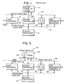
- FIG. 1 Such a disk controller is shown in FIG. 1 at the block diagram level.
- a buffer memory, 10 may be configured as either an SRAM or DRAM. The choice of a SRAM or DRAM buffer memory tends, to a large extent, to depend upon cost, required buffer bandwidth and desired application.
- a processor data bus 14 provides data access between buffer processor 12 and a host interface module 16, a buffer controller 18, a switch 20 and a disk mechanism interface 22.
- a buffer data bus 24 provides for data communication between host interface module 16 and buffer 10, and between buffer 10 and disk mechanism interface module 22.
- Switch 20 is also connected to buffer data bus 24 and provides for intercommunication between busses 14 and 24.
- Buffer controller 18, provides control and address signals via line 26 to buffer 10.
- buffer controller 18 The main function of buffer controller 18 is to arbitrate accesses to buffer 10 from external sources.
- Host interface module 16 provides a buffering function for data transfers between a host processor and buffer 10
- disk mechanism interface 22 provides a similar function between buffer 10 and a disk drive. All data transfers between buffer 10, host interface 16 and disk mechanism interface 22 occur over buffer data bus 24.
- buffer data bus 24 is a bottle-neck in the system and results in a substantial constriction on data transfers which can occur between the host processor and disk drive.
- Such DRAMS are called multi-port video RAM's (VRAM's) and include a DRAM portion (i.e., 262,144 words x 4 bits) and a serial access memory (SAM) portion (i.e., 512 words x 4 bits).
- DRAM digital versatile disk
- SAM serial access memory
- Such memories have dual ports that enable simultaneous access to both the DRAM and SAM. They furthermore have the ability to bi-directionally transfer data internally between the DRAM and a serial data register within the SAM. Memory accesses can occur simultaneously to and from the DRAM and to and from the SAM, except when data transfers are taking place internally between the DRAM and SAM.
- VRAM VRAM
- TMS 44C251, 262,144 4-bit, multi-port, video RAM from the Texas Instruments Corporation, Houston, Texas.
- a similarly functioning VRAM is available from Toshiba MOS Memory Products of Tokyo, Japan, and is denoted as the TC524256P/Z/J-10.
- Fig. 2 illustrates a block diagram of the Texas Instruments VRAM.
- Input/Output buffer section 27 provides independent access to and from DRAM 28.
- Input/Output buffer section 29 provides independent access to and from SAM 30.
- Data transfers between DRAM 28 and SAM 30 occur through data transfer gate 31. Address and control signals to accomplish data transfers are applied via inputs 32 and 33 respectively.
- VRAMS such as shown in Fig. 2, generally see use in graphics processors and associated control devices, but not with disk controllers.
- a disk controller is described with an improved buffer interface between a host processor and a disk drive.
- the disk controller includes a buffer memory having at least two ports, each port capable of bi-directional data transfers to and from the buffer memory.
- a first data bus is connected to one such port and a second data bus is connected to a second such port.
- a controller operates the buffer memory so that data transfers occur to and from the buffer memory simultaneously over the first and second data busses. This thereby enables more efficient data transfers to occur between the host processor and disk drive.
- FIG. 1 is a block diagram of a prior art disk controller.
- FIG. 2 is a block diagram of a prior art VRAM.
- FIG. 3 is a block diagram of a disk controller that includes the invention hereof.
- the buffer memory now comprises a video RAM (VRAM) buffer 34 that includes a DRAM 35 and SAM 36.
- VRAM 34 can be configured as shown in FIG. 2 or otherwise, so long as it has independent memory modules which are able to transfer data between themselves, and is additionally able to support independent external accesses to connected independent busses.
- a DRAM port 37 communicates with a DRAM data bus 38 while a SAM port 40 communicates with a SAM data bus 42.
- VRAM 34 supports bi-directional data transfers, simultaneously, in and out of ports 37 and 40. Data transfers are enabled between DRAM 35 and SAM 36, bi-directionally, under control of buffer controller 18. When such data transfers are occurring, in general, no data transfers take place from ports 37 or 40. The one exception is when a "split transfer" occurs internally between SAM 36 and DRAM 35. In such case, only one portion of a SAM row is caused to transfer. The other portion of the SAM row remains accessible from SAM port 40. Dram port 37 is not accessible from the outside in such a split transfer.
- SAM port 40 All data transfers to and from the host interface module 16 pass through SAM port 40 and are serial in nature. Transfer of data between SAM 36 and DRAM 35 occur by rows, internal to the VRAM. All other buffer data transfers are through DRAM port 37.
- Buffer controller 18 arbitrates all access requests to DRAM port 37 and performs SAM/DRAM data transfers, when required by SAM data movement.
- Buffer processor 12 performs the overall system control within the disk controller and assures that host interface module 16, buffer controller 18 and disk mechanism interface 22 operate in an interdependent and non-conflicting manner.
- Buffer controller 18 places SAM port 40 into an input mode. It then transfers the row of data from host interface module 16 into SAM 36 that contains the starting address within DRAM 35. A serial pointer is set to a desired column address for the first data byte. Data is then clocked into SAM port 36 from host interface module 16 until the row in SAM 36 is full. Buffer controller 18 then transfers the row of data from SAM 36 into the correct row in DRAM 35 and sets a serial pointer to the first column for the next row. Data is then clocked into SAM 36 until the row is full, and the row is then transferred to DRAM 35.
- VRAM buffer 34 Data may then be moved from VRAM buffer 34 to disk mechanism interface 22 through DRAM port 37. This is done as a regular DRAM-type access and may be accomplished in a page mode. Of course, such a data transfer may also be commenced prior to all data being "in place" within DRAM 35. These transfers continue until the entire data transfer is completed.
- Buffer processor 12 also has random access to VRAM buffer 34 via switch 20 through DRAM port 37. Refresh cycles and SAM/DRAM transfer commands occur as actions through DRAM port 37 as well. Buffer controller 18 arbitrates between a disk direct memory access, processor 12 accesses, SAM/DRAM transfer commands, and refresh cycles for DRAM 35. It is important to realize that access to DRAM and SAM ports 37 and 40 may occur simultaneously and independently.
- a data read appears very much like a data write operation.
- the data to be transferred to the host processor is placed in VRAM buffer 34 through DRAM port 37.
- Buffer controller 18 places SAM port 40 into the output mode, transfers from DRAM 35 to SAM 36 a row containing the first byte of data to be sent to the host computer and sets a serial pointer to the column address for the first byte.
- Data is then clocked out of SAM 36 and sent to host interface module 16, until the row in SAM 36 is empty.
- the next row of data is then transferred from DRAM 35 to SAM 36 and the serial pointer is set to the first column.
- the data is then clocked out and sent to host interface module 16.
- the process repeats until the last byte is clocked out and sent to host interface module 16. As that point, an interface direct memory access transfer is complete. Once again, accesses may occur simultaneously and independently to VRAM buffer 34 through both the SAM and DRAM ports 40 and 37 respectively, except, generally, during SAM/DRAM transfers.
- VRAM dual-port VRAM allows increased total buffer data transfer bandwidth by separating the host data transfers onto a different bus from remaining data transfers. Because data transfers can occur on both buses simultaneously, the RAM allows the use of a slower access time memory and/or a narrower buffer bus width, for a given total data transfer bandwidth, than a single port SRAM or DRAM buffer implementation.
Landscapes
- Engineering & Computer Science (AREA)
- Theoretical Computer Science (AREA)
- Human Computer Interaction (AREA)
- Physics & Mathematics (AREA)
- General Engineering & Computer Science (AREA)
- General Physics & Mathematics (AREA)
- Dram (AREA)
Abstract
Description
- This invention relates to disk memory control apparatus, and more particularly, to a disk controller that enables more efficient data transfers between a host processor and a disk memory.
- Conventional disk memory controllers employ a buffer memory that is either implemented as a single-port, serial, random access memory (SRAM) or a single-port, dynamic, random access memory (DRAM). The buffer memory is connected via a bus to both input and output interface modules. Such a disk controller is shown in FIG. 1 at the block diagram level. A buffer memory, 10 may be configured as either an SRAM or DRAM. The choice of a SRAM or DRAM buffer memory tends, to a large extent, to depend upon cost, required buffer bandwidth and desired application.
- The operation of the disk controller is supervised by a
dedicated buffer processor 12. Aprocessor data bus 14 provides data access betweenbuffer processor 12 and ahost interface module 16, abuffer controller 18, aswitch 20 and adisk mechanism interface 22. Abuffer data bus 24 provides for data communication betweenhost interface module 16 andbuffer 10, and betweenbuffer 10 and diskmechanism interface module 22. Switch 20 is also connected tobuffer data bus 24 and provides for intercommunication betweenbusses Buffer controller 18, on the other hand, provides control and address signals vialine 26 tobuffer 10. - The main function of
buffer controller 18 is to arbitrate accesses to buffer 10 from external sources.Host interface module 16 provides a buffering function for data transfers between a host processor andbuffer 10, whereasdisk mechanism interface 22 provides a similar function betweenbuffer 10 and a disk drive. All data transfers betweenbuffer 10,host interface 16 anddisk mechanism interface 22 occur overbuffer data bus 24. Thus, when a data transfer is occurring betweenbuffer 10 anddisk mechanism interface 22, no data transfers can occur betweenhost interface 16 and buffer 10 (and vice-versa). As a result,buffer data bus 24 is a bottle-neck in the system and results in a substantial constriction on data transfers which can occur between the host processor and disk drive. - Recently, a new type of DRAM has become available on the market for video applications. Such DRAMS are called multi-port video RAM's (VRAM's) and include a DRAM portion (i.e., 262,144 words x 4 bits) and a serial access memory (SAM) portion (i.e., 512 words x 4 bits). Such memories have dual ports that enable simultaneous access to both the DRAM and SAM. They furthermore have the ability to bi-directionally transfer data internally between the DRAM and a serial data register within the SAM. Memory accesses can occur simultaneously to and from the DRAM and to and from the SAM, except when data transfers are taking place internally between the DRAM and SAM. In certain cases, SAM data transfers can even continue when an internal data transfer is in process, but only from a portion of the SAM not involved in the internal transfer. One such VRAM is the TMS 44C251, 262,144 by 4-bit, multi-port, video RAM from the Texas Instruments Corporation, Houston, Texas. A similarly functioning VRAM is available from Toshiba MOS Memory Products of Tokyo, Japan, and is denoted as the TC524256P/Z/J-10.
- Fig. 2 illustrates a block diagram of the Texas Instruments VRAM. Input/
Output buffer section 27 provides independent access to and from DRAM 28. Input/Output buffer section 29 provides independent access to and fromSAM 30. Data transfers between DRAM 28 andSAM 30 occur throughdata transfer gate 31. Address and control signals to accomplish data transfers are applied viainputs - It is an object of this invention to provide an improved disk controller having higher data throughputs between a host processor and a disk drive.
- It is another object of this invention to provide a disk controller having improved buffer memory operation.
- It is a further object of this invention to employ a VRAM in a disk controller to enable improved data transfers.
- A disk controller is described with an improved buffer interface between a host processor and a disk drive. The disk controller includes a buffer memory having at least two ports, each port capable of bi-directional data transfers to and from the buffer memory. A first data bus is connected to one such port and a second data bus is connected to a second such port. A controller operates the buffer memory so that data transfers occur to and from the buffer memory simultaneously over the first and second data busses. This thereby enables more efficient data transfers to occur between the host processor and disk drive.
- FIG. 1 is a block diagram of a prior art disk controller.
- FIG. 2 is a block diagram of a prior art VRAM.
- FIG. 3 is a block diagram of a disk controller that includes the invention hereof.
- In FIG 3, like modules to those shown in FIG. 1 are numbered identically. It is to be noted that the buffer memory now comprises a video RAM (VRAM)
buffer 34 that includes aDRAM 35 andSAM 36. VRAM 34 can be configured as shown in FIG. 2 or otherwise, so long as it has independent memory modules which are able to transfer data between themselves, and is additionally able to support independent external accesses to connected independent busses. - A
DRAM port 37 communicates with aDRAM data bus 38 while aSAM port 40 communicates with a SAM data bus 42. As aforestated, VRAM 34 supports bi-directional data transfers, simultaneously, in and out ofports DRAM 35 andSAM 36, bi-directionally, under control ofbuffer controller 18. When such data transfers are occurring, in general, no data transfers take place fromports SAM 36 andDRAM 35. In such case, only one portion of a SAM row is caused to transfer. The other portion of the SAM row remains accessible from SAMport 40.Dram port 37 is not accessible from the outside in such a split transfer. - All data transfers to and from the
host interface module 16 pass throughSAM port 40 and are serial in nature. Transfer of data betweenSAM 36 andDRAM 35 occur by rows, internal to the VRAM. All other buffer data transfers are throughDRAM port 37. -
Buffer controller 18 arbitrates all access requests toDRAM port 37 and performs SAM/DRAM data transfers, when required by SAM data movement.Buffer processor 12 performs the overall system control within the disk controller and assures thathost interface module 16,buffer controller 18 anddisk mechanism interface 22 operate in an interdependent and non-conflicting manner. - A data write to the disk drive through
VRAM buffer 34 will now be described.Buffer controller 18places SAM port 40 into an input mode. It then transfers the row of data fromhost interface module 16 intoSAM 36 that contains the starting address withinDRAM 35. A serial pointer is set to a desired column address for the first data byte. Data is then clocked intoSAM port 36 fromhost interface module 16 until the row inSAM 36 is full.Buffer controller 18 then transfers the row of data fromSAM 36 into the correct row inDRAM 35 and sets a serial pointer to the first column for the next row. Data is then clocked intoSAM 36 until the row is full, and the row is then transferred toDRAM 35. - The above process is repeated until the data transfer from
host interface module 16 is complete, at which time the final row is transferred fromSAM 36 toDRAM 35 to complete a direct memory access transfer intoVRAM buffer 34. Data may then be moved fromVRAM buffer 34 todisk mechanism interface 22 throughDRAM port 37. This is done as a regular DRAM-type access and may be accomplished in a page mode. Of course, such a data transfer may also be commenced prior to all data being "in place" withinDRAM 35. These transfers continue until the entire data transfer is completed. -
Buffer processor 12 also has random access toVRAM buffer 34 viaswitch 20 throughDRAM port 37. Refresh cycles and SAM/DRAM transfer commands occur as actions throughDRAM port 37 as well.Buffer controller 18 arbitrates between a disk direct memory access,processor 12 accesses, SAM/DRAM transfer commands, and refresh cycles forDRAM 35. It is important to realize that access to DRAM andSAM ports - A data read appears very much like a data write operation. The data to be transferred to the host processor is placed in
VRAM buffer 34 throughDRAM port 37.Buffer controller 18places SAM port 40 into the output mode, transfers fromDRAM 35 to SAM 36 a row containing the first byte of data to be sent to the host computer and sets a serial pointer to the column address for the first byte. Data is then clocked out ofSAM 36 and sent to hostinterface module 16, until the row inSAM 36 is empty. The next row of data is then transferred fromDRAM 35 toSAM 36 and the serial pointer is set to the first column. The data is then clocked out and sent to hostinterface module 16. The process repeats until the last byte is clocked out and sent to hostinterface module 16. As that point, an interface direct memory access transfer is complete. Once again, accesses may occur simultaneously and independently toVRAM buffer 34 through both the SAM andDRAM ports - The use of a dual-port VRAM allows increased total buffer data transfer bandwidth by separating the host data transfers onto a different bus from remaining data transfers. Because data transfers can occur on both buses simultaneously, the RAM allows the use of a slower access time memory and/or a narrower buffer bus width, for a given total data transfer bandwidth, than a single port SRAM or DRAM buffer implementation.
- It should be understood that the foregoing description is only illustrative of the invention. Various alternatives and modifications can be devised by those skilled in the art without departing from the invention. Accordingly, the present invention is intended to embrace all such alternatives, modifications and variances which fall within the scope of the appended claims.
Claims (8)
- A disk controller for providing data transfers between a disk memory and a host processor, said disk controller exhibiting improved buffer memory data transfers, the combination comprising:
buffer memory means (34) having at least two ports (37, 40), each said port capable of bi-directional data transfers to and from said buffer memory means;
first bus means (42) connected to one said port (40) of said buffer memory means (34);
second bus means (38) connected to a second said port (37) of said buffer memory means (34), said first and second bus means (42, 38) capable of independent and simultaneous operation; and
control means (12, 18) for operating said buffer memory means so that data transfers occur to and from said buffer memory means (34) simultaneously over said first and second bus means. - The disk controller as claimed in Claim 1 wherein said buffer memory means comprises:
a video random access memory (VRAM) (34) including DRAM (35) and SAM (36) portions, said VRAM (34) including means for transfer of data between said DRAM and SAM portions. - The disk controller as recited in Claim 2 wherein one said port (40) provides bi-directional access to said SAM and a second said port (37) provides bi-directional access to said DRAM (34).
- The disk controller as claimed in Claims 2 or 3 wherein said control means comprises:
a microprocessor (12); and
a buffer controller (18), said buffer controller (18), under the control of said microprocessor (12), arbitrating data access reguests to said buffer memory and enabling internal data transfers between said SAM (36) and DRAM (35) within said VRAM (34). - The disk controller as recited in Claim 4, wherein said buffer controller (18) provides control and address signals via direct interconnections with said VRAM (34).
- The disk controller as claimed in any one of Claims 2 through 5 wherein said first bus means (42) is a data bus for enabling data flow between said VRAM (34) and a host interface module (16).
- The disk controller as claimed in any one of Claims 2 through 6 wherein said second bus means (38) is a data bus for enabling data flow between said VRAM (34) and a disk mechanism interface module (22).
- The disk controller as recited in any one of the preceding claims, comprising:
host interface means (16) connected between said first bus means (42) and a host processor and disk interface means (22) connected between said disk memory and said second bus (38), both said interface means functioning to control access between said buffer memory means (34) and said host processor and disk memory respectively.
Applications Claiming Priority (2)
| Application Number | Priority Date | Filing Date | Title |
|---|---|---|---|
| US62111590A | 1990-11-29 | 1990-11-29 | |
| US621115 | 2003-07-16 |
Publications (2)
| Publication Number | Publication Date |
|---|---|
| EP0487901A2 true EP0487901A2 (en) | 1992-06-03 |
| EP0487901A3 EP0487901A3 (en) | 1992-09-23 |
Family
ID=24488792
Family Applications (1)
| Application Number | Title | Priority Date | Filing Date |
|---|---|---|---|
| EP19910118091 Withdrawn EP0487901A3 (en) | 1990-11-29 | 1991-10-23 | Disk controller using a video ram |
Country Status (2)
| Country | Link |
|---|---|
| EP (1) | EP0487901A3 (en) |
| JP (1) | JPH04287217A (en) |
Cited By (4)
| Publication number | Priority date | Publication date | Assignee | Title |
|---|---|---|---|---|
| EP0756235A1 (en) * | 1995-07-24 | 1997-01-29 | Symbios Logic Inc. | Method and apparatus for enhancing throughput of disk array data transfers in a controller |
| EP0756234A1 (en) * | 1995-07-24 | 1997-01-29 | Symbios Logic Inc. | Method and apparatus for transferring data in a controller having a centralized memory |
| EP0578139A3 (en) * | 1992-07-06 | 1998-02-18 | Hewlett-Packard Company | Programmable disk drive array controller |
| US5875458A (en) * | 1994-06-16 | 1999-02-23 | International Business Machines Corporation | Disk storage device |
Family Cites Families (1)
| Publication number | Priority date | Publication date | Assignee | Title |
|---|---|---|---|---|
| JP2807010B2 (en) * | 1988-01-27 | 1998-09-30 | ストレイジ テクノロジー コーポレイション | Tape drive control unit for interconnection between host computer and tape drive and method of operating the same |
-
1991
- 1991-10-23 EP EP19910118091 patent/EP0487901A3/en not_active Withdrawn
- 1991-11-29 JP JP3340078A patent/JPH04287217A/en active Pending
Cited By (6)
| Publication number | Priority date | Publication date | Assignee | Title |
|---|---|---|---|---|
| EP0578139A3 (en) * | 1992-07-06 | 1998-02-18 | Hewlett-Packard Company | Programmable disk drive array controller |
| US5875458A (en) * | 1994-06-16 | 1999-02-23 | International Business Machines Corporation | Disk storage device |
| EP0756235A1 (en) * | 1995-07-24 | 1997-01-29 | Symbios Logic Inc. | Method and apparatus for enhancing throughput of disk array data transfers in a controller |
| EP0756234A1 (en) * | 1995-07-24 | 1997-01-29 | Symbios Logic Inc. | Method and apparatus for transferring data in a controller having a centralized memory |
| US5729705A (en) * | 1995-07-24 | 1998-03-17 | Symbios Logic Inc. | Method and apparatus for enhancing throughput of disk array data transfers in a controller |
| US5734848A (en) * | 1995-07-24 | 1998-03-31 | Symbios Logic Inc. | Method and appartus for transferring data in a controller having centralized memory |
Also Published As
| Publication number | Publication date |
|---|---|
| EP0487901A3 (en) | 1992-09-23 |
| JPH04287217A (en) | 1992-10-12 |
Similar Documents
| Publication | Publication Date | Title |
|---|---|---|
| US7386649B2 (en) | Multiple processor system and method including multiple memory hub modules | |
| KR100494201B1 (en) | Memory Systems, I / O Subsystem Devices, and How to Operate Memory Devices | |
| JP3976342B2 (en) | Method and apparatus for enabling simultaneous access to shared memory from multiple agents | |
| US6510098B1 (en) | Method and apparatus for transferring data in a dual port memory | |
| EP0919029B1 (en) | Memory control unit providing optimal timing of memory control sequences between different memory segments | |
| US5319388A (en) | VGA controlled having frame buffer memory arbitration and method therefor | |
| JP2002132701A (en) | Memory control unit | |
| US5416916A (en) | Structure for enabling direct memory-to-memory transfer with a fly-by DMA unit | |
| US6502173B1 (en) | System for accessing memory and method therefore | |
| US5167029A (en) | Data processing system and associated process using memory cards having data modify functions utilizing a data mask and an internal register | |
| EP0487901A2 (en) | Disk controller using a video ram | |
| US5802597A (en) | SDRAM memory controller while in burst four mode supporting single data accesses | |
| CN1132876A (en) | Bus arbitration between I/O devices and processing devices | |
| JPH0546527A (en) | Dual port memory circuit | |
| US6425020B1 (en) | Systems and methods for passively transferring data across a selected single bus line independent of a control circuitry | |
| JPS6326753A (en) | Memory bus control method | |
| JP2005346715A (en) | Multiport random access memory | |
| US6035372A (en) | Dynamic RAM in a microprocessor system | |
| EP0597296A2 (en) | Cache architecture for high speed memory-to-I/0 data transfers | |
| JPH01185758A (en) | Data bus matching device | |
| JPS63178320A (en) | Multiwindow display device | |
| JPH01266592A (en) | Image display system | |
| JPH07262125A (en) | Information processor | |
| JPH039453A (en) | Data transfer controller | |
| HK1007251A (en) | Dual port memories and systems and methods using the same |
Legal Events
| Date | Code | Title | Description |
|---|---|---|---|
| PUAI | Public reference made under article 153(3) epc to a published international application that has entered the european phase |
Free format text: ORIGINAL CODE: 0009012 |
|
| AK | Designated contracting states |
Kind code of ref document: A2 Designated state(s): DE FR GB IT |
|
| PUAL | Search report despatched |
Free format text: ORIGINAL CODE: 0009013 |
|
| AK | Designated contracting states |
Kind code of ref document: A3 Designated state(s): DE FR GB IT |
|
| 17P | Request for examination filed |
Effective date: 19930323 |
|
| STAA | Information on the status of an ep patent application or granted ep patent |
Free format text: STATUS: THE APPLICATION HAS BEEN WITHDRAWN |
|
| 18W | Application withdrawn |
Withdrawal date: 19931029 |
|
| R18W | Application withdrawn (corrected) |
Effective date: 19931029 |