EP0487325B1 - Procédé et dispositif pour inspecter les conducteurs d'un composant électronique - Google Patents
Procédé et dispositif pour inspecter les conducteurs d'un composant électronique Download PDFInfo
- Publication number
- EP0487325B1 EP0487325B1 EP91310699A EP91310699A EP0487325B1 EP 0487325 B1 EP0487325 B1 EP 0487325B1 EP 91310699 A EP91310699 A EP 91310699A EP 91310699 A EP91310699 A EP 91310699A EP 0487325 B1 EP0487325 B1 EP 0487325B1
- Authority
- EP
- European Patent Office
- Prior art keywords
- conductive leads
- integrated circuit
- circuit device
- heatable
- mounting
- Prior art date
- Legal status (The legal status is an assumption and is not a legal conclusion. Google has not performed a legal analysis and makes no representation as to the accuracy of the status listed.)
- Expired - Lifetime
Links
Images

Classifications
-
- H—ELECTRICITY
- H05—ELECTRIC TECHNIQUES NOT OTHERWISE PROVIDED FOR
- H05K—PRINTED CIRCUITS; CASINGS OR CONSTRUCTIONAL DETAILS OF ELECTRIC APPARATUS; MANUFACTURE OF ASSEMBLAGES OF ELECTRICAL COMPONENTS
- H05K13/00—Apparatus or processes specially adapted for manufacturing or adjusting assemblages of electric components
- H05K13/04—Mounting of components, e.g. of leadless components
- H05K13/046—Surface mounting
- H05K13/0465—Surface mounting by soldering
Definitions
- the present invention relates to the field of integrated circuit device assembly and inspection and particularly to systems and methods for the inspection of integrated circuit device conductive leads.
- the present invention provides apparatus for inspecting conductive leads of an integrated circuit device, the apparatus comprising: a hot bar thermode having one or more heatable blades for bonding conductive leads of an integrated circuit device to a mounting surface; means for mounting an integrated circuit device in a plane adjacent to the hot bar thermode whereby conductive leads of the integrated circuit device are disposed adjacent a surface of the one or more heatable blades; and means for illuminating the conductive leads disposed adjacent to a surface of one of the heatable blades at a low angle relative to the plane so as to highlight the conductive leads which shade the surface of the heatable blade thereby providing for visual inspection of the conductive leads.
- the present invention provides a method for inspecting conductive leads of an integrated circuit device, the method comprising the steps of: providing a hot bar thermode having one or more heatable blades for bonding conductive leads of an integrated circuit device to a mounting surface; mounting an integrated circuit device in a plane adjacent to the hot bar thermode whereby the conductive leads of the integrated circuit device are disposed adjacent to a surface of the one ore more heatable blades; and illuminating the conductive leads at a low angle with respect to the plane so as to highlight the conductive leads which shade the surface of the heatable blade, thereby creating a high contrast between the conductive leads and the plurality of heatable blades.
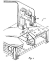
- inspection and assembly device 10 includes a mounting table 12 , which serves to support the various assembly and inspection areas which are illustrated thereon.
- circuit board assembly station 14 is illustrated and serves to accurately and rigidly mount a circuit board which will be populated by integrated circuit devices which are tested and assembled utilising the device as illustrated.
- a robotic arm 16 is preferably provided, in accordance with robotic techniques known in the prior art.
- Robotic arm 16 serves to mount a heating element or other device for bonding an integrated circuit device to a circuit.
- One such device is hot bar thermode tool 18 .
- Robotic arm 16 also serves to pick up, hold during inspection and place an integrated circuit device.
- device placement camera 20 is mounted to robotic arm 16 , which is utilised to accurately locate a placement site for each integrated circuit device.
- a vacuum pump and various control electronics 22 which are utilised, in accordance with methods known in the prior art, to control the movement of robotic arm 16 and to provide a vacuum to a vacuum chuck (not illustrated) within hot bar thermode tool 18 , so that an integrated circuit device may be selectively and temporarily held therein.
- inspection station 24 is utilised, in accordance with the method of the present invention, to provide an area wherein specific illumination is provided so that an integrated circuit device may be optically inspected.
- inspection aperture 26 Located within inspection station 24 is inspection aperture 26 , which serves to permit inspection camera 28 to focus on an integrated circuit device contained within hot bar thermode tool 18 when hot bar thermode tool 18 is positioned, by means of robotic arm 16 , directly above inspection aperture 26 .
- FIG. 2 there is depicted a plan view of the bottom of an integrated circuit which is held within the assembly device of Figure 1 .
- an integrated circuit 32 is depicted as held within hot bar thermode tool 18 .
- a vacuum chuck 44 is depicted and is utilised in conjunction with a vacuum pump to selectively and temporarily hold integrated circuit 32 within hot bar thermode tool 18 .
- hot bar thermode tool 18 includes a plurality of thermally activatable blades 34 , 36 , 38 , and 40 which are, in a preferred embodiment of the present invention electrically thermally activatable in order to assemble integrated circuit device 32 to a circuit board by melting solder in the vicinity of each conductive lead 42 .
- integrated circuit device 32 including a plurality of conductive leads 42 which overlay lower surfaces of the plurality of thermally activatable blades present within hot bar thermode tool 18 .
- thermally activatable blades 34 and 40 have been produced with a grained finish in a substantially single direction.
- This grained finish is preferably produced by grinding, sanding, lapping or any other grain producing operation. As long as the grain direction on the lower surface of thermally activatable blades 34 and 40 is produced in a single direction, the lower surfaces of thermally activatable blades 34 and 40 will act much like a Fresnel lens and will have a uniform and minimum specularity, appearing dark.
- Conductive leads 42 will have a uniform and highly reflective surface, appearing bright.
- the contrast between the lower surface of thermally activatable blade 34 and 42 and conductive leads 40 will be maximised by providing incident light 48 at an angle of between thirty and sixty degrees to the direction of the grain on the lower surfaces of thermally activatable blades 34 and 40 .
- incident light 48 is applied to the juncture of conductive leads 42 and the grained lower surfaces of thermally activatable blades 34 and 40 at an angle of approximately forty five degrees to the direction of the grain which is placed within the lower surface of thermallyl activatable blades 34 and 40 .
- inspection camera 28 (see Figure 1 ) may be utilised to provide an accurate visual inspection of conductive leads 42 while integrated circuit 32 is mounted within hot bar thermode tool 18 .
- This technique obviates the requirement of inspecting integrated circuit 32 in a first position and then subsequently transferring of integrated circuit 32 to an assembly position by picking the device up and moving it with a different tool.
- the elimination of this second transfer step renders the system much more efficient by eliminating the possibility that a conductive lead may be bent or damaged during a subsequent transfer of integrated circuit 32 .
- thermode tool shall mean any device which may be utilised to thermally mount an integrated circuit device to a circuit board.
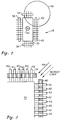
- inspection station 24 includes an inspection aperture 26 through which inspection camera 28 can provide an accurate optical inspection of conductive leads 42 of integrated circuit device 32 (see Figure 2 ).
- an integrated circuit device profile 50 is depicted within inspection aperture 26 and is generally rectangular or square in shape.
- integrated circuit devices of the type utilised in high density electronic systems typically have a plurality of conductive leads disposed along all four sides of a circuit device.
- a plurality of light stations 52 , 54 , 56 , 58 , 60 , 62 , 64 , and 66 are provided.
- Each of the aforementioned light station cooperates, as illustrated in Figure 4 , with a second light station which is disposed on a line opposite to its cooperating light station. That is, light station 54 cooperates with light station 60 to illuminate the left hand edge of integrated circuit device profile 50 . Similarly, light station 52 cooperates with light station 62 to illuminate the right hand edge of integrated circuit device profile 50 , and so on.
- each edge of an integrated circuit device can be thoroughly illuminated by utilising the plurality of light inspection stations depicted.
- each light station preferably comprises a dual stacked light with two sources of light focused utilising bi-convex lenses projecting oval patterns.
- Each light is preferably focused at an intermediate point along one of the thermally activatable blades of hot bar thermode tool 18 (see Figure 2 ) such that the conductive leads 42 disposed adjacent thereto will be illuminated.
- each light station By focusing the output of each light station at a low angle with respect to the plane wherein integrated circuit 32 (see Figure 2 ) is mounted the contrast between conductive leads 42 and each thermally activatable blade of hot bar thermode tool 18 may be enhanced by projecting a shadow on those portions of each thermally activatable blade which are exposed between adjacent conductive leads 42 . This technique will be illustrated in greater detail in Figure 5 herein.
- each light station mounted therein is connected via a fibre optic cable 70 to a light source 72 .
- the amount of illumination which is focused on each group of conductive leads 42 will preferably be substantially equal.
- the threshold levels which are utilised by inspection camera 28 to detect the presence or absence of a conductive lead may be accurately set for each edge of integrated circuit device 32 .
- FIG. 5 there is depicted a partial side view of an integrated circuit device which is mounted and illuminated in accordance with the embodiment of Figure 4 .
- a plurality of conductive leads 42 are disposed in an overlying relationship with thermally activatable blade 34 of hot bar thermode tool 18 .
- a low angle light source 54 such as provided by light station 54 , is then utilised to illuminated conductive leads 42 . Due to the fact that conductive leads 42 are tipically constructed of a gold or silver material and are highly reflective in nature, a great deal of light will be reflected from the surface of each conductive lead 42 , as illustrated at reference numerals 74 .
- a shadowed area 76 is provided on the lower surface of thermally activatable blade 34 of hot bar thermode tool 18 by the presence of each conductive lead 42 .
- each light station of inspection station 24 of Figure 4 is mounted so as to focus a beam of light on conductive leads 42 of integrated circuit device 32 at an angle of between ten and thirty degrees with respect to the plane in which integrated circuit device 32 is mounted.
- a method and apparatus in accordance with the present invention permits the visual inspection of electronic component leads during the mounting thereof.
- a hot bar thermode or other mounting tool or heating element having a plurality of thermally activatable blades has been described.
- a vacuum chuck and associated vacuum pump are utilised to selectively mount an integrated circuit device such that the conductive leads of the device are disposed adjacent to the lower surfaces of the thermally activatable blades.
- a low angle light source is then utilised to illuminate the integrated circuit device conductive leads such that a high contrast is created between the conductive leads and the lower surface of the thermally activatable blades, in order to permit an accurate visual inspection of the conductive leads.
- the lower surfaces of the thermally activatable blades are given a uniform grain by lapping those surfaces in a single direction to reduce the specularity of these surfaces and the angle of illumination is adjusted to enhance the contrast between the conductive leads and the lower blade surfaces.
- a camera disposed below the hot bar thermode may then be utilised to permit remote visual inspection of the conductive leads of an integrated circuit device while it is present within the mounting tool.
Landscapes
- Engineering & Computer Science (AREA)
- Manufacturing & Machinery (AREA)
- Microelectronics & Electronic Packaging (AREA)
- Testing Or Measuring Of Semiconductors Or The Like (AREA)
- Investigating Materials By The Use Of Optical Means Adapted For Particular Applications (AREA)
- Investigating Or Analyzing Materials Using Thermal Means (AREA)
Claims (8)
- Appareil pour inspecter les fils conducteurs d'un composant à circuit intégré, ledit appareil comprenant :une thermode à barre chaude (18) comprenant une ou plusieurs lames chauffables (34 à 40) pour souder les fils conducteurs (42) d'un composant à circuit intégré (32) à une surface de montage ;un élément (44) pour monter un composant à circuit intégré (32) dans un plan contigü à la thermode à barre chaude (18), les fils conducteurs (42) du composant à circuit intégré (32) étant disposés de manière contiguë à une surface d'au moins une des lames chauffables (34 à 40) ; caractérisé en ce qu'il comprend :un élément (54) pour éclairer les fils conducteurs (42) disposés de manière contiguë à une surface de l'une des lames chauffables (34) selon un angle plat par rapport au plan de façon à mettre en évidence les fils conducteurs (42) qui ombrent la surface (76) de la lame chauffante (34) pour permettre l'inspection visuelle des dits fils conducteurs (42).
- Appareil selon la revendication 1, dans lequel l'angle par rapport au plan est compris entre 10 et 30 degrés.
- Appareil selon la revendication 1 ou 2, dans lequel l'élément de montage comprend une ventouse (44) et un élément (22) pour activer sélectivement une pompe à vide associée.
- Appareil selon l'une quelconque des revendications précédentes comprenant, de plus, un appareil de prise de vue (28) pour fournir une image des fils conducteurs (42).
- Appareil selon l'une quelconque des revendications précédentes, dans lequel la surface de la lame chauffable (34) a un fini grainé, le grain ayant un sens donné.
- Appareil selon l'une quelconque des revendications précédentes, dans lequel le dispositif d'éclairage (54) est composé d'une source lumineuse (72) et d'une pluralité de câbles à fibre optique (70) pour diriger une pluralité de faisceaux lumineux (52 à 66) et éclairer, ainsi, les fils conducteurs (42) depuis des positions multiples.
- Appareil selon les revendications 1 à 5, dans lequel le dispositif d'éclairage (54) est composé d'au moins deux sources lumineuses focalisées sur les fils conducteurs (42) selon un angle compris entre trente et soixante degrés par rapport au dit sens du grain.
- Procédé pour inspecter les fils conducteurs d'un composant à circuit intégré, ledit procédé comprenant les étapes consistant à :prévoir une thermode à barre chaude (18) comprenant une ou plusieurs lames chauffables (34 à 40) pour souder les fils conducteurs (42) d'un composant à circuit intégré (32) à une surface de montage ;monter un composant à circuit intégré (32) dans un plan contigü à la thermode à barre chaude (18), les fils conducteurs (42) du composant à circuit intégré (32) étant disposés de manière contiguë à une surface d'au moins une des lames chauffables (34 à 40) ; ledit procédé étant caractérisé en ce qu'il comprend l'étape consistant à :éclairer les fils conducteurs (42) disposés de manière contiguë à une surface de l'une des lames chauffables (34) selon un angle plat par rapport au plan de façon à mettre en évidence les fils conducteurs (42) qui ombrent la surface (76) de la lame chauffante (34) pour permettre l'inspection visuelle des dits fils conducteurs (42).
Applications Claiming Priority (2)
| Application Number | Priority Date | Filing Date | Title |
|---|---|---|---|
| US61628790A | 1990-11-20 | 1990-11-20 | |
| US616287 | 1990-11-20 |
Publications (2)
| Publication Number | Publication Date |
|---|---|
| EP0487325A1 EP0487325A1 (fr) | 1992-05-27 |
| EP0487325B1 true EP0487325B1 (fr) | 1996-05-15 |
Family
ID=24468804
Family Applications (1)
| Application Number | Title | Priority Date | Filing Date |
|---|---|---|---|
| EP91310699A Expired - Lifetime EP0487325B1 (fr) | 1990-11-20 | 1991-11-20 | Procédé et dispositif pour inspecter les conducteurs d'un composant électronique |
Country Status (3)
| Country | Link |
|---|---|
| EP (1) | EP0487325B1 (fr) |
| JP (1) | JPH06103709B2 (fr) |
| DE (1) | DE69119555T2 (fr) |
Families Citing this family (2)
| Publication number | Priority date | Publication date | Assignee | Title |
|---|---|---|---|---|
| DE102005023705A1 (de) * | 2005-05-23 | 2006-11-30 | Siemens Ag | Sensor und Sensorsystem zur optischen Erfassung von Objekten, Bestückkopf, Verfahren zur Bestimmung der Höhenposition eines Bauelements |
| CN117020503B (zh) * | 2023-10-09 | 2023-12-22 | 云南流体规划研究院有限公司 | 一种浓硫酸液下节能泵叶轮焊接装置 |
Citations (1)
| Publication number | Priority date | Publication date | Assignee | Title |
|---|---|---|---|---|
| US3574923A (en) * | 1967-06-15 | 1971-04-13 | Western Electric Co | Compensating base for simultaneously bonding multiple leads |
Family Cites Families (2)
| Publication number | Priority date | Publication date | Assignee | Title |
|---|---|---|---|---|
| US4604648A (en) * | 1984-10-12 | 1986-08-05 | Kley Victor B | Electronic viewing system for integrated circuit packages |
| US4728195A (en) * | 1986-03-19 | 1988-03-01 | Cognex Corporation | Method for imaging printed circuit board component leads |
-
1991
- 1991-09-24 JP JP3270551A patent/JPH06103709B2/ja not_active Expired - Lifetime
- 1991-11-20 DE DE69119555T patent/DE69119555T2/de not_active Expired - Fee Related
- 1991-11-20 EP EP91310699A patent/EP0487325B1/fr not_active Expired - Lifetime
Patent Citations (1)
| Publication number | Priority date | Publication date | Assignee | Title |
|---|---|---|---|---|
| US3574923A (en) * | 1967-06-15 | 1971-04-13 | Western Electric Co | Compensating base for simultaneously bonding multiple leads |
Also Published As
| Publication number | Publication date |
|---|---|
| JPH06103709B2 (ja) | 1994-12-14 |
| DE69119555T2 (de) | 1996-11-21 |
| DE69119555D1 (de) | 1996-06-20 |
| JPH04313252A (ja) | 1992-11-05 |
| EP0487325A1 (fr) | 1992-05-27 |
Similar Documents
| Publication | Publication Date | Title |
|---|---|---|
| CN106920762B (zh) | 半导体制造装置、半导体器件的制造方法及芯片贴装机 | |
| US5195234A (en) | Method and apparatus for visual alignment of parts | |
| KR100870693B1 (ko) | 자동화된 광학 검사 시스템을 위한 조명 장치 | |
| US5257714A (en) | Method and apparatus for electronic component lead inspection | |
| US5962862A (en) | Method and apparatus for verifying the presence or absence of a component | |
| JPH05503797A (ja) | 半導体ウエハ上の識別マークを読み取るための装置および方法 | |
| US5307154A (en) | Semiconductor chip position detector | |
| KR19990081927A (ko) | 캐리어상에 콤포넌트를 배치하기 위한 방법과 배치기및, 이러한방법과 배치기에 사용되는 보정 캐리어 검출 장치 | |
| US5450206A (en) | Process and device for checking the conformity of hybridization balls | |
| KR20190032195A (ko) | 반도체 제조 장치 및 반도체 장치의 제조 방법 | |
| EP0487325B1 (fr) | Procédé et dispositif pour inspecter les conducteurs d'un composant électronique | |
| US6258495B1 (en) | Process for aligning work and mask | |
| JP2000099158A (ja) | ワークとマスクの整合機構および整合方法 | |
| US5570184A (en) | Method and apparatus for locating the position of lasing gaps for precise alignment and placement of optoelectric components | |
| JPH11267868A (ja) | レ―ザ加工装置及びレ―ザ加工方法 | |
| JPH0639762A (ja) | 部品供給装置 | |
| KR19980042720A (ko) | 전자부품관찰장치 및 전자부품관찰방법 | |
| GB2249672A (en) | Circuit board and apparatus for recognizing the position of a circuit board | |
| US7190393B2 (en) | Camera with improved illuminator | |
| CN111725086B (zh) | 半导体制造装置以及半导体器件的制造方法 | |
| US20030066952A1 (en) | Computer vision recognition of metallic objects against a poorly contrasting background | |
| US5923772A (en) | Method and apparatus for visual recognition of a component supplied to an industrial automated system | |
| US6291830B1 (en) | Methods and apparatus for controlling glint in a position alignment sensor | |
| JP2005505942A (ja) | 表面実装機検査カメラ上に用いる自動フィルタ交換器 | |
| US20240149363A1 (en) | Quality determination device and quality determination method |
Legal Events
| Date | Code | Title | Description |
|---|---|---|---|
| PUAI | Public reference made under article 153(3) epc to a published international application that has entered the european phase |
Free format text: ORIGINAL CODE: 0009012 |
|
| AK | Designated contracting states |
Kind code of ref document: A1 Designated state(s): DE FR GB |
|
| 17P | Request for examination filed |
Effective date: 19920917 |
|
| 17Q | First examination report despatched |
Effective date: 19941019 |
|
| GRAH | Despatch of communication of intention to grant a patent |
Free format text: ORIGINAL CODE: EPIDOS IGRA |
|
| GRAA | (expected) grant |
Free format text: ORIGINAL CODE: 0009210 |
|
| AK | Designated contracting states |
Kind code of ref document: B1 Designated state(s): DE FR GB |
|
| PG25 | Lapsed in a contracting state [announced via postgrant information from national office to epo] |
Ref country code: FR Effective date: 19960515 |
|
| REF | Corresponds to: |
Ref document number: 69119555 Country of ref document: DE Date of ref document: 19960620 |
|
| EN | Fr: translation not filed | ||
| PG25 | Lapsed in a contracting state [announced via postgrant information from national office to epo] |
Ref country code: GB Effective date: 19961120 |
|
| PLBE | No opposition filed within time limit |
Free format text: ORIGINAL CODE: 0009261 |
|
| STAA | Information on the status of an ep patent application or granted ep patent |
Free format text: STATUS: NO OPPOSITION FILED WITHIN TIME LIMIT |
|
| 26N | No opposition filed | ||
| GBPC | Gb: european patent ceased through non-payment of renewal fee |
Effective date: 19961120 |
|
| PG25 | Lapsed in a contracting state [announced via postgrant information from national office to epo] |
Ref country code: DE Effective date: 19970801 |