EP0487325B1 - Method and apparatus for electronic component lead inspection - Google Patents
Method and apparatus for electronic component lead inspection Download PDFInfo
- Publication number
- EP0487325B1 EP0487325B1 EP91310699A EP91310699A EP0487325B1 EP 0487325 B1 EP0487325 B1 EP 0487325B1 EP 91310699 A EP91310699 A EP 91310699A EP 91310699 A EP91310699 A EP 91310699A EP 0487325 B1 EP0487325 B1 EP 0487325B1
- Authority
- EP
- European Patent Office
- Prior art keywords
- conductive leads
- integrated circuit
- circuit device
- heatable
- mounting
- Prior art date
- Legal status (The legal status is an assumption and is not a legal conclusion. Google has not performed a legal analysis and makes no representation as to the accuracy of the status listed.)
- Expired - Lifetime
Links
Images

Classifications
-
- H—ELECTRICITY
- H05—ELECTRIC TECHNIQUES NOT OTHERWISE PROVIDED FOR
- H05K—PRINTED CIRCUITS; CASINGS OR CONSTRUCTIONAL DETAILS OF ELECTRIC APPARATUS; MANUFACTURE OF ASSEMBLAGES OF ELECTRICAL COMPONENTS
- H05K13/00—Apparatus or processes specially adapted for manufacturing or adjusting assemblages of electric components
- H05K13/04—Mounting of components, e.g. of leadless components
- H05K13/046—Surface mounting
- H05K13/0465—Surface mounting by soldering
Definitions
- the present invention relates to the field of integrated circuit device assembly and inspection and particularly to systems and methods for the inspection of integrated circuit device conductive leads.
- the present invention provides apparatus for inspecting conductive leads of an integrated circuit device, the apparatus comprising: a hot bar thermode having one or more heatable blades for bonding conductive leads of an integrated circuit device to a mounting surface; means for mounting an integrated circuit device in a plane adjacent to the hot bar thermode whereby conductive leads of the integrated circuit device are disposed adjacent a surface of the one or more heatable blades; and means for illuminating the conductive leads disposed adjacent to a surface of one of the heatable blades at a low angle relative to the plane so as to highlight the conductive leads which shade the surface of the heatable blade thereby providing for visual inspection of the conductive leads.
- the present invention provides a method for inspecting conductive leads of an integrated circuit device, the method comprising the steps of: providing a hot bar thermode having one or more heatable blades for bonding conductive leads of an integrated circuit device to a mounting surface; mounting an integrated circuit device in a plane adjacent to the hot bar thermode whereby the conductive leads of the integrated circuit device are disposed adjacent to a surface of the one ore more heatable blades; and illuminating the conductive leads at a low angle with respect to the plane so as to highlight the conductive leads which shade the surface of the heatable blade, thereby creating a high contrast between the conductive leads and the plurality of heatable blades.
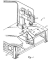
- inspection and assembly device 10 includes a mounting table 12 , which serves to support the various assembly and inspection areas which are illustrated thereon.
- circuit board assembly station 14 is illustrated and serves to accurately and rigidly mount a circuit board which will be populated by integrated circuit devices which are tested and assembled utilising the device as illustrated.
- a robotic arm 16 is preferably provided, in accordance with robotic techniques known in the prior art.
- Robotic arm 16 serves to mount a heating element or other device for bonding an integrated circuit device to a circuit.
- One such device is hot bar thermode tool 18 .
- Robotic arm 16 also serves to pick up, hold during inspection and place an integrated circuit device.
- device placement camera 20 is mounted to robotic arm 16 , which is utilised to accurately locate a placement site for each integrated circuit device.
- a vacuum pump and various control electronics 22 which are utilised, in accordance with methods known in the prior art, to control the movement of robotic arm 16 and to provide a vacuum to a vacuum chuck (not illustrated) within hot bar thermode tool 18 , so that an integrated circuit device may be selectively and temporarily held therein.
- inspection station 24 is utilised, in accordance with the method of the present invention, to provide an area wherein specific illumination is provided so that an integrated circuit device may be optically inspected.
- inspection aperture 26 Located within inspection station 24 is inspection aperture 26 , which serves to permit inspection camera 28 to focus on an integrated circuit device contained within hot bar thermode tool 18 when hot bar thermode tool 18 is positioned, by means of robotic arm 16 , directly above inspection aperture 26 .
- FIG. 2 there is depicted a plan view of the bottom of an integrated circuit which is held within the assembly device of Figure 1 .
- an integrated circuit 32 is depicted as held within hot bar thermode tool 18 .
- a vacuum chuck 44 is depicted and is utilised in conjunction with a vacuum pump to selectively and temporarily hold integrated circuit 32 within hot bar thermode tool 18 .
- hot bar thermode tool 18 includes a plurality of thermally activatable blades 34 , 36 , 38 , and 40 which are, in a preferred embodiment of the present invention electrically thermally activatable in order to assemble integrated circuit device 32 to a circuit board by melting solder in the vicinity of each conductive lead 42 .
- integrated circuit device 32 including a plurality of conductive leads 42 which overlay lower surfaces of the plurality of thermally activatable blades present within hot bar thermode tool 18 .
- thermally activatable blades 34 and 40 have been produced with a grained finish in a substantially single direction.
- This grained finish is preferably produced by grinding, sanding, lapping or any other grain producing operation. As long as the grain direction on the lower surface of thermally activatable blades 34 and 40 is produced in a single direction, the lower surfaces of thermally activatable blades 34 and 40 will act much like a Fresnel lens and will have a uniform and minimum specularity, appearing dark.
- Conductive leads 42 will have a uniform and highly reflective surface, appearing bright.
- the contrast between the lower surface of thermally activatable blade 34 and 42 and conductive leads 40 will be maximised by providing incident light 48 at an angle of between thirty and sixty degrees to the direction of the grain on the lower surfaces of thermally activatable blades 34 and 40 .
- incident light 48 is applied to the juncture of conductive leads 42 and the grained lower surfaces of thermally activatable blades 34 and 40 at an angle of approximately forty five degrees to the direction of the grain which is placed within the lower surface of thermallyl activatable blades 34 and 40 .
- inspection camera 28 (see Figure 1 ) may be utilised to provide an accurate visual inspection of conductive leads 42 while integrated circuit 32 is mounted within hot bar thermode tool 18 .
- This technique obviates the requirement of inspecting integrated circuit 32 in a first position and then subsequently transferring of integrated circuit 32 to an assembly position by picking the device up and moving it with a different tool.
- the elimination of this second transfer step renders the system much more efficient by eliminating the possibility that a conductive lead may be bent or damaged during a subsequent transfer of integrated circuit 32 .
- thermode tool shall mean any device which may be utilised to thermally mount an integrated circuit device to a circuit board.
- inspection station 24 includes an inspection aperture 26 through which inspection camera 28 can provide an accurate optical inspection of conductive leads 42 of integrated circuit device 32 (see Figure 2 ).
- an integrated circuit device profile 50 is depicted within inspection aperture 26 and is generally rectangular or square in shape.
- integrated circuit devices of the type utilised in high density electronic systems typically have a plurality of conductive leads disposed along all four sides of a circuit device.
- a plurality of light stations 52 , 54 , 56 , 58 , 60 , 62 , 64 , and 66 are provided.
- Each of the aforementioned light station cooperates, as illustrated in Figure 4 , with a second light station which is disposed on a line opposite to its cooperating light station. That is, light station 54 cooperates with light station 60 to illuminate the left hand edge of integrated circuit device profile 50 . Similarly, light station 52 cooperates with light station 62 to illuminate the right hand edge of integrated circuit device profile 50 , and so on.
- each edge of an integrated circuit device can be thoroughly illuminated by utilising the plurality of light inspection stations depicted.
- each light station preferably comprises a dual stacked light with two sources of light focused utilising bi-convex lenses projecting oval patterns.
- Each light is preferably focused at an intermediate point along one of the thermally activatable blades of hot bar thermode tool 18 (see Figure 2 ) such that the conductive leads 42 disposed adjacent thereto will be illuminated.
- each light station By focusing the output of each light station at a low angle with respect to the plane wherein integrated circuit 32 (see Figure 2 ) is mounted the contrast between conductive leads 42 and each thermally activatable blade of hot bar thermode tool 18 may be enhanced by projecting a shadow on those portions of each thermally activatable blade which are exposed between adjacent conductive leads 42 . This technique will be illustrated in greater detail in Figure 5 herein.
- each light station mounted therein is connected via a fibre optic cable 70 to a light source 72 .
- the amount of illumination which is focused on each group of conductive leads 42 will preferably be substantially equal.
- the threshold levels which are utilised by inspection camera 28 to detect the presence or absence of a conductive lead may be accurately set for each edge of integrated circuit device 32 .
- FIG. 5 there is depicted a partial side view of an integrated circuit device which is mounted and illuminated in accordance with the embodiment of Figure 4 .
- a plurality of conductive leads 42 are disposed in an overlying relationship with thermally activatable blade 34 of hot bar thermode tool 18 .
- a low angle light source 54 such as provided by light station 54 , is then utilised to illuminated conductive leads 42 . Due to the fact that conductive leads 42 are tipically constructed of a gold or silver material and are highly reflective in nature, a great deal of light will be reflected from the surface of each conductive lead 42 , as illustrated at reference numerals 74 .
- a shadowed area 76 is provided on the lower surface of thermally activatable blade 34 of hot bar thermode tool 18 by the presence of each conductive lead 42 .
- each light station of inspection station 24 of Figure 4 is mounted so as to focus a beam of light on conductive leads 42 of integrated circuit device 32 at an angle of between ten and thirty degrees with respect to the plane in which integrated circuit device 32 is mounted.
- a method and apparatus in accordance with the present invention permits the visual inspection of electronic component leads during the mounting thereof.
- a hot bar thermode or other mounting tool or heating element having a plurality of thermally activatable blades has been described.
- a vacuum chuck and associated vacuum pump are utilised to selectively mount an integrated circuit device such that the conductive leads of the device are disposed adjacent to the lower surfaces of the thermally activatable blades.
- a low angle light source is then utilised to illuminate the integrated circuit device conductive leads such that a high contrast is created between the conductive leads and the lower surface of the thermally activatable blades, in order to permit an accurate visual inspection of the conductive leads.
- the lower surfaces of the thermally activatable blades are given a uniform grain by lapping those surfaces in a single direction to reduce the specularity of these surfaces and the angle of illumination is adjusted to enhance the contrast between the conductive leads and the lower blade surfaces.
- a camera disposed below the hot bar thermode may then be utilised to permit remote visual inspection of the conductive leads of an integrated circuit device while it is present within the mounting tool.
Description
- The present invention relates to the field of integrated circuit device assembly and inspection and particularly to systems and methods for the inspection of integrated circuit device conductive leads.
- The increasing complexity of electronic systems along with a concomitant increase in packaging densities has resulted in an increased utilisation of automated device handling. Modern robotic systems are often utilised to assemble electronic systems and bring an increased reliability to highly repetitive operations, such as integrated circuit device mounting and placement. Often an integrated circuit device is picked up by a robotic arm and placed on a circuit board to be temporarily held in place by a tacky substance, such as flux. Subsequently, a hot bar thermode, or other similar device is utilised to permanently bond the device to the circuit board.
- Despite the increased efficiency and accuracy of robotic systems in placing and mounting integrated circuit devices on circuit boards, it is still necessary to inspect each integrated circuit device prior to mounting the device to ensure that the device is in a proper orientation and that all conductive leads are present and properly oriented to ensure proper conductive mounting. In the prior art this is often accomplished by utilising optical inspection techniques prior to placing each integrated circuit device at a mounting location; however, these systems require each integrated circuit device to be moved into an inspection area, inspected, and the moved again to the mounting position.
- Experience with such systems has shown that it is likely that an integrated circuit device may be damaged after inspection during the process of transporting that device to a mounting point. A need exists for a method and apparatus which permits an integrated circuit device to be inspected prior to mounting the device without requiring unnecessary handling of the device. One problem which must be overcome in such a system in the difficulty which is encountered in attempting to optically inspect an integrated circuit device while such device is present within a mounting tool, within the bonding tool shown in US-A-3 574 923.
- Viewed from one aspect the present invention provides apparatus for inspecting conductive leads of an integrated circuit device, the apparatus comprising: a hot bar thermode having one or more heatable blades for bonding conductive leads of an integrated circuit device to a mounting surface; means for mounting an integrated circuit device in a plane adjacent to the hot bar thermode whereby conductive leads of the integrated circuit device are disposed adjacent a surface of the one or more heatable blades; and means for illuminating the conductive leads disposed adjacent to a surface of one of the heatable blades at a low angle relative to the plane so as to highlight the conductive leads which shade the surface of the heatable blade thereby providing for visual inspection of the conductive leads.
- Viewed from another aspect the present invention provides a method for inspecting conductive leads of an integrated circuit device, the method comprising the steps of: providing a hot bar thermode having one or more heatable blades for bonding conductive leads of an integrated circuit device to a mounting surface; mounting an integrated circuit device in a plane adjacent to the hot bar thermode whereby the conductive leads of the integrated circuit device are disposed adjacent to a surface of the one ore more heatable blades; and illuminating the conductive leads at a low angle with respect to the plane so as to highlight the conductive leads which shade the surface of the heatable blade, thereby creating a high contrast between the conductive leads and the plurality of heatable blades.
- In order that the invention may be fully understood preferred embodiments thereof will now be described, by way of example only, with reference to the accompanying drawings in which:
- Figure 1 is a pictorial representation of an integrated circuit inspection and assembly device constructed in accordance with the present invention;
- Figure 2 is a plan view of the bottom of an integrated circuit mounted within the assembly device of Figure 1;
- Figure 3 is an exploded view of a portion of the integrated circuit and assembly device of Figure 2;
- Figure 4 is a pictorial representation of an inspection site and illumination system which may be utilised with an embodiment of the present invention; and
- Figure 5 is a partial side view of an integrated circuit device mounted and illuminated in accordance with the embodiment of Figure 4.
- With reference now to the figures and in particular with reference to Figure 1, there is depicted a pictorial representation of an integrated circuit inspection and assembly device constructed in accordance with the present invention. As is illustrated, inspection and
assembly device 10 includes a mounting table 12, which serves to support the various assembly and inspection areas which are illustrated thereon. For example, circuit board assembly station 14 is illustrated and serves to accurately and rigidly mount a circuit board which will be populated by integrated circuit devices which are tested and assembled utilising the device as illustrated. - A
robotic arm 16 is preferably provided, in accordance with robotic techniques known in the prior art.Robotic arm 16 serves to mount a heating element or other device for bonding an integrated circuit device to a circuit. One such device is hotbar thermode tool 18.Robotic arm 16 also serves to pick up, hold during inspection and place an integrated circuit device. Also mounted torobotic arm 16 isdevice placement camera 20, which is utilised to accurately locate a placement site for each integrated circuit device. - Situated beneath mounting table 12 are a vacuum pump and
various control electronics 22, which are utilised, in accordance with methods known in the prior art, to control the movement ofrobotic arm 16 and to provide a vacuum to a vacuum chuck (not illustrated) within hotbar thermode tool 18, so that an integrated circuit device may be selectively and temporarily held therein. - Also depicted on the upper surface of mounting table 12 is
inspection station 24.Inspection station 24 is utilised, in accordance with the method of the present invention, to provide an area wherein specific illumination is provided so that an integrated circuit device may be optically inspected. Located withininspection station 24 isinspection aperture 26, which serves to permitinspection camera 28 to focus on an integrated circuit device contained within hotbar thermode tool 18 when hotbar thermode tool 18 is positioned, by means ofrobotic arm 16, directly aboveinspection aperture 26. - Referring now to Figure 2, there is depicted a plan view of the bottom of an integrated circuit which is held within the assembly device of Figure 1. As is illustrated, an integrated
circuit 32 is depicted as held within hotbar thermode tool 18. Avacuum chuck 44 is depicted and is utilised in conjunction with a vacuum pump to selectively and temporarily hold integratedcircuit 32 within hotbar thermode tool 18. - As is illustrated, hot
bar thermode tool 18 includes a plurality of thermallyactivatable blades integrated circuit device 32 to a circuit board by melting solder in the vicinity of eachconductive lead 42. As is depicted in Figure 2,integrated circuit device 32, including a plurality ofconductive leads 42 which overlay lower surfaces of the plurality of thermally activatable blades present within hotbar thermode tool 18. - With reference now to Figures 2 and 3,
area 46 of integratedcircuit 32 and hotbar thermode tool 18 is shown in an exploded view within Figure 3. As is illustrated, a plurality ofconductive leads 42, which are electrically connected to selected portions of integratedcircuit 32, are positioned in an overlying fashion with respect to the lower surfaces of thermallyactivatable blades activatable blades - This grained finish is preferably produced by grinding, sanding, lapping or any other grain producing operation. As long as the grain direction on the lower surface of thermally
activatable blades activatable blades - Conductive leads 42, however, typically constructed of a gold or silver metallic substance, will have a uniform and highly reflective surface, appearing bright. The contrast between the lower surface of thermally
activatable blade conductive leads 40 will be maximised by providing incident light 48 at an angle of between thirty and sixty degrees to the direction of the grain on the lower surfaces of thermallyactivatable blades - In a preferred embodiment of the present invention, incident light 48 is applied to the juncture of
conductive leads 42 and the grained lower surfaces of thermallyactivatable blades activatable blades conductive leads 42 while integratedcircuit 32 is mounted within hotbar thermode tool 18. - This technique obviates the requirement of inspecting integrated
circuit 32 in a first position and then subsequently transferring of integratedcircuit 32 to an assembly position by picking the device up and moving it with a different tool. The elimination of this second transfer step renders the system much more efficient by eliminating the possibility that a conductive lead may be bent or damaged during a subsequent transfer of integratedcircuit 32. - By inspecting
integrated circuit 32 while it is within a mounting tool the efficiency and accuracy of the construction of an electronic system may be greatly enhanced. As utilised herein, the term "hot bar thermode tool" shall mean any device which may be utilised to thermally mount an integrated circuit device to a circuit board. - Referring now to Figure 4, there is depicted a pictorial representation of an inspection site and illumination system which may be utilised in accordance with another embodiment of the present invention. As is illustrated,
inspection station 24, as illustrated in Figure 4, includes aninspection aperture 26 through whichinspection camera 28 can provide an accurate optical inspection ofconductive leads 42 of integrated circuit device 32 (see Figure 2). - As illustrated in Figure 4; an integrated
circuit device profile 50 is depicted withininspection aperture 26 and is generally rectangular or square in shape. As those skilled in the art will appreciate upon reference to Figure 2, integrated circuit devices of the type utilised in high density electronic systems typically have a plurality of conductive leads disposed along all four sides of a circuit device. In accordance with an important feature of this embodiment of the present invention a plurality oflight stations - Each of the aforementioned light station cooperates, as illustrated in Figure 4, with a second light station which is disposed on a line opposite to its cooperating light station. That is,
light station 54 cooperates withlight station 60 to illuminate the left hand edge of integratedcircuit device profile 50. Similarly,light station 52 cooperates withlight station 62 to illuminate the right hand edge of integratedcircuit device profile 50, and so on. - In this manner, each edge of an integrated circuit device can be thoroughly illuminated by utilising the plurality of light inspection stations depicted. In the depicted embodiment of the present invention, each light station preferably comprises a dual stacked light with two sources of light focused utilising bi-convex lenses projecting oval patterns. Each light is preferably focused at an intermediate point along one of the thermally activatable blades of hot bar thermode tool 18 (see Figure 2) such that the
conductive leads 42 disposed adjacent thereto will be illuminated. - By focusing the output of each light station at a low angle with respect to the plane wherein integrated circuit 32 (see Figure 2) is mounted the contrast between
conductive leads 42 and each thermally activatable blade of hotbar thermode tool 18 may be enhanced by projecting a shadow on those portions of each thermally activatable blade which are exposed between adjacentconductive leads 42. This technique will be illustrated in greater detail in Figure 5 herein. - In accordance with another aspect of the present invention, it can be seen in Figure 4 that each light station mounted therein is connected via a fibre
optic cable 70 to a light source 72. By utilising equal length fibreoptic cables 70 and a single light source 72, the amount of illumination which is focused on each group ofconductive leads 42 will preferably be substantially equal. In this manner, the threshold levels which are utilised byinspection camera 28 to detect the presence or absence of a conductive lead may be accurately set for each edge ofintegrated circuit device 32. - Finally with reference to Figure 5, there is depicted a partial side view of an integrated circuit device which is mounted and illuminated in accordance with the embodiment of Figure 4. As is illustrated, a plurality of conductive leads 42 are disposed in an overlying relationship with
thermally activatable blade 34 of hotbar thermode tool 18. A low anglelight source 54, such as provided bylight station 54, is then utilised to illuminated conductive leads 42. Due to the fact that conductive leads 42 are tipically constructed of a gold or silver material and are highly reflective in nature, a great deal of light will be reflected from the surface of eachconductive lead 42, as illustrated atreference numerals 74. - Additionally, a shadowed
area 76 is provided on the lower surface ofthermally activatable blade 34 of hotbar thermode tool 18 by the presence of eachconductive lead 42. Thus, it may be seen that by the provision of a low angle source of illumination, relative to the plane in whichintegrated circuit 32 is mounted, the resultant shadows on each thermally activatable blade of hotbar thermode tool 18 may be utilised to provide a high degree of contrast between eachconductive lead 42 and underlying thermally activatable blade. - As a result, a highly accurate optical inspection of conductive leads 42 may be obtained while
integrated circuit device 32 is mounted within hotbar thermode tool 18. In a preferred embodiment of the present invention each light station ofinspection station 24 of Figure 4 is mounted so as to focus a beam of light on conductive leads 42 ofintegrated circuit device 32 at an angle of between ten and thirty degrees with respect to the plane in whichintegrated circuit device 32 is mounted. - An improved integrated circuit device inspection and assembly system has been described. A method and apparatus in accordance with the present invention permits the visual inspection of electronic component leads during the mounting thereof. A hot bar thermode or other mounting tool or heating element having a plurality of thermally activatable blades has been described. A vacuum chuck and associated vacuum pump are utilised to selectively mount an integrated circuit device such that the conductive leads of the device are disposed adjacent to the lower surfaces of the thermally activatable blades. A low angle light source is then utilised to illuminate the integrated circuit device conductive leads such that a high contrast is created between the conductive leads and the lower surface of the thermally activatable blades, in order to permit an accurate visual inspection of the conductive leads. In one embodiment of the present invention, the lower surfaces of the thermally activatable blades are given a uniform grain by lapping those surfaces in a single direction to reduce the specularity of these surfaces and the angle of illumination is adjusted to enhance the contrast between the conductive leads and the lower blade surfaces. A camera disposed below the hot bar thermode may then be utilised to permit remote visual inspection of the conductive leads of an integrated circuit device while it is present within the mounting tool. By inspecting the conductive leads of an integrated circuit device while the device is preset within a mounting tool, the possibility of further damage to the conductive leads prior to mounting the integrated circuit device on a circuit board are substantially reduced.
- While the invention has been particularly shown and described with reference to a preferred embodiment, it will be understood by those skilled in the art that various changes in form and detail may be made therein without departing from the scope of the invention as defined in the appended claims.
Claims (8)
- Apparatus for inspecting conductive leads of an integrated circuit device, the apparatus comprising:a hot bar thermode (18) having one or more heatable blades (34-40) for bonding conductive leads (42) of an integrated circuit device (32) to a mounting surface;means (44) for mounting an integrated circuit device (32) in a plane adjacent to the hot bar thermode (18) whereby conductive leads (42) of the integrated circuit device (32) are disposed adjacent a surface of the one or more heatable blades (34-40); and characterised bymeans (54) for illuminating the conductive leads (42) disposed adjacent to a surface of one of the heatable blades (34) at a low angle relative to the plane so as to highlight the conductive leads (42) which shade the surface (76) of the heatable blade (34) thereby providing for visual inspection of the conductive leads (42).
- Apparatus as claimed in Claim 1 wherein the angle relative to the plane has a value between 10 and 30 degrees.
- Apparatus as claimed in Claim 1 or 2 wherein the mounting means comprises a vacuum chuck (44) and means (22) for selectively activating an associated vacuum pump.
- Apparatus as claimed in any of the preceding Claims further comprising a camera (28) for providing an image of the conductive leads (42).
- Apparatus as claimed in any of the preceding Claims wherein the surface of the heatable blade (34) has a grained finish, the grain being in one direction.
- Apparatus as claimed in any of the preceding Claims wherein the illuminating means (54) comprises a light source (72) and a plurality of fibre optic cables (70) for directing a plurality of light beams (52-66) and thereby illuminating the conductive leads (42) from multiple positions.
- Apparatus as claimed in any claims 1 to 5 wherein the illuminating means (54) comprises two or more sources of light focused at the conductive leads (42) at an angle to said single direction of the grain, the angle being between thirty and sixty degrees.
- A method for inspecting conductive leads of an integrated circuit device, the method comprising the steps of:providing a hot bar thermode (18) having one or more heatable blades (34-40) for bonding conductive leads (42) of an integrated circuit device (32) to a mounting surface;mounting an integrated circuit device (32) in a plane adjacent to the hot bar thermode (18) whereby conductive leads (42) of the integrated circuit device (32) are disposed adjacent a surface of the one or more heatable blades (34-40); and characterised by the step ofilluminating the conductive leads (42) disposed adjacent to a surface of one of the heatable blades (34) at a low angle relative to the plane so as to highlight the conductive leads (42) which shade the surface (76) of the heatable blade (34) thereby providing for visual inspection of the conductive leads (42).
Applications Claiming Priority (2)
| Application Number | Priority Date | Filing Date | Title |
|---|---|---|---|
| US61628790A | 1990-11-20 | 1990-11-20 | |
| US616287 | 1990-11-20 |
Publications (2)
| Publication Number | Publication Date |
|---|---|
| EP0487325A1 EP0487325A1 (en) | 1992-05-27 |
| EP0487325B1 true EP0487325B1 (en) | 1996-05-15 |
Family
ID=24468804
Family Applications (1)
| Application Number | Title | Priority Date | Filing Date |
|---|---|---|---|
| EP91310699A Expired - Lifetime EP0487325B1 (en) | 1990-11-20 | 1991-11-20 | Method and apparatus for electronic component lead inspection |
Country Status (3)
| Country | Link |
|---|---|
| EP (1) | EP0487325B1 (en) |
| JP (1) | JPH06103709B2 (en) |
| DE (1) | DE69119555T2 (en) |
Families Citing this family (2)
| Publication number | Priority date | Publication date | Assignee | Title |
|---|---|---|---|---|
| DE102005023705A1 (en) * | 2005-05-23 | 2006-11-30 | Siemens Ag | Sensor and sensor system for optical detection of objects, placement head, method for determining the height position of a component |
| CN117020503B (en) * | 2023-10-09 | 2023-12-22 | 云南流体规划研究院有限公司 | Concentrated sulfuric acid submerged energy-saving pump impeller welding device |
Citations (1)
| Publication number | Priority date | Publication date | Assignee | Title |
|---|---|---|---|---|
| US3574923A (en) * | 1967-06-15 | 1971-04-13 | Western Electric Co | Compensating base for simultaneously bonding multiple leads |
Family Cites Families (2)
| Publication number | Priority date | Publication date | Assignee | Title |
|---|---|---|---|---|
| US4604648A (en) * | 1984-10-12 | 1986-08-05 | Kley Victor B | Electronic viewing system for integrated circuit packages |
| US4728195A (en) * | 1986-03-19 | 1988-03-01 | Cognex Corporation | Method for imaging printed circuit board component leads |
-
1991
- 1991-09-24 JP JP3270551A patent/JPH06103709B2/en not_active Expired - Lifetime
- 1991-11-20 EP EP91310699A patent/EP0487325B1/en not_active Expired - Lifetime
- 1991-11-20 DE DE69119555T patent/DE69119555T2/en not_active Expired - Fee Related
Patent Citations (1)
| Publication number | Priority date | Publication date | Assignee | Title |
|---|---|---|---|---|
| US3574923A (en) * | 1967-06-15 | 1971-04-13 | Western Electric Co | Compensating base for simultaneously bonding multiple leads |
Also Published As
| Publication number | Publication date |
|---|---|
| JPH04313252A (en) | 1992-11-05 |
| DE69119555T2 (en) | 1996-11-21 |
| DE69119555D1 (en) | 1996-06-20 |
| EP0487325A1 (en) | 1992-05-27 |
| JPH06103709B2 (en) | 1994-12-14 |
Similar Documents
| Publication | Publication Date | Title |
|---|---|---|
| US5903662A (en) | Automated system for placement of components | |
| KR100870693B1 (en) | Lighting arrangement for automated optical inspection system | |
| US5257714A (en) | Method and apparatus for electronic component lead inspection | |
| US5962862A (en) | Method and apparatus for verifying the presence or absence of a component | |
| JPH05503797A (en) | Apparatus and method for reading identification marks on semiconductor wafers | |
| US5307154A (en) | Semiconductor chip position detector | |
| KR19990081927A (en) | Methods and placers for placing components on carriers, and calibration carrier detection devices used in such methods and placers | |
| CN109524320B (en) | Semiconductor manufacturing apparatus and method for manufacturing semiconductor device | |
| US5450206A (en) | Process and device for checking the conformity of hybridization balls | |
| EP0487325B1 (en) | Method and apparatus for electronic component lead inspection | |
| US6258495B1 (en) | Process for aligning work and mask | |
| JP2000099158A (en) | Mechanism and method for matching work with mask | |
| US5570184A (en) | Method and apparatus for locating the position of lasing gaps for precise alignment and placement of optoelectric components | |
| JPH11267868A (en) | Method and device for laser processing | |
| JPH0639762A (en) | Part feeding device | |
| KR19980042720A (en) | Electronic component observation device and electronic component observation method | |
| GB2249672A (en) | Circuit board and apparatus for recognizing the position of a circuit board | |
| US7190393B2 (en) | Camera with improved illuminator | |
| CN111725086B (en) | Semiconductor manufacturing apparatus and method for manufacturing semiconductor device | |
| US20030066952A1 (en) | Computer vision recognition of metallic objects against a poorly contrasting background | |
| US5923772A (en) | Method and apparatus for visual recognition of a component supplied to an industrial automated system | |
| US6291830B1 (en) | Methods and apparatus for controlling glint in a position alignment sensor | |
| KR20010021438A (en) | Inspection apparatus for semiconductor device and parts mounter using the same | |
| JP2005505942A (en) | Automatic filter changer for use on surface mounter inspection cameras. | |
| US20240149363A1 (en) | Quality determination device and quality determination method |
Legal Events
| Date | Code | Title | Description |
|---|---|---|---|
| PUAI | Public reference made under article 153(3) epc to a published international application that has entered the european phase |
Free format text: ORIGINAL CODE: 0009012 |
|
| AK | Designated contracting states |
Kind code of ref document: A1 Designated state(s): DE FR GB |
|
| 17P | Request for examination filed |
Effective date: 19920917 |
|
| 17Q | First examination report despatched |
Effective date: 19941019 |
|
| GRAH | Despatch of communication of intention to grant a patent |
Free format text: ORIGINAL CODE: EPIDOS IGRA |
|
| GRAA | (expected) grant |
Free format text: ORIGINAL CODE: 0009210 |
|
| AK | Designated contracting states |
Kind code of ref document: B1 Designated state(s): DE FR GB |
|
| PG25 | Lapsed in a contracting state [announced via postgrant information from national office to epo] |
Ref country code: FR Effective date: 19960515 |
|
| REF | Corresponds to: |
Ref document number: 69119555 Country of ref document: DE Date of ref document: 19960620 |
|
| EN | Fr: translation not filed | ||
| PG25 | Lapsed in a contracting state [announced via postgrant information from national office to epo] |
Ref country code: GB Effective date: 19961120 |
|
| PLBE | No opposition filed within time limit |
Free format text: ORIGINAL CODE: 0009261 |
|
| STAA | Information on the status of an ep patent application or granted ep patent |
Free format text: STATUS: NO OPPOSITION FILED WITHIN TIME LIMIT |
|
| 26N | No opposition filed | ||
| GBPC | Gb: european patent ceased through non-payment of renewal fee |
Effective date: 19961120 |
|
| PG25 | Lapsed in a contracting state [announced via postgrant information from national office to epo] |
Ref country code: DE Effective date: 19970801 |