EP0486845B1 - Elektrischer Verbinder mit Lötmaske - Google Patents
Elektrischer Verbinder mit Lötmaske Download PDFInfo
- Publication number
- EP0486845B1 EP0486845B1 EP91118300A EP91118300A EP0486845B1 EP 0486845 B1 EP0486845 B1 EP 0486845B1 EP 91118300 A EP91118300 A EP 91118300A EP 91118300 A EP91118300 A EP 91118300A EP 0486845 B1 EP0486845 B1 EP 0486845B1
- Authority
- EP
- European Patent Office
- Prior art keywords
- housing
- circuit board
- printed circuit
- terminal
- electrical connector
- Prior art date
- Legal status (The legal status is an assumption and is not a legal conclusion. Google has not performed a legal analysis and makes no representation as to the accuracy of the status listed.)
- Expired - Lifetime
Links
Images

Classifications
-
- H—ELECTRICITY
- H01—ELECTRIC ELEMENTS
- H01R—ELECTRICALLY-CONDUCTIVE CONNECTIONS; STRUCTURAL ASSOCIATIONS OF A PLURALITY OF MUTUALLY-INSULATED ELECTRICAL CONNECTING ELEMENTS; COUPLING DEVICES; CURRENT COLLECTORS
- H01R4/00—Electrically-conductive connections between two or more conductive members in direct contact, i.e. touching one another; Means for effecting or maintaining such contact; Electrically-conductive connections having two or more spaced connecting locations for conductors and using contact members penetrating insulation
-
- H—ELECTRICITY
- H05—ELECTRIC TECHNIQUES NOT OTHERWISE PROVIDED FOR
- H05K—PRINTED CIRCUITS; CASINGS OR CONSTRUCTIONAL DETAILS OF ELECTRIC APPARATUS; MANUFACTURE OF ASSEMBLAGES OF ELECTRICAL COMPONENTS
- H05K3/00—Apparatus or processes for manufacturing printed circuits
- H05K3/30—Assembling printed circuits with electric components, e.g. with resistors
- H05K3/32—Assembling printed circuits with electric components, e.g. with resistors electrically connecting electric components or wires to printed circuits
- H05K3/34—Assembling printed circuits with electric components, e.g. with resistors electrically connecting electric components or wires to printed circuits by soldering
- H05K3/3447—Lead-in-hole components
-
- H—ELECTRICITY
- H01—ELECTRIC ELEMENTS
- H01R—ELECTRICALLY-CONDUCTIVE CONNECTIONS; STRUCTURAL ASSOCIATIONS OF A PLURALITY OF MUTUALLY-INSULATED ELECTRICAL CONNECTING ELEMENTS; COUPLING DEVICES; CURRENT COLLECTORS
- H01R12/00—Structural associations of a plurality of mutually-insulated electrical connecting elements, specially adapted for printed circuits, e.g. printed circuit boards [PCB], flat or ribbon cables, or like generally planar structures, e.g. terminal strips, terminal blocks; Coupling devices specially adapted for printed circuits, flat or ribbon cables, or like generally planar structures; Terminals specially adapted for contact with, or insertion into, printed circuits, flat or ribbon cables, or like generally planar structures
- H01R12/70—Coupling devices
- H01R12/7005—Guiding, mounting, polarizing or locking means; Extractors
- H01R12/7011—Locking or fixing a connector to a PCB
- H01R12/707—Soldering or welding
-
- H—ELECTRICITY
- H01—ELECTRIC ELEMENTS
- H01R—ELECTRICALLY-CONDUCTIVE CONNECTIONS; STRUCTURAL ASSOCIATIONS OF A PLURALITY OF MUTUALLY-INSULATED ELECTRICAL CONNECTING ELEMENTS; COUPLING DEVICES; CURRENT COLLECTORS
- H01R4/00—Electrically-conductive connections between two or more conductive members in direct contact, i.e. touching one another; Means for effecting or maintaining such contact; Electrically-conductive connections having two or more spaced connecting locations for conductors and using contact members penetrating insulation
- H01R4/02—Soldered or welded connections
- H01R4/028—Soldered or welded connections comprising means for preventing flowing or wicking of solder or flux in parts not desired
-
- H—ELECTRICITY
- H01—ELECTRIC ELEMENTS
- H01R—ELECTRICALLY-CONDUCTIVE CONNECTIONS; STRUCTURAL ASSOCIATIONS OF A PLURALITY OF MUTUALLY-INSULATED ELECTRICAL CONNECTING ELEMENTS; COUPLING DEVICES; CURRENT COLLECTORS
- H01R43/00—Apparatus or processes specially adapted for manufacturing, assembling, maintaining, or repairing of line connectors or current collectors or for joining electric conductors
- H01R43/02—Apparatus or processes specially adapted for manufacturing, assembling, maintaining, or repairing of line connectors or current collectors or for joining electric conductors for soldered or welded connections
-
- H—ELECTRICITY
- H05—ELECTRIC TECHNIQUES NOT OTHERWISE PROVIDED FOR
- H05K—PRINTED CIRCUITS; CASINGS OR CONSTRUCTIONAL DETAILS OF ELECTRIC APPARATUS; MANUFACTURE OF ASSEMBLAGES OF ELECTRICAL COMPONENTS
- H05K2201/00—Indexing scheme relating to printed circuits covered by H05K1/00
- H05K2201/10—Details of components or other objects attached to or integrated in a printed circuit board
- H05K2201/10007—Types of components
- H05K2201/10189—Non-printed connector
-
- H—ELECTRICITY
- H05—ELECTRIC TECHNIQUES NOT OTHERWISE PROVIDED FOR
- H05K—PRINTED CIRCUITS; CASINGS OR CONSTRUCTIONAL DETAILS OF ELECTRIC APPARATUS; MANUFACTURE OF ASSEMBLAGES OF ELECTRICAL COMPONENTS
- H05K2203/00—Indexing scheme relating to apparatus or processes for manufacturing printed circuits covered by H05K3/00
- H05K2203/11—Treatments characterised by their effect, e.g. heating, cooling, roughening
- H05K2203/1147—Sealing or impregnating, e.g. of pores
-
- H—ELECTRICITY
- H05—ELECTRIC TECHNIQUES NOT OTHERWISE PROVIDED FOR
- H05K—PRINTED CIRCUITS; CASINGS OR CONSTRUCTIONAL DETAILS OF ELECTRIC APPARATUS; MANUFACTURE OF ASSEMBLAGES OF ELECTRICAL COMPONENTS
- H05K2203/00—Indexing scheme relating to apparatus or processes for manufacturing printed circuits covered by H05K3/00
- H05K2203/30—Details of processes not otherwise provided for in H05K2203/01 - H05K2203/17
- H05K2203/304—Protecting a component during manufacturing
Definitions
- This invention generally relates to the art of electrical connectors and particularly to a connector for mounting to a printed circuit board and including solder mask means to prevent solder from entering holes in the printed circuit board during soldering of terminals to circuit traces on the board according to the preamble of claim 1.
- Many electrical connectors conventionally are fabricated with a dielectric housing, such as molded of plastic material, for mounting a plurality of electrical terminals, such as stamped and formed metal contacts.
- One such connector may comprise a receptacle for mating with a plug connector, sometimes called female and male connector components.
- the terminals likewise, may be formed as receptacle terminals for receiving pin terminals from the mating connector.
- Such a type of connector is shown e.g. in EP 0 083 471 A1.
- Electrical connectors of the character described above desirably have various characteristics such as reliable contact forces between the terminals in a transverse direction and, in some instances, anti-overstress protection for flexible portions of the stamped and formed terminals. It may be desirable for the receptacle connector and receptacle terminal to be capable of accepting a mating plug connector and pin terminal to be capable of accepting a mating plug connector and pin terminal from either direction, sometimes called "top and bottom" mating. When such connectors are used as headers, such as for surface mounting on a printed circuit board, it often is desirable that the connectors have a low profile in a direction transverse to the board.
- solder contamination of the terminals during manufacture or processing of the connectors involves solder contamination of the terminals during manufacture or processing of the connectors.
- solder tails are provided for insertion into holes in the printed circuit board.
- the terminals are soldered to circuit traces or plated-through holes in the board, there is a tendency for some of the solder to flow into the housing which would contaminate or render inoperable the receptacle portion of the terminal. This is particular true of housings in which a complementary pin terminal is inserted into the receptacle terminal from below the printed circuit board.
- a typical soldering method is called wave soldering, wherein the printed circuit board is passed through a molten solder wave that contacts the surface of the printed circuit board to establish solder connections between the solder tails of the receptacle terminal and the plated-through holes or the circuit traces on the printed circuit board surface.
- solder flows into the holes or any space left between the solder tails and the holes, with a possibility that the solder could enter the housing or build up on the solder tail and thus contaminate the receptacle portions of the terminals which would prevent a good electrical connection with complementary pin terminals.
- An example of an approach to prevent solder contamination as described above, is to provide a solder mask as shown in U.S. patent no.
- This patent shows a through-board electrical component header having an integral solder mask means in the form of masking pins integrally attached to a body of the connector for insertion into the holes in the printed circuit board to completely block the openings and prevent solder from entering the holes.
- solder masking pins after the soldering process has been completed, must be removed in order to gain access to the receptacle portions of the terminals within the header body.
- the solder masking pins must be provided with some form of frangible means or portions to facilitate their removal.
- Such a system thus requires an additional step in the processing and mounting of the header to the printed circuit board before the assembly is ready for use. Such additional processing step adds to the expense and complexity of the assembly.
- This invention is directed to solving the above problems by an improved solder masking technique which is processed using the same manufacturing procedures of non-solder masked connectors mounted to a printec circuit board.
- An object, therefore, of the invention is to provide an electrical connector for mounting to a printed circuit board with a new and improved solder masking means for preventing solder from blocking entry to the holes in the printed circuit board and protecting the contact from solder.
- the electrical connector or header, includes an insulating housing having a body with a through cavity for receiving an electrical terminal to be soldered to a circuit trace on the printed circuit board.
- a solder masking hollow peg projects from one side of the body for insertion in a hole in the printed circuit board for preventing solder from entering the hole during soldering of the electrical terminal to the circuit trace on the printed circuit board.
- the interior of the hollow peg communicates with the through cavity in the body to allow a mating terminal to be inserted through the hollow peg into contact with the terminal inside the body.
- the hollow peg projects slightly beyond the printed circuit board on a side thereof opposite the side of the board to which the housing is mounted.
- the body includes an opening outside the peg through which a solder tail of the electrical terminal projects.
- the terminal includes a receptacle portion in the through cavity of the body for receiving a mating terminal inserted through the hollow peg.
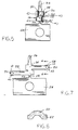
- an electrical connector generally designated 10 which includes a dielectric housing, generally designated 12, for receiving a plurality of receptacle contacts or terminals, generally designated 14, which embody the concepts of the invention.
- Housing 12 includes a body 16 having a plurality of cavities 18 which receive terminals 14.
- a plurality of hollow pegs 20 project upwardly from body 16 for insertion through appropriate holes 22 in a printed circuit board 24 to which the connector is mounted.
- an opening 28 in body 16, outside of each peg 20, is provided and through which a solder tail 26 (described hereinafter) of a respective terminal 14 extends through the respective hole 22 in circuit board 24.
- the solder tail is appropriately connected by soldering to circuit traces on side 30 of the circuit board or to through plating in the holes in the board.
- hollow pegs 20 project slightly beyond the side 30 of printed circuit board 24 opposite the side of the board to which body 16 is mounted.
- solder tails 26 projecting through the printed circuit board on the outside of hollow pegs 20, the solder tails are exposed exteriorly of the hollow pegs for soldering to circuit traces on the opposite side of the printed circuit board or to through plating in the holes in the board.
- the soldering may be carried out by conventional wave soldering techniques wherein a molten solder wave contacts the opposite side 30 of the printed circuit board to solder the solder tails to the circuit traces or hole plating.
- solder wave is sufficiently blocked from entering the distal ends of the pegs and into the cavities 18 in body 16 where the solder would, otherwise, contaminate the terminals within the cavities.
- Terminals 14 will be described in greater detail, but in the context of connector 10 in Figures 1-3, the terminals are designed for receiving contact pins (not shown) insertable into housing 12 from a mating or complementary connector either from the top of the connector 10, as shown by arrow "A" (Fig. 3) through a bore 32 in each peg 20, or from the bottom of the connector, in the direction of arrow "B", into contact with a terminal disposed within the respective cavity in the housing.
- arrow "A" Fig. 3
- a bore 32 in each peg 20 or from the bottom of the connector, in the direction of arrow "B"
- each terminal 14 includes a generally flat base 34 from which solder tail 26 extends in a coplanar manner.
- the terminal includes a pair of generally U-shaped members, generally designated 36, which combine to define a contact pin receiving opening 38 (Fig. 4).
- Each U-shaped member 36 includes a first leg 40 fixed to and projecting generally perpendicularly from base 34, a second or free leg 42 projecting back toward base 34, and a bight portion 44 joining legs 40,42. It can be seen in Figure 5 that U-shaped members 36 are spaced longitudinally of the terminal (i.e., longitudinally of opening 38 and solder tail portion 26) and are reversed in orientation. To this end, it can be seen that the first legs 40 are disposed laterally outwardly of the second legs 42 of the other U-shaped members. This lateral spacing or disposition allows for flexing of free legs 42 when a contact pin is inserted into opening 38.
- leg 42 of each U-shaped member 36 is provided with an inwardly projecting contact detent or dimple 50 which establishes engagement and electrical contact with a mating terminal pin inserted into opening 38.
- Figure 5 shows base 34 of terminal 14 connected by a web 52 to a strip 54 of a metal blank from which the terminal is stamped and formed. This is shown in Figure 5 simply for illustration purposes.
- Line 56 represents a score line at which the terminal is severed for insertion into a respective cavity 18 of housing 12.
- Figure 7 shows the components of terminal 14 after having been stamped from a continuous metal blank and with contact detents 50 stamped into distal ends of longitudinally running strips 58 of the blank. Each strip 58 subsequently is formed into the U-shaped members 36 described above.
- Base 34 and coplanar solder tail 26 are shown in Figure 7 as having been stamped from the metal blank into the ultimate shapes thereof in the stamped and formed terminal described above in relation to Figures 4 and 5.
- an electrical terminal 14 has been provided to define a contact pin-receiving receptacle.
- the terminal with U-shaped members 36, provides a very low profile (i.e., longitudinally of the terminal) to facilitate the provision of a very low profile connector 10.
- the terminal and the connector can be mated with a complementary connector or header from either the top or bottom thereof. Free legs 42 of the U-shaped members provide for high pressure contact reliability, and formed portion 43 of the U-shaped members provide anti-overstress protection for the terminal when a pin is inserted thereinto through opening 38.
Landscapes
- Engineering & Computer Science (AREA)
- Manufacturing & Machinery (AREA)
- Microelectronics & Electronic Packaging (AREA)
- Coupling Device And Connection With Printed Circuit (AREA)
- Multi-Conductor Connections (AREA)
Claims (7)
- Elektrischer Steckverbinder (10), der auf der Vorderseite einer mit mehreren Löchern (22) versehenen Leiterplatte (24) anbringbar ist und ein isolierendes Gehäuse (12) mit einem Hauptteil (16) umfaßt, das mit mehreren Kammern (18) zur jeweiligen Aufnahme einer elektrischen Klemme (14) versehen ist, wobei ein Klemmenteil (26) mit einer Leiterbahn auf der Leiterplatte verbunden ist, wobei ferner die Kammern zu den zugehörigen Löchern (22) ausgerichtet sind und mit diesen in Verbindung stehen, so daß eine Gegenklemme durch das betreffende Loch (22) in die Kammer (18) einführbar ist, um mit einer elektrischen Klemme (14) einen Kontakt herzustellen, wobei das Gehäuse (12) so positionierbar ist, daß die Leiterplatte (24) und das Gehäuse (12) im großen und ganzen benachbart zueinander angeordnet sind, und wobei von dem Gehäuse (12) mehrere Lötmaskenzapfen (20) so vorstehen, daß sie in die Löcher (22) einführbar sind, damit beim Verlöten der elektrischen Klemmen mit den Leiterbahnen der Leiterplatte (24) kein Lötmittel in die Löcher eindringt,
dadurch gekennzeichnet,
daß die Zapfen (20) hohl ausgebildet sind, und daß das Zapfeninnere (32) beim Anbringen des Gehäuses (12) an der Leiterplatte (24) jeweils zu einem zugeordneten Loch (18) ausgerichtet ist, und so mit diesem in Verbindung steht, daß die Gegenklemmen durch die hohlen Zapfen (20) eingeführt und in Kontakt mit den Klemmen (14) im Inneren des Gehäuses gebracht werden können. - Elektrischer Steckverbinder nach Anspruch 1, bei dem die hohl ausgebildeten Zapfen über die Vorderseite der Leiterplatte vorsteht.
- Elektrischer Steckverbinder nach Anspruch 1 oder 2, bei dem das Gehäuse (12) außerhalb des Zapfens (20) eine Öffnung (28) umfaßt, durch die eine Lötfahne (26) der elektrischen Klemme (14) vorsteht.
- Elektrischer Steckverbinder nach Anspruch 1, 2 oder 3, bei dem das Gehäuse (12) so gestaltet ist, daß die Gegenklemmen entweder durch die Leiterplatte oder von der gegenüberliegenden Seite aus in das Gehäuse einführbar sind, um einen Kontakt mit den Klemmen herzustellen.
- Elektrischer Steckverbinder nach Anspruch 1, bei dem die elektrische Klemme ein Basisteil (34) und zwei U-förmige Teile (36) umfaßt, die eine Aufnahmeöffnung für einen Kontakt- oder Steckerstift bilden, wobei bei den U-förmigen Teilen jeweils ein Schenkel (40) an dem Basisteil befestigt ist, daß er von diesem vorsteht, während der andere Schenkel (42) jeweils frei ist und in Richtung auf das Basisteil nach hinten vorsteht, und wobei die U-förmigen Teile in Längsrichtung der Öffnung zueinander beabstandet und umgekehrt zueinander ausgerichtet sind.
- Elektrischer Steckverbinder nach Anspruch 1, bei dem die hohlen Zapfen (20) jeweils so bemessen sind, daß sie näherungsweise in etwa den gleichen Durchmesser aufweisen# wie die zugehörigen Gegenlöcher (22) in der Leiterplatte (24).
- Elektrischer Steckverbinder nach Anspruch 1, bei dem das Gehäuse (12) mit dem Hauptteil (16) und den hohlen Zapfen (20) aus einem einstückig geformten oder gegossenen dielektrischen Material besteht.
Applications Claiming Priority (2)
| Application Number | Priority Date | Filing Date | Title |
|---|---|---|---|
| US61551190A | 1990-11-19 | 1990-11-19 | |
| US615511 | 1990-11-19 |
Publications (3)
| Publication Number | Publication Date |
|---|---|
| EP0486845A2 EP0486845A2 (de) | 1992-05-27 |
| EP0486845A3 EP0486845A3 (en) | 1993-04-14 |
| EP0486845B1 true EP0486845B1 (de) | 1996-08-28 |
Family
ID=24465711
Family Applications (1)
| Application Number | Title | Priority Date | Filing Date |
|---|---|---|---|
| EP91118300A Expired - Lifetime EP0486845B1 (de) | 1990-11-19 | 1991-10-26 | Elektrischer Verbinder mit Lötmaske |
Country Status (5)
| Country | Link |
|---|---|
| EP (1) | EP0486845B1 (de) |
| JP (1) | JPH069148B2 (de) |
| KR (1) | KR960002134B1 (de) |
| DE (1) | DE69121674T2 (de) |
| SG (1) | SG44634A1 (de) |
Families Citing this family (1)
| Publication number | Priority date | Publication date | Assignee | Title |
|---|---|---|---|---|
| US5538448A (en) * | 1993-09-10 | 1996-07-23 | Tsao; Jenn | Gang modular jack |
Family Cites Families (7)
| Publication number | Priority date | Publication date | Assignee | Title |
|---|---|---|---|---|
| US3222632A (en) * | 1964-06-08 | 1965-12-07 | Amp Inc | Pin and socket connector assembly adapted for solder connection |
| US3673551A (en) * | 1969-11-28 | 1972-06-27 | Molex Products Co | Integrated circuit terminal and method |
| US4010992A (en) * | 1976-01-08 | 1977-03-08 | Aries Electronics, Inc. | Low profile socket having terminal pins sealingly mounted in socket housing |
| US4114008A (en) * | 1976-06-14 | 1978-09-12 | Teltec, Incorporated | Relay seal cap |
| US4466684A (en) * | 1981-12-17 | 1984-08-21 | Texas Instruments Incorporated | Low insertion force connector |
| JPH046134Y2 (de) * | 1987-02-26 | 1992-02-20 | ||
| US4750889A (en) * | 1987-02-27 | 1988-06-14 | Minnesota Mining & Manufacturing Company | Through-board electrical component header having integral solder mask |
-
1991
- 1991-10-26 EP EP91118300A patent/EP0486845B1/de not_active Expired - Lifetime
- 1991-10-26 SG SG1996004631A patent/SG44634A1/en unknown
- 1991-10-26 DE DE69121674T patent/DE69121674T2/de not_active Expired - Fee Related
- 1991-11-18 JP JP3329481A patent/JPH069148B2/ja not_active Expired - Lifetime
- 1991-11-18 KR KR1019910020484A patent/KR960002134B1/ko not_active Expired - Fee Related
Also Published As
| Publication number | Publication date |
|---|---|
| SG44634A1 (en) | 1997-12-19 |
| EP0486845A3 (en) | 1993-04-14 |
| DE69121674D1 (de) | 1996-10-02 |
| KR920010990A (ko) | 1992-06-27 |
| EP0486845A2 (de) | 1992-05-27 |
| JPH069148B2 (ja) | 1994-02-02 |
| JPH04301380A (ja) | 1992-10-23 |
| KR960002134B1 (ko) | 1996-02-10 |
| DE69121674T2 (de) | 1997-01-23 |
Similar Documents
| Publication | Publication Date | Title |
|---|---|---|
| US6071152A (en) | Electrical connector with inserted terminals | |
| US4715820A (en) | Connection system for printed circuit boards | |
| EP0795929B1 (de) | Elektrische Verbinderanordnung mit verbessertem Haltemittel | |
| US6296496B1 (en) | Electrical connector and method for attaching the same to a printed circuit board | |
| JP2617159B2 (ja) | 薄型電気コネクタ | |
| EP0449570B1 (de) | Mehrstiftiger elektrischer Verbinder mit Anschlussstiften | |
| US5667392A (en) | Electrical connector with stabilized contact | |
| CA1169511A (en) | Cover for multiple terminal electrical connector | |
| KR970004145B1 (ko) | 향상된 단자 보유 수단을 갖는 전기 커넥터 | |
| EP0543278B1 (de) | Elektrischer Flachbauverbinder | |
| US3697933A (en) | Connector block | |
| US4428633A (en) | Dual-in-line socket assembly | |
| EP0657960B1 (de) | Leiterplattenverbinder | |
| US5876237A (en) | Electrical connector | |
| US6135785A (en) | Small pitch electrical connector having narrowed portion | |
| EP0280508B1 (de) | Endstück eines eine Platte durchdringenden, elektrischen Bauelementes mit eingebauter Lötmaske | |
| EP0856922B1 (de) | Leiterplattenverbinder mit Gabelmontage | |
| EP0068656B1 (de) | Elektrischer Anschlusskontakt mit Hohlraumausgleichmittel | |
| EP0639871A2 (de) | Oberflächenmontierbarer elektrischer Verbinder und Kontaktklemme dazu | |
| EP0717473B1 (de) | Elektrisches Stiftfeld auf einer Leiterplatte | |
| US6077087A (en) | Coaxial connector module with an overmolded ground contact | |
| US5178564A (en) | Electrical connector with solder mask | |
| EP0109297B1 (de) | Elektrische Kontaktorgane und Zusammenbau elektrischer Verbinder | |
| JP3898643B2 (ja) | 小型基板対基板コネクタ | |
| EP0486845B1 (de) | Elektrischer Verbinder mit Lötmaske |
Legal Events
| Date | Code | Title | Description |
|---|---|---|---|
| PUAI | Public reference made under article 153(3) epc to a published international application that has entered the european phase |
Free format text: ORIGINAL CODE: 0009012 |
|
| AK | Designated contracting states |
Kind code of ref document: A2 Designated state(s): DE FR GB |
|
| PUAL | Search report despatched |
Free format text: ORIGINAL CODE: 0009013 |
|
| AK | Designated contracting states |
Kind code of ref document: A3 Designated state(s): DE FR GB |
|
| 17P | Request for examination filed |
Effective date: 19930922 |
|
| 17Q | First examination report despatched |
Effective date: 19940812 |
|
| GRAH | Despatch of communication of intention to grant a patent |
Free format text: ORIGINAL CODE: EPIDOS IGRA |
|
| GRAH | Despatch of communication of intention to grant a patent |
Free format text: ORIGINAL CODE: EPIDOS IGRA |
|
| GRAA | (expected) grant |
Free format text: ORIGINAL CODE: 0009210 |
|
| AK | Designated contracting states |
Kind code of ref document: B1 Designated state(s): DE FR GB |
|
| ET | Fr: translation filed | ||
| REF | Corresponds to: |
Ref document number: 69121674 Country of ref document: DE Date of ref document: 19961002 |
|
| PLBE | No opposition filed within time limit |
Free format text: ORIGINAL CODE: 0009261 |
|
| STAA | Information on the status of an ep patent application or granted ep patent |
Free format text: STATUS: NO OPPOSITION FILED WITHIN TIME LIMIT |
|
| 26N | No opposition filed | ||
| PGFP | Annual fee paid to national office [announced via postgrant information from national office to epo] |
Ref country code: GB Payment date: 19990913 Year of fee payment: 9 |
|
| PGFP | Annual fee paid to national office [announced via postgrant information from national office to epo] |
Ref country code: FR Payment date: 19991013 Year of fee payment: 9 |
|
| PGFP | Annual fee paid to national office [announced via postgrant information from national office to epo] |
Ref country code: DE Payment date: 19991027 Year of fee payment: 9 |
|
| PG25 | Lapsed in a contracting state [announced via postgrant information from national office to epo] |
Ref country code: GB Free format text: LAPSE BECAUSE OF NON-PAYMENT OF DUE FEES Effective date: 20001026 |
|
| GBPC | Gb: european patent ceased through non-payment of renewal fee |
Effective date: 20001026 |
|
| PG25 | Lapsed in a contracting state [announced via postgrant information from national office to epo] |
Ref country code: FR Free format text: LAPSE BECAUSE OF NON-PAYMENT OF DUE FEES Effective date: 20010629 |
|
| PG25 | Lapsed in a contracting state [announced via postgrant information from national office to epo] |
Ref country code: DE Free format text: LAPSE BECAUSE OF NON-PAYMENT OF DUE FEES Effective date: 20010703 |
|
| REG | Reference to a national code |
Ref country code: FR Ref legal event code: ST |