EP0485918A2 - Verfahren und Gerät zum digitalen Schalten von FM-Signalen mit geringem Übersprechen - Google Patents
Verfahren und Gerät zum digitalen Schalten von FM-Signalen mit geringem Übersprechen Download PDFInfo
- Publication number
- EP0485918A2 EP0485918A2 EP91119162A EP91119162A EP0485918A2 EP 0485918 A2 EP0485918 A2 EP 0485918A2 EP 91119162 A EP91119162 A EP 91119162A EP 91119162 A EP91119162 A EP 91119162A EP 0485918 A2 EP0485918 A2 EP 0485918A2
- Authority
- EP
- European Patent Office
- Prior art keywords
- switching
- dummy
- output
- digital
- frequency
- Prior art date
- Legal status (The legal status is an assumption and is not a legal conclusion. Google has not performed a legal analysis and makes no representation as to the accuracy of the status listed.)
- Withdrawn
Links
Images

Classifications
-
- H—ELECTRICITY
- H03—ELECTRONIC CIRCUITRY
- H03K—PULSE TECHNIQUE
- H03K17/00—Electronic switching or gating, i.e. not by contact-making and –breaking
- H03K17/16—Modifications for eliminating interference voltages or currents
- H03K17/161—Modifications for eliminating interference voltages or currents in field-effect transistor switches
- H03K17/162—Modifications for eliminating interference voltages or currents in field-effect transistor switches without feedback from the output circuit to the control circuit
-
- H—ELECTRICITY
- H03—ELECTRONIC CIRCUITRY
- H03K—PULSE TECHNIQUE
- H03K17/00—Electronic switching or gating, i.e. not by contact-making and –breaking
- H03K17/51—Electronic switching or gating, i.e. not by contact-making and –breaking characterised by the components used
- H03K17/56—Electronic switching or gating, i.e. not by contact-making and –breaking characterised by the components used by the use, as active elements, of semiconductor devices
- H03K17/687—Electronic switching or gating, i.e. not by contact-making and –breaking characterised by the components used by the use, as active elements, of semiconductor devices the devices being field-effect transistors
- H03K17/693—Switching arrangements with several input- or output-terminals, e.g. multiplexers, distributors
Definitions
- This invention relates to digital switching apparatus including multiple digital switching circuits and, more particularly, to methods andapparatus for reducing crosstalk between the switching circuits.
- the invention is particularly useful in reducing crosstalk in digital switching apparatus which receives EM input signals.
- a digital switch as used in telecommunication systems, consists of a plurality of digital switching circuits in an integrated circuit. Signals applied to the inputs of the digital switch are routed to selected outputs in response to control signals.
- Digital switches can be used to switch frequency modulated (EM) video information.
- An analog EM signal is applied directly to an input of the digital switch. Since the switching path within the digital switch includes multiple cascaded digital gates, the analog EM signal is clipped on the positive and negative peaks of the sine wave signal.
- the output of the switch is a square wave signal having a period which varies in accordance with the input analog EM signal. After filtering of the digital switch output, the analog EM input signal is reproduced.
- crosstalk results from capacitive coupling between inputs and outputs and from inductive coupling between outputs.
- the inductive coupling between outputs is caused by stray inductance in the supply voltage and ground lines and can contribute over 90% of the total crosstalk. Reduction of crosstalk caused by inductive coupling would produce a major improvement in FM switching.
- the apparatus comprises a plurality of functional switching circuits, each having an input for receiving an FM signal at a first frequency and each generating first switching transients in response to the FM signal, means for generating second switching transients in response to the FM signal, the second switching transients being shifted in phase relative to the first switching transients such that a crosstalk signal resulting from the first and second switching transients has a frequency of twice the first frequency, and filter means associated with the functional switching circuits for attenuating the crosstalk signal.
- the means for generating second switching transients preferably comprises a plurality of dummy switching circuits, one corresponding to each of the functional switching circuits, each dummy switching circuit being connected such that its output is a digital inversion of the output of the corresponding functional switching circuit.
- each of the functional switching circuits and each of the dummy switching circuits includes a capacitively loaded MOS output stage.
- Each of the dummy switching circuits includes inverting means so that the output of each dummy switching circuit is opposite in phase from the output of the corresponding functional switching circuit.
- the functional switching circuits and the dummy switching circuits are typically located on an integrated circuit.
- a capacitive load for each of the dummy switching circuits can be located external to the integrated circuit. In this case, a connector pin is required for each dummy switching circuit.
- the capacitive load for each of the dummy switching circuits can be located on the integrated circuit. In this case, the capacitive loads are externally connected through a common connector pin of the integrated circuit.
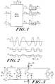
- FIG. 1 A block diagram of apparatus for digital switching of FM signals is shown in FIG. 1.
- An integrated circuit digital switch 10 includes inputs 121, 122, ---12 n , outputs 141, 142,---14 m and select lines 16. An input signal applied to one of the inputs 12 is switched to one of the outputs 14 under control of select lines 16.
- the digital switch 10 includes gating circuitry to perform the required switching.
- the outputs 14 of digital switch 10 are connected through filters 20 to provide filter outputs 241, 242, ---24 m .
- An example of a digital switch 10 has 64 inputs and 16 outputs.
- the digital switch is configured as 16 parallel circuit modules, each capable of switching one of the 64 inputs to its output.
- Each circuit module requires 6 control bits, for a total of 96 (16x16) control bits.
- the control bits are transferred into the digital switch serially and are stored.
- the 64 x 16 digital switch is described in more detail in European application S.N. 90 104724.1.
- An example of an analog FM signal 28 is shown in FIG. 2.
- the FM signal 28 applied to input 121 of the digital switch it is clipped by the cascaded digital stages within digital switch 10.
- An output signal 30 appearing on output 14 m of the digital switch is a square wave voltage having a period which varies in accordance with the FM signal 28.
- An output signal 32 on filter output 24 m is a reproduction of the input FM signal 28.
- FIG. 3 A schematic diagram of the output stages of the digital switch 10 is shown in FIG. 3.
- An output stage 38 including a PMOS transistor 40 and an NMOS transistor 42 connected in series, drives a load represented by a capacitor 44.
- the drain of the PMOS transistor 40 is connected to an on-chip voltage supply line 46, and the source of the NMOS transistor is connected to an on-chip ground line 48.
- the source of transistor 40 and the drain of transistor 42 are connected to output 14.
- Additional output stages for driving outputs 14 2--- , 14 m are connected to supply line 46 and ground line 48.
- the connection between on-chip supply 46 and a positive supply voltage is represented by an inductance 50.
- the connection between the on-chip ground line 48 and the system ground is represented by an inductance 52.
- Inductances 50 and 42 represent stray inductance in the connecting lines.
- the capacitor 44 represents a capacitive load on output 141 of the digital switch 10. Since the capacitor 44 is external to the digital switch chip, it is connected directly to the system ground rather than to the on-chip ground line 48.
- a transient current passes through inductance 50 or inductance 52.
- the transient current through inductance 50 causes a voltage spike on supply line 46.
- a transient current through inductance 52 causes a voltage spike on ground line 48.
- Output signal 60 shown in FIG. 5 appears on output 141 of the digital output stage 38 shown in FIG. 4.
- transistor 40 When output 141 switches from 0 volts to +5 volts, transistor 40 is on and transistor 42 is off.
- a transient current I p flows through inductance 50 and transistor 40 for charging of capacitor 44.
- the transient current I p as illustrated by waveform 62 of FIG. 5, induces a voltage spike across inductance 50.
- output 141 switches from +5 volts to 0 volts, transistor 40 is off and transistor 42 is on.
- a transient current I n flows through transistor 42 and inductance 52 for discharging of capacitor 44.
- the transient current I n induces a voltage spike across the inductance 52.
- the transient current I p produces voltage spikes on the on-chip supply line 46.
- the transient current I n produces voltage spikes on the on-chip ground line 48.
- the transient voltages on supply line 46 and ground line 48 produce voltage spikes on the other output stages connected to on-chip supply line 46 and on-chip ground line 48.
- any voltage spikes on supply line 46 are coupled directly to output 142.
- transistor 43 of the second output stage is on, any voltage spikes on ground line 48 are coupled directly to output 142. Coupling of voltage spikes occurs in the same way on all output stages of the digital switch.
- the switching of transistors 40 and 42 produces crosstalk on other outputs of the digital switch.
- the magnitude of the crosstalk is directly proportional to the number of outputs that are switching simultaneously.
- the inductive crosstalk per switched output is about 100 millivolts, thereby resulting in a total crosstalk of 1.5 volts for 15 simultaneously switched outputs.
- transient current I p and transient current I n each have a fundamental frequency that is the same as the fundamental frequency of output signal 60. Since the crosstalk and the signals have the same fundamental frequency, the transients can not be filtered.
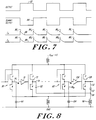
- FIG. 6 A circuit in accordance with the present invention is shown in FIG. 6. Corresponding waveforms are shown in FIG. 7.
- the output stage 38 including transistors 40 and 42 connected to output 141, is the same as the output stage 3B shown in FIG. 4 and described hereinabove.
- the input signal to transistors 40 and 42 is connected to the input of a digital inverter 70.
- the output of inverter 70 is connected to the input of a dummy output stage 72, including a PMOS transistor 74 and an NMOS transistor 76 connected in series between on-chip supply line 46 and on-chip ground line 48.
- the output of inverter 70 is connected to the gates of transistors 74 and 76.
- the drain of transistor 74 is connected to on-chip supply line 46, and the source of transistor 76 is connected to on-chip ground line 48.
- the source of transistor 74 and the drain of transistor 76 are connected to a dummy output 78.
- a capacitor 80 typically located external to the chip, is connected between dummy output 78 and the system ground.
- transistors 40 and 74 are identical or nearly identical, and transistors 42 and 76 are identical or nearly identical so that the dummy output stage 72 operates in the same manner as the output stage 38 of the digital switch 10.
- the capacitors 44 and 80 are equal or nearly equal in value.
- the inverter 70 and the dummy output stage 72 constitute a dummy switching circuit 81 which provides a nonfunctional dummy output.
- the output stage 38 is a functional part of the digital switch 10.
- a dummy switching circuit is provided for each output stage of the digital switch.
- each output stage has a corresponding dummy switching circuit for reducing crosstalk as described below.
- the purpose of the dummy switching circuit 81 is to produce transients which are substantially identical to the transients produced by the output stage 38, but displaced in time.
- waveform 82 represents an output signal on output 141 of the output stage 38
- waveform 84 represents the corresponding signal on dummy output 78.
- Waveforms 82 and 84 are inverted, or out of phase, relative to each other.
- the transients generated by output stage 38 and dummy switching circuit 81 add, thereby producing the waveforms 86 and 88 shown in FIG. 7.
- Waveform 86 represents the transient current I p through inductance 50
- waveform 88 represents the transient current I n through inductance 52
- Transients 861 of current I p are produced by the positive-going edges of waveform 82 on output 141, when transistor 40 turns on and charges capacitor 44 through inductance 50.
- Transients 862 of current I p are produced by the positive-going edges of waveform 84 on dummy output 78, when transistor 74 turns on and charges capacitor 80 through inductance 50. Since the currents for transistors 40 and 74 are both drawn through inductance 50, the transients add and produce waveform 86.
- Transients 881 of current I n are produced by the negative-going edges of waveform 84 on dummy output 78, when transistor 76 turns on and discharges capacitor 80 through inductance 52.
- transients 882 of current I n are produced by the negative-going edges of waveform 82 on output 141, when transistor 42 turns on and discharges capacitor 44 through inductance 52. Since the currents for transistors 42 and 76 both pass through inductance 52, the transients add and produce waveform 88.
- the fundamental frequency component of transient currents I p and I n is twice the fundamental frequency of the output signal 82.
- the lowest frequency component of the crosstalk resulting from transient currents I p and I n is twice the frequency of the FM signal.
- the crosstalk can be removed with a bandpass filter which allows the desired FM signal of frequency f ⁇ f to pass, where f is the carrier frequency and ⁇ f is the frequency deviation.
- the frequency components of the crosstalk are 2f ⁇ 2 ⁇ f or higher and are attenuated by the bandpass filter.
- all FM input signals to the digital switch 10 should have approximately the same carrier frequency. In normal practice, this requirement is met.
- the crosstalk which appears in the outputs of digital switch 10 at twice the FM carrier frequency can be filtered by filters 20 as shown in FIG. 1.
- the digital switch typically has a frequency response which will attenuate crosstalk at twice the FM signal frequency. This filtering results from the inherent frequency response of the digital switch. In general, filtering of crosstalk at twice the FM signal frequency can be performed at any convenient location in the apparatus.
- output 141 and dummy output 78 should make transitions at the same time. This can be achieved by building delay into output stage 38 to compensate for the delay produced by inverter 70. The delay can be achieved by a small resistor-capacitor circuit at the input to transistors 40 and 42. In practice, the FM signal passes through many digital stages in digital switch 10 before reaching output 141 so that the required delay can be inserted at any convenient location in the circuit after the connection of the inverter 70. As indicated above, the value of capacitor 80 should be equal to the capacitor 44. In cases where capacitor 44 is the stub of a transmission line, the value of capacitor 80 is made to approximate the effective capacitance of the transmission line stub.
- a dummy switching circuit 81 including inverter 70 and dummy output stage 72, is provided for each output stage of the digital switch 10.
- a dummy switching circuit corresponds to each functional output circuit of the digital switch 10.
- each dummy output is connected to a capacitor which is located external to the integrated circuit. This configuration requires one additional connector pin for each output of the digital switch 10, thereby increasing the number of connector pins by 16 for a 16 output switch.
- Output stage 38 of the digital switch 10 has output 141 connected to external capacitor 44 as shown in FIG. 6.
- Output 78 of dummy output stage 72 is connected through an on-chip capacitor 92 to a connector pin 94.
- the connector pin 94 is externally connected to the system ground by a connection through inductance 96.
- Inductance 96 represents stray inductance in the connecting line.
- Another output stage 102 of the digital switch 10 has output 14 m connected to an external capacitor 104. The input of stage 102 is connected through an inverter 106 to a dummy output stage 108.
- the dummy output stage 108 has a dummy output 110 connected through an on-chip capacitor 112 to connector pin 94.
- the circuit including output stage 102, inverter 106 and dummy output stage 108 is the same as the circuit including output stage 38, inverter 70 and dummy output stage 72. This combination of circuits is repeated for each output of the digital switch 10.
- Each dummy output is connected through a separate on-chip capacitor to connector pin 94.
- each of the on-chip capacitors 92, 112, etc. should be equal to the average equivalent capacitance of the output loads. In the configuration of FIG. 8, only one additional connector pin 94 is required to implement the crosstalk reduction scheme for a multiple output digital switch 10.
Landscapes
- Electronic Switches (AREA)
- Use Of Switch Circuits For Exchanges And Methods Of Control Of Multiplex Exchanges (AREA)
Applications Claiming Priority (2)
| Application Number | Priority Date | Filing Date | Title |
|---|---|---|---|
| US613177 | 1990-11-14 | ||
| US07/613,177 US5204982A (en) | 1990-11-14 | 1990-11-14 | Method and apparatus for digital switching of fm signals with reduced crosstalk |
Publications (2)
| Publication Number | Publication Date |
|---|---|
| EP0485918A2 true EP0485918A2 (de) | 1992-05-20 |
| EP0485918A3 EP0485918A3 (en) | 1992-07-01 |
Family
ID=24456188
Family Applications (1)
| Application Number | Title | Priority Date | Filing Date |
|---|---|---|---|
| EP19910119162 Withdrawn EP0485918A3 (en) | 1990-11-14 | 1991-11-11 | Method and apparatus for digital switching of fm signals with reduced crosstalk |
Country Status (4)
| Country | Link |
|---|---|
| US (1) | US5204982A (de) |
| EP (1) | EP0485918A3 (de) |
| JP (1) | JPH04286498A (de) |
| CA (1) | CA2055398A1 (de) |
Cited By (2)
| Publication number | Priority date | Publication date | Assignee | Title |
|---|---|---|---|---|
| WO2003043192A1 (de) * | 2001-11-12 | 2003-05-22 | Infineon Technologies Ag | Verfahren zur vermeidung von transienten bei schaltvorgängen in integrierten schaltkreisen sowie integrierter schaltkreis |
| EP1679797A1 (de) * | 2004-12-31 | 2006-07-12 | STMicroelectronics Pvt. Ltd | Schnelle Ausgangspufferschaltung mit niedriger Störspannung |
Families Citing this family (4)
| Publication number | Priority date | Publication date | Assignee | Title |
|---|---|---|---|---|
| US5649160A (en) * | 1995-05-23 | 1997-07-15 | Microunity Systems Engineering, Inc. | Noise reduction in integrated circuits and circuit assemblies |
| US5565804A (en) * | 1995-06-30 | 1996-10-15 | Acer Peripherals, Inc. | Signal switching circuit |
| CA2282882C (en) | 1998-09-22 | 2005-11-01 | Kabushiki Kaisha Toshiba | Serial transmission path switching system |
| US6794924B2 (en) * | 2001-05-24 | 2004-09-21 | Intersil Corporation | Apparatus and method for minimizing spurious harmonic noise in switched current steering architectures |
Family Cites Families (6)
| Publication number | Priority date | Publication date | Assignee | Title |
|---|---|---|---|---|
| FR2047179A5 (de) * | 1969-04-30 | 1971-03-12 | Solartron Electronic Group | |
| GB1276741A (en) * | 1969-04-30 | 1972-06-07 | Solartron Electronic Group | Improvements in or relating to electronic switches |
| CA1255005A (en) * | 1978-04-11 | 1989-05-30 | Noel O. Fothergill | Narrow band correlator and noise cancellor |
| JPS58187015A (ja) * | 1982-04-26 | 1983-11-01 | Nippon Telegr & Teleph Corp <Ntt> | スイツチト・キヤパシタ回路 |
| EP0269758B1 (de) * | 1986-12-01 | 1991-01-23 | Deutsche ITT Industries GmbH | Stromumschalter |
| US4752703A (en) * | 1987-04-23 | 1988-06-21 | Industrial Technology Research Institute | Current source polarity switching circuit |
-
1990
- 1990-11-14 US US07/613,177 patent/US5204982A/en not_active Expired - Lifetime
-
1991
- 1991-11-11 EP EP19910119162 patent/EP0485918A3/en not_active Withdrawn
- 1991-11-13 CA CA002055398A patent/CA2055398A1/en not_active Abandoned
- 1991-11-14 JP JP3325100A patent/JPH04286498A/ja not_active Withdrawn
Cited By (3)
| Publication number | Priority date | Publication date | Assignee | Title |
|---|---|---|---|---|
| WO2003043192A1 (de) * | 2001-11-12 | 2003-05-22 | Infineon Technologies Ag | Verfahren zur vermeidung von transienten bei schaltvorgängen in integrierten schaltkreisen sowie integrierter schaltkreis |
| US7129737B2 (en) | 2001-11-12 | 2006-10-31 | Infineon Technologies Ag | Method for avoiding transients during switching processes in integrated circuits, and an integrated circuit |
| EP1679797A1 (de) * | 2004-12-31 | 2006-07-12 | STMicroelectronics Pvt. Ltd | Schnelle Ausgangspufferschaltung mit niedriger Störspannung |
Also Published As
| Publication number | Publication date |
|---|---|
| CA2055398A1 (en) | 1992-05-15 |
| US5204982A (en) | 1993-04-20 |
| JPH04286498A (ja) | 1992-10-12 |
| EP0485918A3 (en) | 1992-07-01 |
Similar Documents
| Publication | Publication Date | Title |
|---|---|---|
| EP0646854B1 (de) | Schaltung zur Verteilung des Hochfrequenz-Taktsignals mit reduzierter Taktverschiebung | |
| DE69122189T2 (de) | Flip-Flop-Schaltung vom "Master-Slave"-Typ | |
| US5644257A (en) | Sampling circuit charge management | |
| US6452442B1 (en) | Apparatus for obtaining noise immunity in electrical circuits | |
| US5051882A (en) | Three reservoir capacitor charge pump circuit | |
| EP0633662B1 (de) | Schaltungsanordnung für einen Ringoszillator | |
| DE3050199T1 (de) | Dynamic ratioless circuitry for random logic applications | |
| US4994774A (en) | Integrated low-pass filter arrangement | |
| EP0678980A1 (de) | Verzerrungsarme Schaltung mit geschalteten Kapazitäten | |
| US5204982A (en) | Method and apparatus for digital switching of fm signals with reduced crosstalk | |
| US5644262A (en) | Digitally controlled capacitive load | |
| US5144161A (en) | Logic circuit for switching noise reduction | |
| US4376251A (en) | Waveform shaping circuit | |
| DE4140686B4 (de) | Signalverarbeitungssystem | |
| US5708372A (en) | Semiconductor device with electromagnetic radiation reduced | |
| US4743872A (en) | Switched capacitor circuit | |
| DE10357785B3 (de) | SC-Schaltungsanordnung | |
| US3069567A (en) | Radio-frequency transistor gate apparatus | |
| US4508982A (en) | Floating node stabilizing circuit for a switched-capacitor circuit and filter | |
| US3725790A (en) | Shift register clock pulse distribution system | |
| EP1317793B1 (de) | Ladungspumpenschaltung | |
| CA1206542A (en) | Switched capacitor high-pass filter | |
| US4563660A (en) | Noise isolation system for high-speed circuits | |
| EP1033814B1 (de) | Integrierte Schaltung zur Erzeugung zweier Ausgangstakte mit zeitlich nicht überlappenden Pegeln | |
| US7098719B2 (en) | Multiplexer with clock suppression |
Legal Events
| Date | Code | Title | Description |
|---|---|---|---|
| PUAI | Public reference made under article 153(3) epc to a published international application that has entered the european phase |
Free format text: ORIGINAL CODE: 0009012 |
|
| PUAL | Search report despatched |
Free format text: ORIGINAL CODE: 0009013 |
|
| AK | Designated contracting states |
Kind code of ref document: A2 Designated state(s): BE DE FR GB IT |
|
| AK | Designated contracting states |
Kind code of ref document: A3 Designated state(s): BE DE FR GB IT |
|
| 17P | Request for examination filed |
Effective date: 19921228 |
|
| STAA | Information on the status of an ep patent application or granted ep patent |
Free format text: STATUS: THE APPLICATION IS DEEMED TO BE WITHDRAWN |
|
| 18D | Application deemed to be withdrawn |
Effective date: 19950601 |