EP0484450B1 - Fasermodulatoren - Google Patents
Fasermodulatoren Download PDFInfo
- Publication number
- EP0484450B1 EP0484450B1 EP90912652A EP90912652A EP0484450B1 EP 0484450 B1 EP0484450 B1 EP 0484450B1 EP 90912652 A EP90912652 A EP 90912652A EP 90912652 A EP90912652 A EP 90912652A EP 0484450 B1 EP0484450 B1 EP 0484450B1
- Authority
- EP
- European Patent Office
- Prior art keywords
- tapered portion
- fibre
- modulator
- optical
- coupler
- Prior art date
- Legal status (The legal status is an assumption and is not a legal conclusion. Google has not performed a legal analysis and makes no representation as to the accuracy of the status listed.)
- Expired - Lifetime
Links
Images
Classifications
-
- G—PHYSICS
- G02—OPTICS
- G02F—OPTICAL DEVICES OR ARRANGEMENTS FOR THE CONTROL OF LIGHT BY MODIFICATION OF THE OPTICAL PROPERTIES OF THE MEDIA OF THE ELEMENTS INVOLVED THEREIN; NON-LINEAR OPTICS; FREQUENCY-CHANGING OF LIGHT; OPTICAL LOGIC ELEMENTS; OPTICAL ANALOGUE/DIGITAL CONVERTERS
- G02F1/00—Devices or arrangements for the control of the intensity, colour, phase, polarisation or direction of light arriving from an independent light source, e.g. switching, gating or modulating; Non-linear optics
- G02F1/01—Devices or arrangements for the control of the intensity, colour, phase, polarisation or direction of light arriving from an independent light source, e.g. switching, gating or modulating; Non-linear optics for the control of the intensity, phase, polarisation or colour
- G02F1/0128—Devices or arrangements for the control of the intensity, colour, phase, polarisation or direction of light arriving from an independent light source, e.g. switching, gating or modulating; Non-linear optics for the control of the intensity, phase, polarisation or colour based on electro-mechanical, magneto-mechanical, elasto-optic effects
- G02F1/0131—Devices or arrangements for the control of the intensity, colour, phase, polarisation or direction of light arriving from an independent light source, e.g. switching, gating or modulating; Non-linear optics for the control of the intensity, phase, polarisation or colour based on electro-mechanical, magneto-mechanical, elasto-optic effects based on photo-elastic effects, e.g. mechanically induced birefringence
- G02F1/0134—Devices or arrangements for the control of the intensity, colour, phase, polarisation or direction of light arriving from an independent light source, e.g. switching, gating or modulating; Non-linear optics for the control of the intensity, phase, polarisation or colour based on electro-mechanical, magneto-mechanical, elasto-optic effects based on photo-elastic effects, e.g. mechanically induced birefringence in optical waveguides
Definitions
- This invention relates to modulation techniques for optical communication systems, and in particular to modulation of light guided in an optical fibre.
- a significant problem within an optical communication network is the provision of flexibility points at which expansion, or rearrangement, of the network can subsequently be made. For flexibility, it is desirable to maximise the number of potential coupling or tapping points. This is not possible if there is significant loss at the tapping points not utilised.
- the aim of the present invention is to provide in-fibre modulation, and also to provide low-loss potential tapping points.
- the present invention provides an optical signal modulator formed by an optical fibre assembly comprising an optical fibre for carrying an optical signal to be modulated, the optical fibre having a tapered portion suspended between two support members without any intermediate support, and means for applying a modulation signal perturbation directly to the suspended tapered portion to vary the percentage transmission through the fibre by distorting the waveguide geometry of the suspended tapered portion and thereby causing coupling of the modes of the optical signal carried by the tapered portion into higher order bound modes in accordance with the modulation signal.
- the suspended tapered portion of the optical fibre is supported, under tension, between the two support members.
- the tapered portion comprises a fibre tapered by heating and drawing, the minimum radius of the tapered portion being 20 microns.
- the optical fibre assembly is constituted by two optical fibres fused together to form a fused fibre coupler.
- the perturbation applying means comprises a vibratile member, such as a piezo-electric device.
- the vibratile member may impart a lateral deformation, or changes in tension, to the tapered portion.
- the tapered portion may also be provided with an etched grating on its surface.
- the invention further provides a method of modulating, as defined in claim 14.
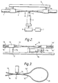
- Figure 1 shows an optical fibre 1 which carries an optical beam such as a CW laser beam.
- a suitable tapered portion 2 having an overall reduced diameter length of about 27mm, can be produced by heating and drawing a standard optical fibre at 1700°C.
- the insertion loss of such a tapered portion 2 is typically 0.05 dB.
- the supporting substrate 3 may be of any suitable material, but is preferably made of silica or some other material having a thermal expansion matched to that of the fibre 1.
- the tapered portion 2 of the fibre 1 is positioned adjacent to a modulation means that operates by deforming the tapered portion of the fibre by a greater or lesser extent causing a greater or lesser power loss from the fibre.
- the deformation is achieved by physical contact of a vibratile member 4 with the tapered portion 2 of the fibre 1 to produce a lateral deformation, but analagous lateral deformation could also be produced by electrostatic means.
- the vibratile member 4 is constituted by a pin mounted on a piezo-electric crystal 5, although alternative structures such as a shaped piezo-electric crystal could equally well be used.
- the piezo-electric crystal 5 is driven by a signal generator 6 that controls a variable voltage driver unit 7. For drive voltages of the order of 3 to 40 volts a longitudinal movement of the piezo-electric crystal 5 of typically 5 to 15 microns is obtained.
- the piezo-electric crystal 5 For efficient modulation, it is desirable to drive the piezo-electric crystal 5 so that it vibrates at, or close to, its resonant frequency.
- the frequency at which the piezo-electric crystal 5 resonates for a given material is dependent upon the piezo thickness and diameter.
- This resonant frequency is used, in a manner described below, as a carrier frequency for modulation with an information signal.
- the carrier (resonant) frequency for a piezo-electric crystal 5 can be varied slightly (by up to about 5 KHz) by varying the force of the vibratile member 4 against the fibre 1.
- An alternative modulation technique is to vary the frequency of the piezo-electric vibration, for example within + 5 KHz of the resonant frequency of the piezo-electric crystal 5. This may be done by frequency modulating the voltage oscillations of the driver unit 7. Both frequency modulation and amplitude modulation of the tapered portion 2 may be utilised simultaneously. Other modulation techniques may also be employed.
- Modulation in the tapered portion 2 of the fibre 1 is caused by the loss in this portion which results from deformation by the vibratile member 4. If we neglect the effect of the core of the tapered portion 2 of the fibre 1, it can be considered as strongly guided, multi-moded waveguide with a normalised frequency, V ⁇ 100, its bound modes being guided by the cladding-air interface. The taper is sufficiently slight that only the HE11 mode is excited.
- the fibre 1 is deformed laterally in order to provide a loss-modulated output signal. Longitudinal deformation, ie tension may also be utilised.
- the sensitising of the fibre 1 to the tension changes is preferably by way of a fibre coupler.
- Figure 2 illustrates a system utilising a fused or twisted fibre coupler, but an analagous technique can be applied to other sensitised fibres.
- a fused (or twisted and fused) fibre coupler 10 is mounted through silica channels 15 and between arms 11a attached to a substrate block 11.
- the fused coupler 10 is formed by fusing two optical fibres, these fibres being denoted by the reference numerals 13 and 14 on one side of the coupler, and by the reference numerals 13′ and 14′ on the other side of the coupler.
- the substrate block 11 incorporates a piezo-electric device 16 that is driven in a manner similar to that described with reference to Figure 1.
- the fused coupler 10 is fabricated under tension such that light is coupled straight through along the tapered portion 12 from the fibre 13 to the fibre 13′.
- a modification to the embodiment of Figure 2 is to provide a means for adjusting the basic tension of the coupler 10.
- couplers located in a transmission line at various access points may be tensioned so that there is no net coupling out from the main transmission fibre.
- the coupler tension is adjusted so that a desired degree of tapping is provided.
- the relative power distribution between branches may be varied in order to increase the capacity of one of the branches by varying the tension.
- the change in tension may be brought about by longitudinal movement of the support arms 11a, or by bending the assembly with the coupler 10 on the inside of the bend.
- Figure 3 shows a modification of the system shown in Figure 2.
- a loop reflector 20 is contiguous with the fibres 13′ and 14′.
- the device of Figure 3 is formed from a single fibre which is folded back on itself to form the loop 20.
- the fused coupler 10 is then formed in the normal manner by heating and then drawing the fibres, thereby defining the fibres 13 and 14 on one side of the coupler, and the fibres 13′ and 14′ on the other side of the coupler.
- the fused coupler 10 is arranged to have a 50/50 coupling ratio, so that, when there is no distortion of the tapered portion 12 of the coupler, all the light passing along the fibre 13 is reflected back into the same fibre, so that the loop reflector 20 acts as a perfect mirror.
- a vibratile member 24 (similar to the vibratile member 4 of the Figure 1 embodiment) is provided for deforming the tapered portion 12 of the coupler 10.
- the changes in the coupling ratio mean that not all the light is coupled back into the fibre 13 after it has travelled around the loop 20, some of the light being coupled into the fibre 14.
- the fibre 14 has a terminator to prevent light coupled into this fibre being reflected back into the tapered portion 12. Because the signal passes along the tapered portion 12 twice the depth of modulation is increased.
- Modulation by lateral deformation as shown in Figures 1 and 3 is preferable to the longitudinal deformation modulation method of Figure 2, because it is easier to achieve, and higher frequencies of modulation are possible.
- Modulators constructed in accordance with the invention can work with carrier frequencies of up to 3 MHz and bandwidths of 30 KHz.
- a number of channels can be carried on a single fibre using piezo devices operating at different frequencies, the channels being recovered by electrical filtering.
- An advantage of the embodiment of Figure 3 is that modulators of this type can be used as customer premises transmitters in a TPON (telephony on the passive optical network) system.
- TPON telephone on the passive optical network
- the taper of the single fibre of the embodiment of Figure 1 may also be formed mechanically, and possibly asymmetrically. Further sensitisation could be achieved by etching a grating on to the tapered portion 2.
Landscapes
- Physics & Mathematics (AREA)
- Nonlinear Science (AREA)
- General Physics & Mathematics (AREA)
- Optics & Photonics (AREA)
- Mechanical Light Control Or Optical Switches (AREA)
Claims (14)
- Optischer Signalmodulator, gebildet aus einer Anordnung optischer Fasern mit einer optischen Faser zum Führen eines zu modulierenden optischen Signals, wobei die optische Faser einen zwischen zwei Halterteilen ohne Zwischenhalterung aufgehängten verjüngten Abschnitt aufweist, und mit Mitteln zum Aufbringen einer Modulationssignalstörung direkt auf den aufgehängten verjüngten Abschnitt, um die prozentuale Transmission durch die Faser durch Verzerren der Wellenleitergeometrie des aufgehängten verjüngten Abschnitts zu variieren und dadurch eine Kopplung der Moden des vom verjüngten Abschnitt geführten optischen Signals an gebundene Moden höherer Ordnung gemäß dem Modulationssignal zu bewirken.
- Modulator nach Anspruch 1, bei dem der aufgehängte verjüngte Abschnitt der optischen Faser unter Spannung zwischen den zwei Halterteilen gehaltert ist.
- Modulator nach Anspruch 1 oder Anspruch 2, bei dem der minimale Radius des verjüngten Abschnitts 20 µm ist.
- Modulator nach Anspruch 1 oder Anspruch 2, bei dem die optische Faseranordnung aus zwei optischen Fasern gebildet ist, die miteinander verschmolzen sind, um einen verschmolzenen Faserkoppler zu bilden.
- Modulator nach Anspruch 4, bei dem die zwei Fasern zusammen verdrillt worden sind.
- Modulator nach Anspruch 4 oder Anspruch 5, bei dem eine Reflektorschleife an den verschmolzenen Koppler angrenzt.
- Modulator nach Anspruch 6,
dadurch gekennzeichnet,
daß der verschmolzene Koppler und die Reflektorschleife aus einer einzigen Faser gebildet sind. - Modulator nach einem der Ansprüche 1 bis 7, bei dem das Mittel zum Aufbringen von Störungen ein schwingfähiges Glied umfaßt.
- Modulator nach Anspruch 8, bei dem das schwingfähige Glied auf den verjüngten Abschnitt eine Seitwärtsdeformation ausübt.
- Modulatoranordnung nach Anspruch 8, bei der das schwingfähige Glied Spannungsänderungen auf den verjüngten Abschnitt ausübt.
- Modulator nach einem der Ansprüche 8 bis 10, bei dem das schwingfähige Glied eine piezoelektrische Vorrichtung umfaßt.
- Modulator nach einem der Ansprüche 1 bis 11, bei dem der aufgehängte verjüngte Abschnitt auf seiner Oberfläche mit einem geätzten Gitter versehen ist.
- Modulator nach einem der Ansprüche 4 bis 11, verwendet als Schalter zum Ändern des Kopplungsverhältnisses zwischen den Fasern des Kopplers, um den Betrieb einer mit dem Koppler verbundenen Zweigleitung zu schalten.
- Verfahren zum Modulieren der Transmission von optischer Leistung durch eine optische Faser, mit dem Schritt des Ausübens einer Störung direkt auf einen zwischen zwei Haltepunkten ohne Zwischenhalterung aufgehängten verjüngten Abschnitt der Faser, wodurch die Wellenleitergeometrie des verjüngten Abschnitts verzerrt wird, wodurch im Gebrauch Kopplung von vom verjüngten Abschnitt geführten optischen Signalmoden in gebundene Signalmoden höherer Ordnung verursacht wird.
Applications Claiming Priority (5)
| Application Number | Priority Date | Filing Date | Title |
|---|---|---|---|
| GB8917454 | 1989-07-31 | ||
| GB898917454A GB8917454D0 (en) | 1989-07-31 | 1989-07-31 | Fibre modulators |
| GB8927698 | 1989-12-07 | ||
| GB898927698A GB8927698D0 (en) | 1989-12-07 | 1989-12-07 | Fibre modulators |
| PCT/GB1990/001179 WO1991002276A1 (en) | 1989-07-31 | 1990-07-30 | Fibre modulators |
Publications (2)
| Publication Number | Publication Date |
|---|---|
| EP0484450A1 EP0484450A1 (de) | 1992-05-13 |
| EP0484450B1 true EP0484450B1 (de) | 1994-09-07 |
Family
ID=26295683
Family Applications (1)
| Application Number | Title | Priority Date | Filing Date |
|---|---|---|---|
| EP90912652A Expired - Lifetime EP0484450B1 (de) | 1989-07-31 | 1990-07-30 | Fasermodulatoren |
Country Status (6)
| Country | Link |
|---|---|
| EP (1) | EP0484450B1 (de) |
| AU (1) | AU6273090A (de) |
| CA (1) | CA2064562A1 (de) |
| DE (1) | DE69012334T2 (de) |
| NZ (1) | NZ234708A (de) |
| WO (1) | WO1991002276A1 (de) |
Families Citing this family (1)
| Publication number | Priority date | Publication date | Assignee | Title |
|---|---|---|---|---|
| US5519830A (en) * | 1993-06-10 | 1996-05-21 | Adc Telecommunications, Inc. | Point-to-multipoint performance monitoring and failure isolation system |
Family Cites Families (9)
| Publication number | Priority date | Publication date | Assignee | Title |
|---|---|---|---|---|
| GB1460211A (en) * | 1974-10-04 | 1976-12-31 | Post Office | Dielectric optical waveguides |
| US4342907A (en) * | 1977-12-12 | 1982-08-03 | Pedro B. Macedo | Optical sensing apparatus and method |
| DE2930454A1 (de) * | 1979-07-24 | 1981-02-12 | Hertz Inst Heinrich | Verfahren zur herstellung von lichtleiter-richtkopplern |
| GB2079932A (en) * | 1980-07-08 | 1982-01-27 | Standard Telephones Cables Ltd | Opto-electronic microphone |
| EP0125282B1 (de) * | 1982-10-27 | 1992-08-26 | RAYCHEM CORPORATION (a Delaware corporation) | Abzweigung einer optischen faser |
| GB2190211B (en) * | 1986-05-08 | 1989-12-13 | Stc Plc | Adjustable single mode optical fibre attenuator |
| ES2003778A6 (es) * | 1987-01-23 | 1988-11-16 | Jaeger Iberica | Dispositivo para interrumpir o atenuar la senal luminosa que se propaga a traves de una guia optica |
| US4810051A (en) * | 1987-03-27 | 1989-03-07 | Thomas & Betts Corporation | Optical fiber modulator |
| GB2207254B (en) * | 1987-07-11 | 1991-03-13 | Stc Plc | Glass clad optical fibre directional couplers. |
-
1990
- 1990-07-30 WO PCT/GB1990/001179 patent/WO1991002276A1/en not_active Ceased
- 1990-07-30 EP EP90912652A patent/EP0484450B1/de not_active Expired - Lifetime
- 1990-07-30 CA CA 2064562 patent/CA2064562A1/en not_active Abandoned
- 1990-07-30 AU AU62730/90A patent/AU6273090A/en not_active Abandoned
- 1990-07-30 NZ NZ23470890A patent/NZ234708A/xx unknown
- 1990-07-30 DE DE69012334T patent/DE69012334T2/de not_active Expired - Fee Related
Also Published As
| Publication number | Publication date |
|---|---|
| EP0484450A1 (de) | 1992-05-13 |
| DE69012334T2 (de) | 1995-03-09 |
| WO1991002276A1 (en) | 1991-02-21 |
| CA2064562A1 (en) | 1991-02-01 |
| DE69012334D1 (de) | 1994-10-13 |
| NZ234708A (en) | 1993-05-26 |
| AU6273090A (en) | 1991-03-11 |
Similar Documents
| Publication | Publication Date | Title |
|---|---|---|
| AU696891B2 (en) | Optical device | |
| EP0221560B1 (de) | Kopplungselement für Monomodefaser und dieses aufweisende Übertragungssystem | |
| US6532323B2 (en) | Acousto-optic filter | |
| EP0144190B1 (de) | Einseitenband-Modulator mit einer optischen Monomode-Faser | |
| KR100274075B1 (ko) | 광섬유 격자 및 이를 이용한 광섬유 소자 | |
| US5617499A (en) | Technique for fabrication of a poled electrooptic fiber segment | |
| US6253002B1 (en) | Acousto-optic filter | |
| US4761833A (en) | Optical fibre network | |
| KR19990001454A (ko) | 광섬유 가변형 파장필터 | |
| US6640027B2 (en) | Gain flattening tunable filter | |
| JPH03505011A (ja) | 波長選択光学的導波路カプラー | |
| US6535665B1 (en) | Acousto-optic devices utilizing longitudinal acoustic waves | |
| US5253099A (en) | Reflective optical modulator | |
| US5321777A (en) | Fibre modulators | |
| US6357913B1 (en) | Add/drop acousto-optic filter | |
| EP0867743A3 (de) | Modulator mit einer optischen Faser, wobei ein gepolter Abschnitt derselben als elektrooptisches Element dient, sowie Verfahren zu desen Herstellung | |
| EP1141758A2 (de) | Kopplungsvorrichtung zwischen einer optischen faser und einem optischen bauteil | |
| JPH08222790A (ja) | レーザ装置 | |
| WO1991002276A1 (en) | Fibre modulators | |
| US6556729B2 (en) | Acousto-optic bandpass filter | |
| US6947617B2 (en) | Polarized wave scrambler and optical signal transmission apparatus | |
| JPH0131168B2 (de) | ||
| Nakamura et al. | An optical tunable notch filter using an ultrasonically induced long period fiber grating | |
| US20060177176A1 (en) | Method and system for communication on optical fiber using mechanical modulation | |
| JPS649607B2 (de) |
Legal Events
| Date | Code | Title | Description |
|---|---|---|---|
| PUAI | Public reference made under article 153(3) epc to a published international application that has entered the european phase |
Free format text: ORIGINAL CODE: 0009012 |
|
| 17P | Request for examination filed |
Effective date: 19920130 |
|
| AK | Designated contracting states |
Kind code of ref document: A1 Designated state(s): DE ES FR GB IT SE |
|
| 17Q | First examination report despatched |
Effective date: 19930812 |
|
| GRAA | (expected) grant |
Free format text: ORIGINAL CODE: 0009210 |
|
| AK | Designated contracting states |
Kind code of ref document: B1 Designated state(s): DE ES FR GB IT SE |
|
| PG25 | Lapsed in a contracting state [announced via postgrant information from national office to epo] |
Ref country code: ES Free format text: THE PATENT HAS BEEN ANNULLED BY A DECISION OF A NATIONAL AUTHORITY Effective date: 19940907 |
|
| REF | Corresponds to: |
Ref document number: 69012334 Country of ref document: DE Date of ref document: 19941013 |
|
| ITF | It: translation for a ep patent filed | ||
| PG25 | Lapsed in a contracting state [announced via postgrant information from national office to epo] |
Ref country code: SE Effective date: 19941207 |
|
| ET | Fr: translation filed | ||
| PLBE | No opposition filed within time limit |
Free format text: ORIGINAL CODE: 0009261 |
|
| STAA | Information on the status of an ep patent application or granted ep patent |
Free format text: STATUS: NO OPPOSITION FILED WITHIN TIME LIMIT |
|
| PG25 | Lapsed in a contracting state [announced via postgrant information from national office to epo] |
Ref country code: GB Effective date: 19950730 |
|
| 26N | No opposition filed | ||
| GBPC | Gb: european patent ceased through non-payment of renewal fee |
Effective date: 19950730 |
|
| PG25 | Lapsed in a contracting state [announced via postgrant information from national office to epo] |
Ref country code: DE Effective date: 19960402 |
|
| PG25 | Lapsed in a contracting state [announced via postgrant information from national office to epo] |
Ref country code: FR Effective date: 19960430 |
|
| REG | Reference to a national code |
Ref country code: FR Ref legal event code: ST |
|
| REG | Reference to a national code |
Ref country code: FR Ref legal event code: ST |
|
| REG | Reference to a national code |
Ref country code: FR Ref legal event code: ST |
|
| PG25 | Lapsed in a contracting state [announced via postgrant information from national office to epo] |
Ref country code: IT Free format text: LAPSE BECAUSE OF NON-PAYMENT OF DUE FEES;WARNING: LAPSES OF ITALIAN PATENTS WITH EFFECTIVE DATE BEFORE 2007 MAY HAVE OCCURRED AT ANY TIME BEFORE 2007. THE CORRECT EFFECTIVE DATE MAY BE DIFFERENT FROM THE ONE RECORDED. Effective date: 20050730 |