EP0483525A2 - Gestion de tension d'alimentation pour station de travail - Google Patents
Gestion de tension d'alimentation pour station de travail Download PDFInfo
- Publication number
- EP0483525A2 EP0483525A2 EP91116616A EP91116616A EP0483525A2 EP 0483525 A2 EP0483525 A2 EP 0483525A2 EP 91116616 A EP91116616 A EP 91116616A EP 91116616 A EP91116616 A EP 91116616A EP 0483525 A2 EP0483525 A2 EP 0483525A2
- Authority
- EP
- European Patent Office
- Prior art keywords
- memory
- page
- power
- memory bank
- ram
- Prior art date
- Legal status (The legal status is an assumption and is not a legal conclusion. Google has not performed a legal analysis and makes no representation as to the accuracy of the status listed.)
- Granted
Links
Images


Classifications
-
- G—PHYSICS
- G06—COMPUTING; CALCULATING OR COUNTING
- G06F—ELECTRIC DIGITAL DATA PROCESSING
- G06F12/00—Accessing, addressing or allocating within memory systems or architectures
- G06F12/02—Addressing or allocation; Relocation
- G06F12/08—Addressing or allocation; Relocation in hierarchically structured memory systems, e.g. virtual memory systems
-
- G—PHYSICS
- G11—INFORMATION STORAGE
- G11C—STATIC STORES
- G11C5/00—Details of stores covered by group G11C11/00
- G11C5/14—Power supply arrangements, e.g. power down, chip selection or deselection, layout of wirings or power grids, or multiple supply levels
-
- G—PHYSICS
- G06—COMPUTING; CALCULATING OR COUNTING
- G06F—ELECTRIC DIGITAL DATA PROCESSING
- G06F2212/00—Indexing scheme relating to accessing, addressing or allocation within memory systems or architectures
- G06F2212/20—Employing a main memory using a specific memory technology
- G06F2212/205—Hybrid memory, e.g. using both volatile and non-volatile memory
-
- Y—GENERAL TAGGING OF NEW TECHNOLOGICAL DEVELOPMENTS; GENERAL TAGGING OF CROSS-SECTIONAL TECHNOLOGIES SPANNING OVER SEVERAL SECTIONS OF THE IPC; TECHNICAL SUBJECTS COVERED BY FORMER USPC CROSS-REFERENCE ART COLLECTIONS [XRACs] AND DIGESTS
- Y02—TECHNOLOGIES OR APPLICATIONS FOR MITIGATION OR ADAPTATION AGAINST CLIMATE CHANGE
- Y02D—CLIMATE CHANGE MITIGATION TECHNOLOGIES IN INFORMATION AND COMMUNICATION TECHNOLOGIES [ICT], I.E. INFORMATION AND COMMUNICATION TECHNOLOGIES AIMING AT THE REDUCTION OF THEIR OWN ENERGY USE
- Y02D10/00—Energy efficient computing, e.g. low power processors, power management or thermal management
Definitions
- This invention relates to an apparatus and a method for power conservation techniques for workstations according to the preamble of claims 1 or 4 respectively.
- RAM random access memory
- a computer memory is divided into two memory banks.
- the first memory bank comprises normal RAM.
- the second memory bank comprises low-power RAM.
- the memory controller for the low-power memory is operable such that the driver circuits may be powered down independent of the memory controller logic. Power is removed from the driver circuits when the second memory bank is not being referenced to allow for further power savings in the low-power memory.
- Pages of virtual memory are then mapped onto the memory banks according to their frequency of reference. More frequently used pages are mapped onto the normal memory while less frequently used pages are mapped onto the low-power memory.
- a computer would have a very large, very fast memory.
- memory speed is inversely related to memory capacity, and the cost per bit for very fast memories is extremely high.
- a virtual memory system uses random access memory, a mass storage system, and an address-mapping control device [or memory management unit (MMU)]. These three elements are used in combination to simulate one large random access memory.
- the mass storage system typically has a much larger capacity than the RAM, but correspondingly, also has a much longer access time.
- a “memory page” is a convenient collection or aggregation of memory locations. Page sizes generally range from one kilo-byte (1 kB) to 8 kB. A 4 kB page size is typical.
- Virtual memory functions as follows.
- the memory management unit maintains a page table which contains an entry for each page of virtual memory currently present in the system RAM.
- Each entry in the page table contains a physical address representing the start (beginning) address of the physical page in system RAM.
- the upper or more significant bits of the virtual and physical addresses represent a page number.
- the CPU presents a virtual address to the MMU.
- the MMU searches the page table for a match to the virtual page number. If the page is found in the page table, then the MMU takes the start address of that page in system RAM and adds to it the lower bits of the virtual address to form a complete physical address. This physical address is then placed on the memory bus and the transaction is completed by an appropriate memory controller.
- the MMU will generate an interrupt to the CPU.
- the interrupt will invoke the operating system's memory manager, which normally controls the MMU.
- the memory manager will then either create the page or cause it to be swapped from the mass storage system into the system RAM.
- the virtual memory system will simulate a system RAM with a capacity of the mass storage system and with an access time that on average will be close to that of the actual system RAM. In this manner, the virtual memory system can simulate a large system RAM but at a much lower cost.
- the typical microcomputer benefits from the concept of virtual memory.
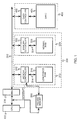
- the virtual address space of a central processing unit (CPU) 100 is mapped into the physical address space of a system RAM 300 via the page table function of a memory management unit (MMU) 200 and the page swapping function of the operating system's memory manager.
- System RAM 300 is a fast, volatile RAM memory and provides the working storage used by CPU 100.
- Mass storage 400 may also be available to MMU 200.
- Mass storage 400 includes a direct access storage device (DASD) 404 and a corresponding DASD controller 402.
- DASD 404 may be represented by a magnetic or an optical disk.
- System RAM 300 is divided into two memory banks: a low-power memory bank 310 and a normal memory bank 320.
- Low-power memory bank 310 includes a memory controller 312 and a low-power RAM 316.
- Normal memory bank 320 includes a memory controller 322 and a normal RAM 326.
- RAM microcircuit chips of memories 316 and 326 are available in convenient packages known as Single In-Line Memory Modules or SIMM.
- SIMM's are the preferred embodiment of memories 316 and 326.
- Memory controllers 312 and 322 each contain both driver circuits and logic circuits.
- the driver circuits perform the reading from, and writing to, the RAM memory.
- the logic circuits are responsible for detecting an address reference to, and generating control signals and address data for, each corresponding physical memory location.
- a memory 500 Each read from or write to a page of memory is called a memory "reference”.
- the number of references per unit time is the "reference frequency”.
- a private memory 500 is provided for storing memory reference information.
- Every page of virtual memory may be represented by a page in system RAM 300 and/or, if a page hasn't been referenced for a relatively long period of time, in mass storage 400.
- the page table or memory map is maintained by the memory manager and keeps track of where each virtual page is physically represented.
- This invention is primarily concerned with reducing the power consumption of system RAM 300 by controlling the placement of the physical pages. The placement is done according to the reference frequency for each particular virtual page.
- Normal RAM 326 of normal memory 320 is a high speed, high power RAM memory.
- the less frequently used pages of memory are stored in low-power memory 310.
- Low-power RAM 316 will consume less power and will therefore tend to be slower than normal RAM 326.
- This optimization scheme balances the performance cost of migrating a page between the two memory banks with the higher power cost associated with leaving the page in normal memory 320. Power savings are achieved because low-power RAM 316 tends to consume less power than the faster high-power RAM which is conventionally used throughout system RAM 300.
- driver circuits of memory controller 312 drive both system bus 202 and corresponding SIMM buses 314 and 324, respectively. These driver circuits are responsible for the majority of the power consumed by memory banks 310 and 320. Under normal conditions, the refresh cycle of the RAM and the logic circuits use only a nominal amount of power.
- the driver circuits of memory controller 312 are powered independent of the logic circuits and are operable in two states: a first active state and a second standby or sleep state.
- the driver circuits function normally and may satisfy a memory reference.
- the sleep state however, power is removed from the driver circuits so that they are passive rather than active circuit elements.
- the memory controller is not capable of satisfying a memory reference.
- the memory controller logic circuits will decode the physical address received from the MMU and reference the actual memory cells through the driver circuits. If the driver circuits of memory controller 312 are in the sleep state when the CPU makes a reference to a page in low-power memory 310, then the memory controller 312 will be unable to satisfy the request because the driver circuits are inactive. Thus, the logic circuits must be able to sense that a reference has been made and apply power to the driver circuits.
- Determination of whether a page belongs in normal memory 320 or in low-power memory 310 is the function of a page placement daemon.
- the daemon is part of the operating system's memory manager.
- the daemon is loaded as a background process during system initialization and thereafter remains inactive until invoked by an interrupt.
- the daemon Upon receiving an interrupt, the daemon calculates the reference frequency for each page in low-power memory 310 and then makes a decision based on set criteria on whether to migrate each page to normal memory 320.
- the daemon In order to make the determination of proper location for a page of memory, the daemon must have access to reference information for each page of memory in low-power memory 310.
- the preferred way for maintaining a reference count utilizes private memory 500.
- Private memory 500 is organized as a table for storing page addresses.
- the daemon does not write to this memory, but may read it and may reset the table pointer.
- the page address of the particular page is written to private memory 500 by memory controller 312 at a location indicated by the table pointer for the private memory. For example, given a 4 kB page size with 32 bit addressing, the private memory would be a 100 kB memory organized as a table 20 bits wide. The top (or most significant) 20 bits of the address identify the particular page and would be written into the table by memory controller 312 as the next table entry and the table pointer would be incremented.
- memory controller 312 produces a specific interrupt to processor 100. This interrupt invokes the daemon. With reference to Figure 3, the daemon then performs the following steps:
- a page will have to be swapped out to make room for the incoming page.
- the page to be swapped out may be selected by any number of ad hoc rules or as a function of its frequency of reference.
- the preferred means for making the transfer is the page swapper of the resident operating system. All page-oriented operating systems have a page swapper, which is part of the memory manager.
- the page swapper When the page swapper moves a page from low-power memory 310 to normal memory 320, it will normally have to bump a page out of normal memory 320 and into low-power memory 310. As discussed above, it will need to choose which page to move out of normal memory 320. If a means involving a private memory and the daemon is not employed to classify pages of normal memory 320 according to their frequency of reference, then the preferred method is for the page swapper to use the same steps which it employs in deciding when to move a page from system RAM 300 to mass storage.
- the daemon may keep track of references to low-power memory 310 directly in the operating system's page table. In this embodiment, upon sensing a reference to a page of low-power RAM 316, memory controller 312 would produce an interrupt to the daemon.
- the daemon Upon receiving an interrupt, the daemon will make a decision based on set criteria on how to handle the memory reference. It has two options: first, if the daemon determines that the page is not referenced with sufficient frequency to justify moving that page to normal memory 320, then the daemon will simply turn on the driver circuits so that the reference can be made and then set a timer which will turn the driver circuits back off after a fixed period; second, if the daemon determines that the page is referenced with sufficient frequency, then the daemon will turn on the driver circuits, set a timer which will turn the driver circuits back off after a fixed period, and either call the operating system's page swapper which will transfer the page of memory to normal memory 320, or the daemon may make the transfer itself.
- This alternate embodiment involves numerous additional instructions and will result in an increased overhead burden on CPU 100 relative to the first embodiment.
Applications Claiming Priority (2)
| Application Number | Priority Date | Filing Date | Title |
|---|---|---|---|
| US60483890A | 1990-10-29 | 1990-10-29 | |
| US604838 | 1990-10-29 |
Publications (3)
| Publication Number | Publication Date |
|---|---|
| EP0483525A2 true EP0483525A2 (fr) | 1992-05-06 |
| EP0483525A3 EP0483525A3 (en) | 1993-02-24 |
| EP0483525B1 EP0483525B1 (fr) | 1997-03-19 |
Family
ID=24421253
Family Applications (1)
| Application Number | Title | Priority Date | Filing Date |
|---|---|---|---|
| EP91116616A Expired - Lifetime EP0483525B1 (fr) | 1990-10-29 | 1991-09-28 | Gestion de tension d'alimentation pour station de travail |
Country Status (4)
| Country | Link |
|---|---|
| US (1) | US5390334A (fr) |
| EP (1) | EP0483525B1 (fr) |
| JP (1) | JPH04230508A (fr) |
| DE (1) | DE69125242D1 (fr) |
Cited By (5)
| Publication number | Priority date | Publication date | Assignee | Title |
|---|---|---|---|---|
| WO2001095106A2 (fr) * | 2000-06-02 | 2001-12-13 | Sun Microsystems, Inc. | Tas virtuel destine a une machine virtuelle |
| US6934755B1 (en) | 2000-06-02 | 2005-08-23 | Sun Microsystems, Inc. | System and method for migrating processes on a network |
| DE102009037235A1 (de) | 2008-10-14 | 2010-04-15 | Giesecke & Devrient Gmbh | Speicherverwaltung in einem portablem Datenträger |
| WO2011139465A2 (fr) | 2010-04-30 | 2011-11-10 | Microsoft Corporation | Examen de l'utilisation de la mémoire |
| US10620879B2 (en) * | 2017-05-17 | 2020-04-14 | Macronix International Co., Ltd. | Write-while-read access method for a memory device |
Families Citing this family (69)
| Publication number | Priority date | Publication date | Assignee | Title |
|---|---|---|---|---|
| JP3058986B2 (ja) * | 1992-04-02 | 2000-07-04 | ダイヤセミコンシステムズ株式会社 | コンピュータシステムの節電制御装置 |
| US5524248A (en) * | 1993-07-06 | 1996-06-04 | Dell Usa, L.P. | Random access memory power management system |
| KR100352045B1 (ko) * | 1994-01-10 | 2002-12-28 | 선 마이크로시스템즈 인코퍼레이티드 | 컴퓨터시스템에서전력소모를감소시키기위한방법및장치 |
| DE69516199T2 (de) * | 1994-02-23 | 2000-09-21 | Sun Microsystems Inc | Verfahren und Anordnung zur Leistungseinsparung in einem Computersystem unter Benutzung eines Leistungssteuerungs-Pseudogeräte-Treibers |
| US5778443A (en) * | 1994-12-14 | 1998-07-07 | International Business Machines Corp. | Method and apparatus for conserving power and system resources in a computer system employing a virtual memory |
| US5710933A (en) * | 1995-03-31 | 1998-01-20 | International Business Machines Corporation | System resource enable apparatus |
| US6408393B1 (en) * | 1998-01-09 | 2002-06-18 | Hitachi, Ltd. | CPU power adjustment method |
| JP2000215100A (ja) * | 1999-01-21 | 2000-08-04 | Nec Corp | 省電力メモリ管理システム |
| US6516381B1 (en) * | 1999-09-28 | 2003-02-04 | Intel Corporation | Supplying voltage to a memory module |
| US6957237B1 (en) | 2000-06-02 | 2005-10-18 | Sun Microsystems, Inc. | Database store for a virtual heap |
| US6854115B1 (en) | 2000-06-02 | 2005-02-08 | Sun Microsystems, Inc. | Process persistence in a virtual machine |
| JP2002268778A (ja) * | 2001-03-14 | 2002-09-20 | Toshiba Corp | 情報処理装置 |
| US6820169B2 (en) * | 2001-09-25 | 2004-11-16 | Intel Corporation | Memory control with lookahead power management |
| US6766420B2 (en) * | 2001-09-27 | 2004-07-20 | International Business Machines Corporation | Selectively powering portions of system memory in a network server to conserve energy |
| US7330954B2 (en) * | 2002-04-18 | 2008-02-12 | Intel Corporation | Storing information in one of at least two storage devices based on a storage parameter and an attribute of the storage devices |
| US7721292B2 (en) * | 2004-12-16 | 2010-05-18 | International Business Machines Corporation | System for adjusting resource allocation to a logical partition based on rate of page swaps and utilization by changing a boot configuration file |
| GB2426360A (en) * | 2005-05-18 | 2006-11-22 | Symbian Software Ltd | Reorganisation of memory for conserving power in a computing device |
| US8796830B1 (en) | 2006-09-01 | 2014-08-05 | Google Inc. | Stackable low-profile lead frame package |
| US8327104B2 (en) * | 2006-07-31 | 2012-12-04 | Google Inc. | Adjusting the timing of signals associated with a memory system |
| US8397013B1 (en) | 2006-10-05 | 2013-03-12 | Google Inc. | Hybrid memory module |
| US8055833B2 (en) | 2006-10-05 | 2011-11-08 | Google Inc. | System and method for increasing capacity, performance, and flexibility of flash storage |
| US8111566B1 (en) | 2007-11-16 | 2012-02-07 | Google, Inc. | Optimal channel design for memory devices for providing a high-speed memory interface |
| US8244971B2 (en) * | 2006-07-31 | 2012-08-14 | Google Inc. | Memory circuit system and method |
| US8077535B2 (en) * | 2006-07-31 | 2011-12-13 | Google Inc. | Memory refresh apparatus and method |
| US8335894B1 (en) | 2008-07-25 | 2012-12-18 | Google Inc. | Configurable memory system with interface circuit |
| US8619452B2 (en) | 2005-09-02 | 2013-12-31 | Google Inc. | Methods and apparatus of stacking DRAMs |
| KR101318116B1 (ko) * | 2005-06-24 | 2013-11-14 | 구글 인코포레이티드 | 집적 메모리 코어 및 메모리 인터페이스 회로 |
| US8041881B2 (en) | 2006-07-31 | 2011-10-18 | Google Inc. | Memory device with emulated characteristics |
| US20080028136A1 (en) * | 2006-07-31 | 2008-01-31 | Schakel Keith R | Method and apparatus for refresh management of memory modules |
| US9507739B2 (en) | 2005-06-24 | 2016-11-29 | Google Inc. | Configurable memory circuit system and method |
| US8090897B2 (en) | 2006-07-31 | 2012-01-03 | Google Inc. | System and method for simulating an aspect of a memory circuit |
| US20080126690A1 (en) * | 2006-02-09 | 2008-05-29 | Rajan Suresh N | Memory module with memory stack |
| US9542352B2 (en) * | 2006-02-09 | 2017-01-10 | Google Inc. | System and method for reducing command scheduling constraints of memory circuits |
| US9171585B2 (en) | 2005-06-24 | 2015-10-27 | Google Inc. | Configurable memory circuit system and method |
| US7609567B2 (en) * | 2005-06-24 | 2009-10-27 | Metaram, Inc. | System and method for simulating an aspect of a memory circuit |
| US10013371B2 (en) | 2005-06-24 | 2018-07-03 | Google Llc | Configurable memory circuit system and method |
| US7386656B2 (en) | 2006-07-31 | 2008-06-10 | Metaram, Inc. | Interface circuit system and method for performing power management operations in conjunction with only a portion of a memory circuit |
| US20080082763A1 (en) | 2006-10-02 | 2008-04-03 | Metaram, Inc. | Apparatus and method for power management of memory circuits by a system or component thereof |
| US8438328B2 (en) | 2008-02-21 | 2013-05-07 | Google Inc. | Emulation of abstracted DIMMs using abstracted DRAMs |
| US8359187B2 (en) * | 2005-06-24 | 2013-01-22 | Google Inc. | Simulating a different number of memory circuit devices |
| US8386722B1 (en) | 2008-06-23 | 2013-02-26 | Google Inc. | Stacked DIMM memory interface |
| US8081474B1 (en) | 2007-12-18 | 2011-12-20 | Google Inc. | Embossed heat spreader |
| US8089795B2 (en) | 2006-02-09 | 2012-01-03 | Google Inc. | Memory module with memory stack and interface with enhanced capabilities |
| US8060774B2 (en) | 2005-06-24 | 2011-11-15 | Google Inc. | Memory systems and memory modules |
| US8130560B1 (en) | 2006-11-13 | 2012-03-06 | Google Inc. | Multi-rank partial width memory modules |
| US7543123B2 (en) * | 2005-11-07 | 2009-06-02 | International Business Machines Corporation | Multistage virtual memory paging system |
| US20070124522A1 (en) * | 2005-11-30 | 2007-05-31 | Ellison Brandon J | Node detach in multi-node system |
| US9632929B2 (en) | 2006-02-09 | 2017-04-25 | Google Inc. | Translating an address associated with a command communicated between a system and memory circuits |
| US7724589B2 (en) * | 2006-07-31 | 2010-05-25 | Google Inc. | System and method for delaying a signal communicated from a system to at least one of a plurality of memory circuits |
| US20080028137A1 (en) * | 2006-07-31 | 2008-01-31 | Schakel Keith R | Method and Apparatus For Refresh Management of Memory Modules |
| US20080025136A1 (en) * | 2006-07-31 | 2008-01-31 | Metaram, Inc. | System and method for storing at least a portion of information received in association with a first operation for use in performing a second operation |
| US7873801B2 (en) * | 2007-02-01 | 2011-01-18 | Oracle America, Inc. | Partitionable accounting of memory utilization |
| US20080229050A1 (en) * | 2007-03-13 | 2008-09-18 | Sony Ericsson Mobile Communications Ab | Dynamic page on demand buffer size for power savings |
| US8209479B2 (en) * | 2007-07-18 | 2012-06-26 | Google Inc. | Memory circuit system and method |
| US8080874B1 (en) | 2007-09-14 | 2011-12-20 | Google Inc. | Providing additional space between an integrated circuit and a circuit board for positioning a component therebetween |
| JP4958723B2 (ja) * | 2007-10-19 | 2012-06-20 | 株式会社リコー | 仮想記憶制御装置、仮想記憶制御方法、仮想記憶制御プログラム及び記録媒体 |
| JP4902501B2 (ja) * | 2007-11-12 | 2012-03-21 | 株式会社日立製作所 | 電力制御方法、計算機システム、及びプログラム |
| EP2441007A1 (fr) * | 2009-06-09 | 2012-04-18 | Google, Inc. | Programmation de valeurs de résistance de terminaison dimm |
| US8799553B2 (en) * | 2010-04-13 | 2014-08-05 | Apple Inc. | Memory controller mapping on-the-fly |
| US8484418B2 (en) * | 2010-10-22 | 2013-07-09 | Intel Corporation | Methods and apparatuses for idle-prioritized memory ranks |
| US9235500B2 (en) | 2010-12-07 | 2016-01-12 | Microsoft Technology Licensing, Llc | Dynamic memory allocation and relocation to create low power regions |
| JP5775398B2 (ja) * | 2011-08-25 | 2015-09-09 | ルネサスエレクトロニクス株式会社 | 半導体集積回路装置 |
| US9047090B2 (en) * | 2012-08-07 | 2015-06-02 | Qualcomm Incorporated | Methods, systems and devices for hybrid memory management |
| US11099789B2 (en) | 2018-02-05 | 2021-08-24 | Micron Technology, Inc. | Remote direct memory access in multi-tier memory systems |
| US10782908B2 (en) | 2018-02-05 | 2020-09-22 | Micron Technology, Inc. | Predictive data orchestration in multi-tier memory systems |
| US11416395B2 (en) * | 2018-02-05 | 2022-08-16 | Micron Technology, Inc. | Memory virtualization for accessing heterogeneous memory components |
| US10880401B2 (en) | 2018-02-12 | 2020-12-29 | Micron Technology, Inc. | Optimization of data access and communication in memory systems |
| US10877892B2 (en) | 2018-07-11 | 2020-12-29 | Micron Technology, Inc. | Predictive paging to accelerate memory access |
| US10852949B2 (en) | 2019-04-15 | 2020-12-01 | Micron Technology, Inc. | Predictive data pre-fetching in a data storage device |
Citations (1)
| Publication number | Priority date | Publication date | Assignee | Title |
|---|---|---|---|---|
| US3703710A (en) * | 1970-01-05 | 1972-11-21 | Hitachi Ltd | Semiconductor memory |
Family Cites Families (25)
| Publication number | Priority date | Publication date | Assignee | Title |
|---|---|---|---|---|
| US3701107A (en) * | 1970-10-01 | 1972-10-24 | Rca Corp | Computer with probability means to transfer pages from large memory to fast memory |
| GB1504112A (en) * | 1976-03-17 | 1978-03-15 | Ibm | Interactive enquiry systems |
| JPS54136237A (en) * | 1978-04-14 | 1979-10-23 | Fujitsu Ltd | Memory unit access system |
| US4277826A (en) * | 1978-10-23 | 1981-07-07 | Collins Robert W | Synchronizing mechanism for page replacement control |
| US4868734A (en) * | 1984-04-30 | 1989-09-19 | Unisys Corp. | Variable rate improvement of disc cache subsystem |
| JPS5635228A (en) * | 1979-08-31 | 1981-04-07 | Fujitsu Ltd | Power supply system for memory device |
| US4463424A (en) * | 1981-02-19 | 1984-07-31 | International Business Machines Corporation | Method for dynamically allocating LRU/MRU managed memory among concurrent sequential processes |
| US4475194A (en) * | 1982-03-30 | 1984-10-02 | International Business Machines Corporation | Dynamic replacement of defective memory words |
| US4736287A (en) * | 1983-06-20 | 1988-04-05 | Rational | Set association memory system |
| US4737867A (en) * | 1984-02-03 | 1988-04-12 | Brother Kogyo Kabushiki Kaisha | Power saving arrangement in information recording system |
| JPS60177466A (ja) * | 1984-02-22 | 1985-09-11 | Sharp Corp | フロツピ−・デイスク・ドライブ制御方式 |
| US4680703A (en) * | 1984-06-25 | 1987-07-14 | International Business Machines Corp. | Data processing system with reorganization of disk storage for improved paging |
| US4660130A (en) * | 1984-07-24 | 1987-04-21 | Texas Instruments Incorporated | Method for managing virtual memory to separate active and stable memory blocks |
| US4758944A (en) * | 1984-08-24 | 1988-07-19 | Texas Instruments Incorporated | Method for managing virtual memory to separate active and stable memory blocks |
| US4653050A (en) * | 1984-12-03 | 1987-03-24 | Trw Inc. | Fault-tolerant memory system |
| JPS63201828A (ja) * | 1987-02-18 | 1988-08-19 | Hitachi Ltd | 情報処理装置 |
| JPS6451512A (en) * | 1987-08-22 | 1989-02-27 | Fuji Photo Film Co Ltd | Power saving type memory device |
| US5157774A (en) * | 1987-09-28 | 1992-10-20 | Compaq Computer Corporation | System for fast selection of non-cacheable address ranges using programmed array logic |
| US5091850A (en) * | 1987-09-28 | 1992-02-25 | Compaq Computer Corporation | System for fast selection of non-cacheable address ranges using programmed array logic |
| JPS6488661A (en) * | 1987-09-29 | 1989-04-03 | Toshiba Corp | Virtual memory control and management system |
| US5226147A (en) * | 1987-11-06 | 1993-07-06 | Mitsubishi Denki Kabushiki Kaisha | Semiconductor memory device for simple cache system |
| JPH02273843A (ja) * | 1989-04-14 | 1990-11-08 | Nec Corp | スワッピング装置 |
| US5218686A (en) * | 1989-11-03 | 1993-06-08 | Compaq Computer Corporation | Combined synchronous and asynchronous memory controller |
| JP2938511B2 (ja) * | 1990-03-30 | 1999-08-23 | 三菱電機株式会社 | 半導体記憶装置 |
| US5249282A (en) * | 1990-11-21 | 1993-09-28 | Benchmarq Microelectronics, Inc. | Integrated cache memory system with primary and secondary cache memories |
-
1991
- 1991-07-18 JP JP3202230A patent/JPH04230508A/ja active Pending
- 1991-09-28 EP EP91116616A patent/EP0483525B1/fr not_active Expired - Lifetime
- 1991-09-28 DE DE69125242T patent/DE69125242D1/de not_active Expired - Lifetime
-
1992
- 1992-11-09 US US07/973,574 patent/US5390334A/en not_active Expired - Fee Related
Patent Citations (1)
| Publication number | Priority date | Publication date | Assignee | Title |
|---|---|---|---|---|
| US3703710A (en) * | 1970-01-05 | 1972-11-21 | Hitachi Ltd | Semiconductor memory |
Non-Patent Citations (4)
| Title |
|---|
| COMPUTER DESIGN vol. 11, no. 1, January 1972, LITTLETON, MASSACHUSETTS US pages 45 - 49 JOHN G WILLIAMS 'Large-core Storage in Perspective' * |
| ELECTRONICS LETTERS vol. 14, no. 16, 3 August 1978, STEVENAGE GB pages 498 - 499 D J WHEELER 'Computer store enhancement by interchange' * |
| IBM TECHNICAL DISCLOSURE BULLETIN. vol. 22, no. 3, August 1979, NEW YORK US pages 1057 - 1058 BLUM ET AL 'Fast multichip memorysystem with power select signal' * |
| SIEWIOREK, BELL AND NEWELL 'Computer Structures: Principles and Examples' 1982 , MC GRAW-HILL , TOKYO, JP * |
Cited By (10)
| Publication number | Priority date | Publication date | Assignee | Title |
|---|---|---|---|---|
| WO2001095106A2 (fr) * | 2000-06-02 | 2001-12-13 | Sun Microsystems, Inc. | Tas virtuel destine a une machine virtuelle |
| WO2001095106A3 (fr) * | 2000-06-02 | 2003-01-30 | Sun Microsystems Inc | Tas virtuel destine a une machine virtuelle |
| US6934755B1 (en) | 2000-06-02 | 2005-08-23 | Sun Microsystems, Inc. | System and method for migrating processes on a network |
| DE102009037235A1 (de) | 2008-10-14 | 2010-04-15 | Giesecke & Devrient Gmbh | Speicherverwaltung in einem portablem Datenträger |
| EP2177990A1 (fr) | 2008-10-14 | 2010-04-21 | Giesecke & Devrient GmbH | Gestion de mémoire dans un support de données portable |
| WO2011139465A2 (fr) | 2010-04-30 | 2011-11-10 | Microsoft Corporation | Examen de l'utilisation de la mémoire |
| EP2564321A2 (fr) * | 2010-04-30 | 2013-03-06 | Microsoft Corporation | Examen de l'utilisation de la mémoire |
| EP2564321A4 (fr) * | 2010-04-30 | 2015-01-14 | Microsoft Corp | Examen de l'utilisation de la mémoire |
| US9015441B2 (en) | 2010-04-30 | 2015-04-21 | Microsoft Technology Licensing, Llc | Memory usage scanning |
| US10620879B2 (en) * | 2017-05-17 | 2020-04-14 | Macronix International Co., Ltd. | Write-while-read access method for a memory device |
Also Published As
| Publication number | Publication date |
|---|---|
| EP0483525A3 (en) | 1993-02-24 |
| DE69125242D1 (de) | 1997-04-24 |
| EP0483525B1 (fr) | 1997-03-19 |
| US5390334A (en) | 1995-02-14 |
| JPH04230508A (ja) | 1992-08-19 |
Similar Documents
| Publication | Publication Date | Title |
|---|---|---|
| US5390334A (en) | Workstation power management by page placement control | |
| US6546472B2 (en) | Fast suspend to disk | |
| US7640443B2 (en) | Computer apparatus, storage apparatus, system management apparatus, and hard disk unit power supply controlling method | |
| CN100487632C (zh) | 双媒体存储装置 | |
| US6732241B2 (en) | Technique for migrating data between storage devices for reduced power consumption | |
| US5632038A (en) | Secondary cache system for portable computer | |
| EP1127308B1 (fr) | Procede et appareil destines a la gestion de la consommation d'energie dans un sous-systeme de memoire | |
| US5584012A (en) | Cache control method and rotary storage device having cache control | |
| US5826092A (en) | Method and apparatus for performance optimization in power-managed computer systems | |
| JPH07219848A (ja) | キャッシュ制御システム | |
| US20080005461A1 (en) | Power-saving control apparatus, power-saving control method, and computer product | |
| CN102495756A (zh) | 操作系统在不同的中央处理器之间切换的方法及系统 | |
| US20030079087A1 (en) | Cache memory control unit and method | |
| US20120284475A1 (en) | Memory On-Demand, Managing Power In Memory | |
| WO2005069148A2 (fr) | Procede de gestion de memoire et systeme associe | |
| US20050185496A1 (en) | Intelligent solid state disk | |
| CN101520689A (zh) | 一种计算机存储设备控制方法、控制器及存储设备 | |
| JP2002297320A (ja) | ディスクアレイ装置 | |
| CN1177279C (zh) | 维持动态随机存取存储器的存储数据的方法及相关装置 | |
| JP3541349B2 (ja) | キャッシュメモリ・バックアップシステム | |
| US7543127B2 (en) | Computer system | |
| JPS60179857A (ja) | キヤツシユ装置の制御方式 | |
| JP3961669B2 (ja) | コンピュータシステムおよびデータ転送制御方法 | |
| CN1268686A (zh) | 使用闪存作开机环境设定的软硬件配置 | |
| CN115202466A (zh) | 闪存控制器及电源管理方法 |
Legal Events
| Date | Code | Title | Description |
|---|---|---|---|
| PUAI | Public reference made under article 153(3) epc to a published international application that has entered the european phase |
Free format text: ORIGINAL CODE: 0009012 |
|
| AK | Designated contracting states |
Kind code of ref document: A2 Designated state(s): DE FR GB |
|
| 17P | Request for examination filed |
Effective date: 19920817 |
|
| PUAL | Search report despatched |
Free format text: ORIGINAL CODE: 0009013 |
|
| AK | Designated contracting states |
Kind code of ref document: A3 Designated state(s): DE FR GB |
|
| 17Q | First examination report despatched |
Effective date: 19951011 |
|
| GRAG | Despatch of communication of intention to grant |
Free format text: ORIGINAL CODE: EPIDOS AGRA |
|
| GRAH | Despatch of communication of intention to grant a patent |
Free format text: ORIGINAL CODE: EPIDOS IGRA |
|
| GRAH | Despatch of communication of intention to grant a patent |
Free format text: ORIGINAL CODE: EPIDOS IGRA |
|
| GRAH | Despatch of communication of intention to grant a patent |
Free format text: ORIGINAL CODE: EPIDOS IGRA |
|
| GRAA | (expected) grant |
Free format text: ORIGINAL CODE: 0009210 |
|
| AK | Designated contracting states |
Kind code of ref document: B1 Designated state(s): DE FR GB |
|
| PG25 | Lapsed in a contracting state [announced via postgrant information from national office to epo] |
Ref country code: FR Effective date: 19970319 |
|
| REF | Corresponds to: |
Ref document number: 69125242 Country of ref document: DE Date of ref document: 19970424 |
|
| PG25 | Lapsed in a contracting state [announced via postgrant information from national office to epo] |
Ref country code: DE Effective date: 19970620 |
|
| EN | Fr: translation not filed | ||
| PG25 | Lapsed in a contracting state [announced via postgrant information from national office to epo] |
Ref country code: GB Free format text: LAPSE BECAUSE OF NON-PAYMENT OF DUE FEES Effective date: 19970928 |
|
| PLBE | No opposition filed within time limit |
Free format text: ORIGINAL CODE: 0009261 |
|
| STAA | Information on the status of an ep patent application or granted ep patent |
Free format text: STATUS: NO OPPOSITION FILED WITHIN TIME LIMIT |
|
| 26N | No opposition filed | ||
| GBPC | Gb: european patent ceased through non-payment of renewal fee |
Effective date: 19970928 |