EP0481016B1 - Erlöschungsschaltung für lawinenfotodioden - Google Patents
Erlöschungsschaltung für lawinenfotodioden Download PDFInfo
- Publication number
- EP0481016B1 EP0481016B1 EP90917799A EP90917799A EP0481016B1 EP 0481016 B1 EP0481016 B1 EP 0481016B1 EP 90917799 A EP90917799 A EP 90917799A EP 90917799 A EP90917799 A EP 90917799A EP 0481016 B1 EP0481016 B1 EP 0481016B1
- Authority
- EP
- European Patent Office
- Prior art keywords
- circuit
- comparator
- avalanche
- photodiode
- voltage
- Prior art date
- Legal status (The legal status is an assumption and is not a legal conclusion. Google has not performed a legal analysis and makes no representation as to the accuracy of the status listed.)
- Expired - Lifetime
Links
- 238000010791 quenching Methods 0.000 title claims abstract description 56
- 230000000171 quenching effect Effects 0.000 title claims abstract description 29
- 230000004044 response Effects 0.000 claims abstract description 19
- 230000000977 initiatory effect Effects 0.000 claims abstract description 13
- 230000009467 reduction Effects 0.000 claims abstract description 7
- 230000008859 change Effects 0.000 claims description 17
- 238000001514 detection method Methods 0.000 claims description 17
- 230000003213 activating effect Effects 0.000 claims description 2
- 230000004913 activation Effects 0.000 claims description 2
- 238000005259 measurement Methods 0.000 description 10
- 238000010521 absorption reaction Methods 0.000 description 9
- 230000015556 catabolic process Effects 0.000 description 8
- 230000000875 corresponding effect Effects 0.000 description 6
- 230000000694 effects Effects 0.000 description 4
- 238000004599 local-density approximation Methods 0.000 description 3
- 230000007704 transition Effects 0.000 description 3
- 238000013459 approach Methods 0.000 description 2
- 230000008901 benefit Effects 0.000 description 2
- 239000003990 capacitor Substances 0.000 description 2
- 238000012937 correction Methods 0.000 description 2
- 239000012530 fluid Substances 0.000 description 2
- 238000004519 manufacturing process Methods 0.000 description 2
- 238000000034 method Methods 0.000 description 2
- 230000004048 modification Effects 0.000 description 2
- 238000012986 modification Methods 0.000 description 2
- 239000002245 particle Substances 0.000 description 2
- 239000004065 semiconductor Substances 0.000 description 2
- 230000035945 sensitivity Effects 0.000 description 2
- 230000001960 triggered effect Effects 0.000 description 2
- 238000004458 analytical method Methods 0.000 description 1
- 238000005311 autocorrelation function Methods 0.000 description 1
- 230000004888 barrier function Effects 0.000 description 1
- 239000002800 charge carrier Substances 0.000 description 1
- 230000002596 correlated effect Effects 0.000 description 1
- 238000005314 correlation function Methods 0.000 description 1
- 230000008878 coupling Effects 0.000 description 1
- 238000010168 coupling process Methods 0.000 description 1
- 238000005859 coupling reaction Methods 0.000 description 1
- 230000007547 defect Effects 0.000 description 1
- 238000002296 dynamic light scattering Methods 0.000 description 1
- 238000002474 experimental method Methods 0.000 description 1
- 238000000752 ionisation method Methods 0.000 description 1
- 238000001307 laser spectroscopy Methods 0.000 description 1
- 239000000463 material Substances 0.000 description 1
- 238000012544 monitoring process Methods 0.000 description 1
- 230000000704 physical effect Effects 0.000 description 1
- 238000011084 recovery Methods 0.000 description 1
- 230000002459 sustained effect Effects 0.000 description 1
- 230000001052 transient effect Effects 0.000 description 1
Images


Classifications
-
- G—PHYSICS
- G01—MEASURING; TESTING
- G01J—MEASUREMENT OF INTENSITY, VELOCITY, SPECTRAL CONTENT, POLARISATION, PHASE OR PULSE CHARACTERISTICS OF INFRARED, VISIBLE OR ULTRAVIOLET LIGHT; COLORIMETRY; RADIATION PYROMETRY
- G01J1/00—Photometry, e.g. photographic exposure meter
- G01J1/42—Photometry, e.g. photographic exposure meter using electric radiation detectors
- G01J1/44—Electric circuits
-
- G—PHYSICS
- G01—MEASURING; TESTING
- G01S—RADIO DIRECTION-FINDING; RADIO NAVIGATION; DETERMINING DISTANCE OR VELOCITY BY USE OF RADIO WAVES; LOCATING OR PRESENCE-DETECTING BY USE OF THE REFLECTION OR RERADIATION OF RADIO WAVES; ANALOGOUS ARRANGEMENTS USING OTHER WAVES
- G01S7/00—Details of systems according to groups G01S13/00, G01S15/00, G01S17/00
- G01S7/48—Details of systems according to groups G01S13/00, G01S15/00, G01S17/00 of systems according to group G01S17/00
- G01S7/483—Details of pulse systems
- G01S7/486—Receivers
- G01S7/4861—Circuits for detection, sampling, integration or read-out
-
- G—PHYSICS
- G01—MEASURING; TESTING
- G01J—MEASUREMENT OF INTENSITY, VELOCITY, SPECTRAL CONTENT, POLARISATION, PHASE OR PULSE CHARACTERISTICS OF INFRARED, VISIBLE OR ULTRAVIOLET LIGHT; COLORIMETRY; RADIATION PYROMETRY
- G01J1/00—Photometry, e.g. photographic exposure meter
- G01J1/42—Photometry, e.g. photographic exposure meter using electric radiation detectors
- G01J1/44—Electric circuits
- G01J2001/4446—Type of detector
- G01J2001/446—Photodiode
- G01J2001/4466—Avalanche
Definitions
- This invention relates to an avalanche photodiode quenching circuit for use in photon counting measurements.
- Photon counting measurements were originally, and are to some extent presently, carried out using photomultiplier tubes for photon detection.
- a typical photomultiplier is however relatively fragile, bulky and expensive.
- the search for a more convenient alternative has led to the use of photodiodes operated in the so-called avalanche Geiger mode. This mode entails reverse-biasing the photodiode with a bias voltage typically a few volts greater than the photodiode breakdown voltage V BR .
- V BR is the voltage at which a single photon absorption produces complete electrical breakdown of the photodiode active region by cascaded collision ionisation. It is analogous to the ionisation processes occurring in the gas phase in a Geiger-Muller tube.
- Avalanche photodiodes are comparatively inexpensive and rugged, and exhibit high quantum efficiencies. They are not however without disadvantages. In particular, for the purposes of achieving high quantum efficiencies, it is necessary to operate at reverse voltages at least bordering on that capable of producing a self-sustaining avalanche in the photodiode. If the photodiode avalanche current reaches a value referred to as I latch , typically 50 microamps, the avalanche is self-sustaining in the absence of further photons. This may produce catastrophic failure. The photodiode is substantially insensitive to photons while in the avalanche condition.
- passive quenching involves arranging the photodiode in series with a comparatively large series resistor, eg 220 Kohm, and applying the bias voltage across the series arrangement. Prior to photon absorption, ie when the photodiode is quiescent, the bias appears across the substantially non-conducting photodiode. After absorption, the resistor limits the maximum current taken by the photodiode to a value below I latch when the falling voltage across the photodiode becomes equal to V BR . The avalanche is therefore automatically terminated.
- Dead-time limitations render the passively quenched avalanche photodiode suitable for photon correlation laser anemometry and spectroscopy experiments where the photon correlator sample time or delay is greater than a few microseconds.
- light intensity fluctuation frequencies greater than 1 MHz regularly occur in photon correlation measurements on particle diameters of a few tens of nanometres, and also in transonic and supersonic fluid flow measurements by laser Doppler anemometry.
- a passively quenched avalanche photodiode is not capable of detecting such frequencies.
- the photodiode has a reverse voltage of about 4 V in excess of its breakdown voltage V BR , and it is required to detect an avalanche as soon as possible after this voltage has begun to fall. It is necessary for the quenching circuit to respond to a fall of a few tens of millivolts. Moreover, the reset pulse is required to re-establish the original photodiode reverse voltage very accurately without re-triggering the feedback circuit and generating a spurious count. In practice this is difficult to achieve. Furthermore, the circuits are characterised by an ill-defined dead-time. Photon absorption events which are too close together in time produce a situation in which a counter has not fully recovered from a first pulse before it receives a second, and the second is not detected.
- a further quenching circuit for an avalanche photodiode is described in International Application No WO 88/04034 published under the Patent Co-operation Treaty on 2 June 1988. It provides for active quenching of a photodiode current avalanche, but the photodiode is subsequently isolated to allow recharge through a low value ballast resistor. This combines active quenching with passive reset, the reset operation being rapid by virtue of the low value (1 Kohm) of the ballast resistor. Initiation of an avalanche is sensed by a comparator, which responds rapidly by reducing the photodiode voltage below breakdown via a quench circuit. This also isolates the photodiode from the comparator.
- the comparator input is then reset to its original level, and the consequent change in comparator output terminates the quench operation allowing the photodiode to recharge.
- the change in comparator output also terminates the reset operation, by which time the photodiode has recharged.
- the recharge rate is much more rapid than in earlier passive quench-passive reset arrangements.
- This circuit provides an accurately defined dead-time in the region of 50 nanoseconds, substantially constant output pulse width, reliable quenching and high speed operation. In principle it can operate at photon counting rates up to 20 MHz, and provides good protection against after pulsing and the odd-even effect previously referred to.
- the present invention provides an avalanche photodiode quenching circuit including an avalanche photodiode rechargeable through a ballast resistor, an avalanche detection amplifier having an input connected to receive a signal from the photodiode and arranged to respond to a photodiode avalanche by activating quenching means, resetting means including and responsive to a second amplifier arranged to reset the avalanche detection amplifier subsequent to avalanche detection, and means for introducing a circuit dead-time, characterised in that said second amplifier is arranged to respond to photodiode bias voltage reduction caused by initiation of quenching.
- the invention provides the advantage of reliable quench and reset combined with capability for increased speed of operation as compared to the prior art when components of equivalent performance are employed.
- One embodiment of the invention has proved capable of counting rates of 40 MHz, twice the speed of comparable prior an devices.
- the means for introducing a circuit dead-time preferably comprises a monostable circuit triggerable by change in the second amplifier output and arranged to cause latching of the output response of the first amplifier to the resetting means. This provides well-defined dead-time.
- the quenching means conveniently comprises a differential amplifier operative to reduce avalanche photodiode potential drop in response to activation by the first amplifier.
- an avalanche photodiode quenching circuit 20 of the invention is illustrated in schematic form.
- the circuit 20 incorporates an avalanche photodiode (APD) 22 connected between a -257 V dc supply 24 and a first circuit node N1, circuit nodes such as N1 being defined to facilitate circuit analysis.
- the node N1 is connected to an earth 26 via two diodes D1 and D2 in series, and to the non-inverting (+) inputs of two comparators C1 and C2 via respective diodes D3 and D4.
- N1 is at -0.9 V.
- a +5 V supply 28 is connected to the common point of diodes D1 and D2 by an 820 ohm resistor 30, and to node N1 by a 1 Kohm resistor 31.
- the resistor 31 is a ballast resistor for APD bias and recharge purposes.
- the diodes D1 to D4 are very high speed Schottky barrier devices with a potential drop of 0.45 V under forward bias. They are manufactured by Hewlett Packard Inc., an American corporation, as type no 50822800.
- the comparators C1 and C2 are high-gain amplifiers optimised for comparison applications. They are also very high speed switching devices (propagation delay ⁇ 2.2 nanoseconds), type no SP9685CM manufactured by Plessey Semiconductors Ltd, a British company.
- the non-inverting (+) input C12 of the first comparator C1 and the common point of diodes D1 and D2 are defined as circuit nodes N2 and N3 respectively.
- the inverting inputs C13 and C23 of the comparators C1 and C2 are connected to respective reference voltage levels VR1 (-1.38 V) and VR2 (-1.5 V).
- VR1 and VR2 are therefore 30 mV and 150 mV respectively below the voltage of -1.35 V (0.45 V below N1) appearing at the cathodes of diodes D3 and D4 and inputs C12 and C22 connected thereto.
- the non-inverting inputs C12 and C22 of the comparators C1 and C2 are connected to a -5 V supply 32 via 1.2 Kohm resistors 34 and 36 respectively.
- the first comparator C1 has inverting and non-inverting outputs C18 and C17 connected to a quench circuit 38, which is in turn connected to an output circuit 41 having an output terminal 42.
- the quench circuit 38 is activatable by the first comparator C1 to switch node N3 to a voltage of about -9 V, and has a switching time of about 1 nanosecond.
- the circuits 38 and 41 will be described in more detail later.
- the second comparator C2 has non-inverting and inverting outputs C27 and C28 connected to the supply 32 via 330 ohm and 390 ohm resistors 44 and 46 respectively.
- a diode D5 is connected between second comparator output C28 and resistor 34.
- the non-inverting second comparator output C27 is also connected to a negative-edge triggered monostable dead-time circuit 48, type no MC 10198 manufactured by Motrola Inc, an American corporation (to be described later in more detail).
- the circuit 48 has an output defined as circuit node N4 and connected to a latch enable/disable input C14 of the first comparator C1. It responds to a transient negative-going input pulse by switching rapidly between -0.9 V (high) and -1.9 V (low) ECL logic levels.
- the second comparator C2 has a latch enable/disable input C24 biased at -0.75V ( ⁇ -0.9 V) by connection to the common point of a series arrangement of a forward biased diode 50 and 1.2 Kohm resistor 52 connected between earth and the -5 V supply 32.
- This bias condition provides for the second comparator outputs C27 and C28 to be in an unlatched (enabled) state, ie to be continuously responsive to the difference between the signals at the corresponding inputs C22 and C23.
- the first comparator C1 is in a latched or unlatched output state according respectively to whether the dead-time circuit output signal is -1.9 V or -0.9 V.
- the comparator C1 When the latch input signal at C14 changes from -0.9 V to -1.9 V, the comparator C1 responds to driving its output signals at C17 and C18 to respective levels appropriate to the comparator input signals at the instant of change. In consequence, the comparator output responds to input signals received up to a latching signal; its output may therefore change for up to about 2 nanoseconds after receipt of a latch enable input signal, this interval being the comparator response time.
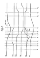
- FIG. 2 voltages at various points in the circuit 20 are shown plotted as a function of time to illustrate timing of circuit operation.
- the points are N1, C18, C27, N4, N2 and N3.
- Figure 2 is an idealised drawing intended to be indicative only and voltages are not to scale.
- the time (abscissa) axis is intended to be linear, but times given are approximate because of measurement difficulties for intervals of the order of nanoseconds.
- the mode of operation of the circuit 20 will now be described with reference to Figures 1 and 2. Individual voltage levels and time instants to be given are nominal, because they will vary due to component manufacturing tolerances.
- the circuit 20 is initially in a quiescent state with node N1 at a potential of -0.9 V. This arises from the potential divider formed by the combination of resistor 31 connected in series with the parallel arrangement of diode D3/resistor 34 and diode D4/resistor 36. The combination is connected between +5 V at 28 and -5 V at 32, and diodes D3 and D4 each drop approximately 0.45 V. Node N3 is at +0.45 V by virtue of forward biased diode D1.
- N1 is at -0.9 V as has been said, diode D2 is reversed biased.
- the APD experiences the potential difference between N1 and the supply 24; ie it experiences a reverse bias of 256.1 V, which is 6 V in excess of the voltage V BR required to cause breakdown in response to photon absorption.
- the non-inverting comparator inputs C12 and C22 are both 0.45 V below the N1 voltage (-0.9 V) since diodes D3 and D4 are forward biased; ie these inputs are at -1.35 V, above both VR1 (-1.38 V) and VR2 (-1.5 V).
- the second comparator inverting output C28 is at ECL logic low of -1.9 V.
- N2 is at -1.35 V
- diode D5 experiences a reverse bias of 0.55 V.
- the dead-time circuit output N4 is at an ECL logic high of -0.9 V, which provides for the first comparator C1 to be in an unlatched or enabled output state.
- the foregoing quiescent conditions correspond to times before t1 in Figure 2. These conditions begin to change in response to absorption of a photon by the APD 22. Photon absorption initiates a current avalanche in the APD 22, which begins to draw current from the +5 V supply 28 via the 1 Kohm resistor 31.
- the maximum reverse current through a typical APD is in the region of 50 ⁇ Amp, and consequently the voltage at N1 may fall by up to 50 mV due to additional current flowing in the 1 Kohm resistor 31.
- the voltage at N1 has fallen by 30 mV, that at N2 has fallen by a like amount and has become equal to VR1 (-1.38 V).
- the voltages at N1 and N2 continue to fall together, and that at N2 passes below VR1 changing the sign of the difference signal between the first comparator inputs C12 and C13.
- the first comparator outputs C17 and C18 consequently change state at t2 after a propagation delay of about 2 nanoseconds (t2-t1).
- t2-t1 the signal at C18 is shown in Figure 2, since that at C17 is merely the inverse.
- the time t2 marks the beginning of the transition at C18. The transition takes a finite time to complete; it is convenient to indicate its initiation, and a similar convention is employed for later transitions.
- the change of output state at t2 triggers the quench circuit 38 to switch, which takes node N3 down to a voltage towards that of the -15 V supply 40.
- the voltage at N3 begins to fall at t3, about 1 nanosecond after t2. This forwards biases diode D2, and eventually reduces the voltage at N1 by in the region of 7 V. Since the APD 22 at quiescence was biased only 6 V above breakdown, reduction in the N1 voltage by 7 V takes it below breakdown and quenches the current avalanche as will be described later.
- the initiation of the voltage fall at N3 reduces the voltage at N1 beyond the reduction caused by the APD current avalanche.
- the voltage at N2 falls further, and passes below VR2 (-1.5 V) at t4, about 1.5 nanoseconds after t3. It is emphasised that the voltages at N1 and N2 must fall from their quiescent levels by more than 150 mV to take N2 below VR2, whereas a current avalanche in the APD 22 can produce a reduction of up to 50 mV only.
- the dead-time circuit 48 responds to the negative edge voltage change at C27 by driving N4 down to -1.9 V (ECL logic low). This latches the first comparator outputs C17 and C18 at levels corresponding to the comparator input at the time of latching, ie the N2 > VR1 condition. The first comparator is accordingly disabled and unresponsive to any subsequent change in the N2 voltage until enabled later.
- the latched output state of the first comparator C1 becomes operative at t8, 2 nanoseconds after t6. Since as has been said this corresponds to N2 > VR1, the signal to the quench circuit 38 is low and the quench supply voltage 40 is isolated from N3. This terminates quenching of the APD 22 at t9, and the voltages at N1 and N3 begin to rise in response to recharging of the APD 22 via the 1 Kohm bias resistor 31.
- APD recharge increases the voltage at N1 above VR2 + VD4, where VD4 is the forward bias voltage (0.45 V) across diode D4.
- VD4 is the forward bias voltage (0.45 V) across diode D4.
- the internal time constant of the monostable dead-time circuit 48 elapses; this is preset to 14 nanoseconds, and is equal to t12-t7.
- the circuit 48 returns N4 to ECL logic high re-enabling the first comparator C1 and returning the circuit 20 to its initial quiescent state.
- the output signal from the circuit 20 is monitored at 42, where the output circuit 41 provides matching to a 50 ohm load.
- the signal indicating detection of a photon by the APD 22 is a pulse a few nanoseconds in width corresponding to the delay between quench and reset.
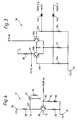
- the quench circuit 38 incorporates two fast switching npn transistors 60a and 60b type BFY90 (industry standard designation) arranged in a long-tailed pair differential amplifier configuration.
- the transistors 60a and 60b have base terminals 62a and 62b connected via 10 V zener diodes 64a and 64b to the first comparator's inverting and non-inverting outputs C18 and C17 (not shown) respectively.
- Transistor 60a has a collector connection to node N3 of Figure 1
- transistor 60b has a collector terminal 66 in series with a 270 ohm load resistor 68 connected to earth.
- the transistors have respective 330 ohm base bias resistors 70a and 70b and share a common 82 ohm emitter resistor 72 all connected to the -15 V supply 40.
- the output circuit 41 incorporates a fast switching npn output transistor 80 type BFY 90 having a base terminal 82 connected to the collector terminal 66 of the quench circuit 38.
- the base terminal 82 is connected to the -5 V supply 32 via a 180 ohm bias resistor 84 and a diode 86 type IN4149 arranged in series.
- the transistor 80 has a 10 Kohm collector resistor 88 and a 47 ohm emitter resistor 90, these being connected to +5 V and -5 V supplies 28 and 32 respectively.
- the output terminal 42 of the circuit 41 is connected to the collector connection 92 of the transistor 80.
- the output signal at 42 is matched to a 50 ohm load as indicated at 94.
- the quench and output circuits 38 and 41 operate as follows.
- the zener diodes 64a and 64b connect the outputs of the first comparator C1 to the quench circuit base terminals 62a and 62b. They introduce zener voltage offsets of 10 V between these points. These diodes however have very low dynamic impedances for coupling pulses to the base terminals 62a and 62b.
- comparator C1 changes output states in response to initiation of an APD avalanche, transistor bases 62a and 62b are pulsed high and low respectively. This switches transistor 60a on and transistor 60b off. Current is drawn from +5 V supply 28 through the series arrangement of resistor 31, diode D2, transistor 60a and emitter resistor 72 to -15 V supply 40.
- N3 In practice, the fall is arrested by termination of quench, which occurs in response to change in the first comparator output state. In the circuit 38 illustrated, N3 in fact falls by at least 8 V. In consequence, N1 in Figure 1 will be reduced by at least 6 V as required to quench the APD avalanche.
- transistor base 62b When transistor base 62b is pulsed low, its corresponding collector terminal goes high to near earth potential. This switches on the output transistor 80 producing a low voltage level at the output terminal 42.
- the collective response of the quench and output circuits 38 and 41 to an APD avalanche is therefore the production of a negative going pulse at the output terminal 42.
- the dead-time circuit 48 is illustrated in Figure 5. It incorporates a monostable circuit type MC10198 manufactured by Motorola Inc., an American company as has been said. It employs 0 V and -5 V power supplies and operates between ECL logic levels. The circuit will not be described in detail, since it is a standard configuration and component types and values are illustrated.
- the monostable circuit pulse width ⁇ t is a function of the values of a capacitor 100 and a variable resistor 102 (0 to 5 Kohm). The pulse width ⁇ t corresponds to the interval t12-t7 in Figure 2.
- ⁇ t 1.19C(R+284) seconds
- C value of capacitor 100 (Farads)
- ⁇ t or t12-t7 is variable from 3.4 nanoseconds to 63 nanoseconds for R in the range 0 to 5 Kohms.
- the total dead-time of the circuit 20 is ⁇ t added to t7-t1 and the time before t1 during which N1 falls to VR1 + 0.45 after photon absorption. The total dead-time is approximately 24 nanoseconds.
- the circuit 20 is therefore capable of detecting more than 4x10⁷ photons per second, a detection rate better than 40 MHz.
- the dead-time of the circuit 20 is only a little more than the fundamental limits set by the physical properties of the APD 22, in terms of response to quenching and speed of recovery and recharging.
- the photon-induced avalanche is detected very shortly after initiation, and the reset operation is implemented only when operation of the quench circuit is detected by the second comparator C2.
- the first comparator C1 is latched after reset, and is therefore reliably desensitised until the end of the monostable circuit time constant ⁇ t. This provides a reliable dead-time during which unwanted pulses cannot be output and enabling accurate computation of dead-time pulse count corrections. If faster photodiodes, transistors and comparators become available, the circuit 20 will automatically operate in a shorter time interval, and the monostable circuit time constant is all that requires adjustment to obtain shorter dead-time and higher detection rate.
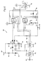
- FIG 6 there is shown an alternative embodiment 120 of the invention, this being equivalent to that illustrated in Figure 1 with modified comparator latching arrangements. Parts equivalent to those shown in Figure 1 are like-referenced with 100 prefixes or asterisk superscripts (eg C1*) as appropriate.
- the circuits 20 and 120 are very similar, and the following description will be directed to their differences.
- the circuit 120 differs to that described earlier only in that the dead-time circuit 148 receives input from the first comparator's inverting output C1 * 8 instead of that of the second comparator C2*. This has the following effect on circuit operation.
- the first comparator C1* is now latched in response to a change of state at its own output, and after the sum of the propagation delay through itself (2 nanoseconds) and the delay introduced by the dead-time circuit 148 (eg 14 nanoseconds).
- the relevant change of state is negative-going, since the dead-time circuit is negative edge triggered as described earlier.
- the first comparator's inverting output C1 * 8 produces a negative edge at t8 in Figure 2; this occurs in response to reset of the node N2, and corresponds to termination of the quench signal supplied to the quench circuit 138 by the first comparator C1*.
- the output node N4 of the dead-time circuit 148 changes state 2.5 nanoseconds after the negative edge is output from the first comparator C1* (which indicated this comparator's return to the non-quench state). This provides a latch signal at the first comparator latch input terminal C1 * 4 .
- the first comparator C1* consequently becomes latched in an output state corresponding to node N2 (first-comparator input C1 * 2 ) in a reset or non-quench state.
- the reason for the modification shown in Figure 6 is to avoid the possibility of the first comparator C1 becoming latched in the quench state, which would mean that the APD 122 would not recharge. This possibility could occur in the Figure 1 embodiment if the diode D5 and resistors 34 and 46 introduced a time constant which was longer than the propagation delay through the dead-time circuit 48.
- the Figure 6 device 120 does suffer from the disadvantage that a complete detection cycle is extended by the length of the propagation delay through the first comparator C1*, unless of course the dead-time circuit 148 is adjusted to compensate.
- a further point is that it is necessary for the first comparator to be latched before the second comparator changes state back to quiescence (t11 in Figure 2). This is easily satisfied in the circuits of Figures 1 and 6.
Landscapes
- Engineering & Computer Science (AREA)
- General Physics & Mathematics (AREA)
- Physics & Mathematics (AREA)
- Remote Sensing (AREA)
- Computer Networks & Wireless Communication (AREA)
- Radar, Positioning & Navigation (AREA)
- Spectroscopy & Molecular Physics (AREA)
- Photometry And Measurement Of Optical Pulse Characteristics (AREA)
- Measurement Of Current Or Voltage (AREA)
- Amplifiers (AREA)
- Light Receiving Elements (AREA)
- Electronic Switches (AREA)
- Solid State Image Pick-Up Elements (AREA)
Claims (5)
- Avalanche-Photodioden-Löschschaltung mit einer Avalanche-Photodiode (22), die über einen Lastwiderstand (31) wieder aufladbar ist, einem Avalanche-Nachweisverstärker (C1) mit einem Eingang (C1₂), der so geschaltet ist, daß er ein Signal von der Photodiode (22) empfängt, und so angeordnet ist, daß er auf eine Photodiodenlawine mit Aktivierung der Löschvorrichtung (38) reagiert, Reset-Vorrichtung (C2, D5, 34, 46) mit und gesteuert von einem zweiten Verstärker (C2), die so angeordnet ist, daß sie den Avalanche-Nachweisverstärker (C1) nach dem Nachweis einer Lawine zurücksetzt, und Vorrichtung für die Einführung einer Schaltungstotzeit (48),
dadurch gekennzeichnet, daß
der besagte zweite Verstärker (C2) so angeordnet ist, daß er auf ein Absinken der Photodiodenvorspannung aufgrund der Auslösung der Löschung reagiert. - Schaltung nach Anspruch 1,
dadurch gekennzeichnet, daß
die Vorrichtung für Einführung einer Schaltungstotzeit eine Verriegelungsvorrichtung (48) umfaßt, die durch den zweiten Verstärker (C2) zum Verriegeln der Ausgangsantwort des Avalanche-Nachweisverstärkers (C1) auf den Eingangs-Reset gesteuert wird. - Schaltung nach Anspruch 2,
dadurch gekennzeichnet, daß
die Verriegelungsvorrichtung eine monostabile Schaltung (48) umfaßt, die durch eine Zustandsänderung des zweiten Verstärkerausgangs (C2₇) triggerbar ist. - Schaltung nach Anspruch 1,
dadurch gekennzeichnet, daß
die Vorrichtung für die Einführung einer Schaltungstotzeit eine monostabile Schaltung (148) umfaßt, die durch Zustandsänderung des Ausgangs (C1₈*) des Avalanche-Nachweisverstärkers (C1*) triggerbar ist. - Schaltung nach Anspruch 2, 3 oder 4,
dadurch gekennzeichnet, daß
die Löschvorrichtung einen Differenzverstärker (60a, 60b) umfaßt, der mit dem Avalanche-Nachweisverstärkerausgang (C1₇, C1₈) verbunden ist und der nach Aktivierung das Absenken des Avalanche-Photodiodenpotentials verringert.
Applications Claiming Priority (3)
| Application Number | Priority Date | Filing Date | Title |
|---|---|---|---|
| GB898915245A GB8915245D0 (en) | 1989-07-03 | 1989-07-03 | Avalanche photodiode quenching circuit |
| GB8915245 | 1989-07-03 | ||
| PCT/GB1990/001012 WO1991000502A1 (en) | 1989-07-03 | 1990-07-02 | Avalanche photodiode quenching circuit |
Publications (2)
| Publication Number | Publication Date |
|---|---|
| EP0481016A1 EP0481016A1 (de) | 1992-04-22 |
| EP0481016B1 true EP0481016B1 (de) | 1994-05-25 |
Family
ID=10659468
Family Applications (1)
| Application Number | Title | Priority Date | Filing Date |
|---|---|---|---|
| EP90917799A Expired - Lifetime EP0481016B1 (de) | 1989-07-03 | 1990-07-02 | Erlöschungsschaltung für lawinenfotodioden |
Country Status (8)
| Country | Link |
|---|---|
| US (1) | US5194727A (de) |
| EP (1) | EP0481016B1 (de) |
| JP (1) | JP2750000B2 (de) |
| AT (1) | ATE106139T1 (de) |
| CA (1) | CA2060658C (de) |
| DE (1) | DE69009188T2 (de) |
| GB (1) | GB8915245D0 (de) |
| WO (1) | WO1991000502A1 (de) |
Cited By (1)
| Publication number | Priority date | Publication date | Assignee | Title |
|---|---|---|---|---|
| WO2021178434A1 (en) * | 2020-03-04 | 2021-09-10 | The University Of Chicago | Avalanche photodiodes with adaptive quenching of photocurrent |
Families Citing this family (21)
| Publication number | Priority date | Publication date | Assignee | Title |
|---|---|---|---|---|
| GB2269010B (en) * | 1992-07-25 | 1996-01-17 | Roke Manor Research | Improvements in or relating to photon counters |
| JP2686036B2 (ja) * | 1993-07-09 | 1997-12-08 | 浜松ホトニクス株式会社 | アバランシェフォトダイオードのバイアス回路 |
| US5532474A (en) * | 1993-12-17 | 1996-07-02 | Eg&G Limited | Active quench circuit and reset circuit for avalanche photodiode |
| US5933042A (en) * | 1997-07-01 | 1999-08-03 | Eg&G Canada, Ltd. | Active quench circuit for an avalanche current device |
| KR100308216B1 (ko) * | 1999-03-15 | 2001-09-26 | 윤종용 | 밀봉된 전자기기의 비인가된 개봉을 검출하는 장치 |
| US6424375B1 (en) * | 1999-09-21 | 2002-07-23 | Pixel Devices, International | Low noise active reset readout for image sensors |
| IT1316793B1 (it) * | 2000-03-09 | 2003-05-12 | Milano Politecnico | Circuito monolitico di spegnimento attivo e ripristino attivo perfotodiodi a valanga |
| CN100363724C (zh) * | 2004-02-24 | 2008-01-23 | 华东师范大学 | 双门控雪崩光电二极管单光子探测方法 |
| CN100410636C (zh) * | 2004-03-19 | 2008-08-13 | 华东师范大学 | 一种apd单光子探测的电路模块 |
| JP5266785B2 (ja) * | 2008-02-19 | 2013-08-21 | 富士通株式会社 | 光検出装置および光検出方法 |
| US8803075B2 (en) * | 2008-04-18 | 2014-08-12 | Saint-Gobain Ceramics & Plastics, Inc. | Radiation detector device |
| CN101923173B (zh) * | 2009-06-10 | 2014-10-01 | 圣戈本陶瓷及塑料股份有限公司 | 闪烁体以及检测器组件 |
| GB2485995B (en) * | 2010-11-30 | 2014-01-01 | St Microelectronics Res & Dev | Improved proximity sensor and associated method, computer readable medium and firmware |
| US9671284B1 (en) * | 2016-01-14 | 2017-06-06 | Kiskeya Microsystems Llc | Single-photon avalanche diode circuit with variable hold-off time and dual delay regime |
| CN106482840B (zh) * | 2016-09-27 | 2019-03-08 | 山东大学 | 一种用于单光子探测器的主动猝灭电路及其工作方法 |
| EP3309582B1 (de) * | 2016-10-12 | 2022-12-07 | STMicroelectronics (Research & Development) Limited | Auf einzelphotonen-lawinendioden basierende bereichserkennungsvorrichtung |
| JP7278821B2 (ja) * | 2019-03-22 | 2023-05-22 | 株式会社東芝 | センサ及び距離計測装置 |
| EP3999821B1 (de) * | 2019-07-19 | 2025-01-08 | Avago Technologies International Sales Pte. Limited | Ladeschaltung für digitale silizium-photovervielfacher |
| CN113138019B (zh) * | 2021-03-23 | 2022-04-15 | 北京大学 | 一种基于雪崩光电二极管阵列的读出电路和光电探测器 |
| JP7755168B2 (ja) * | 2022-09-22 | 2025-10-16 | 株式会社デンソーウェーブ | 距離計測装置 |
| CN116558654A (zh) * | 2023-05-12 | 2023-08-08 | 中南民族大学 | 一种新型的单光子雪崩二极管淬灭和读出电路 |
Family Cites Families (4)
| Publication number | Priority date | Publication date | Assignee | Title |
|---|---|---|---|---|
| US4754131A (en) * | 1985-12-31 | 1988-06-28 | American Telephone And Telegraph Company, At&T Bell Laboratories | Devices using avalanche photodiode and capable of detecting a small number of photons |
| ATE78587T1 (de) * | 1986-11-25 | 1992-08-15 | Secr Defence Brit | Quench-schaltung fuer avalanche-photodioden. |
| IT1229945B (it) * | 1988-10-20 | 1991-09-17 | Consiglio Nazionale Ricerche | Circuito di spegnimento attivo per fotodiodi a semiconduttore a valanga per singoli fotoni, adatto per il funzionamento con fotodiodo in posizione remota |
| DE4006504A1 (de) * | 1990-03-02 | 1991-09-05 | Telefunken Electronic Gmbh | Schaltungsanordnung fuer opto-schmitt-trigger |
-
1989
- 1989-07-03 GB GB898915245A patent/GB8915245D0/en active Pending
-
1990
- 1990-07-02 DE DE69009188T patent/DE69009188T2/de not_active Expired - Fee Related
- 1990-07-02 JP JP2509429A patent/JP2750000B2/ja not_active Expired - Lifetime
- 1990-07-02 CA CA002060658A patent/CA2060658C/en not_active Expired - Fee Related
- 1990-07-02 AT AT90917799T patent/ATE106139T1/de not_active IP Right Cessation
- 1990-07-02 EP EP90917799A patent/EP0481016B1/de not_active Expired - Lifetime
- 1990-07-02 US US07/834,287 patent/US5194727A/en not_active Expired - Lifetime
- 1990-07-02 WO PCT/GB1990/001012 patent/WO1991000502A1/en not_active Ceased
Cited By (1)
| Publication number | Priority date | Publication date | Assignee | Title |
|---|---|---|---|---|
| WO2021178434A1 (en) * | 2020-03-04 | 2021-09-10 | The University Of Chicago | Avalanche photodiodes with adaptive quenching of photocurrent |
Also Published As
| Publication number | Publication date |
|---|---|
| CA2060658A1 (en) | 1991-01-04 |
| EP0481016A1 (de) | 1992-04-22 |
| DE69009188T2 (de) | 1994-09-15 |
| ATE106139T1 (de) | 1994-06-15 |
| CA2060658C (en) | 1999-09-14 |
| JPH04506570A (ja) | 1992-11-12 |
| JP2750000B2 (ja) | 1998-05-13 |
| WO1991000502A1 (en) | 1991-01-10 |
| DE69009188D1 (de) | 1994-06-30 |
| US5194727A (en) | 1993-03-16 |
| GB8915245D0 (en) | 1989-08-23 |
Similar Documents
| Publication | Publication Date | Title |
|---|---|---|
| US5194727A (en) | Avalanche photodiode quenching circuit wtih resetting means having a second amplifier | |
| EP0333751B1 (de) | Quench-schaltung für avalanche-photodioden | |
| US5532474A (en) | Active quench circuit and reset circuit for avalanche photodiode | |
| KR100186820B1 (ko) | 레이저 도달 거리 파인더 장치 및 이러한 장치에서의 주파수 응답 측정 방법 | |
| EP1132724B1 (de) | Schaltung zur hochpräzisen Ermittlung der Ankunftszeit von Photonen auf durch einzelne Photonen getriggerte Avalanche-Dioden | |
| KR100186821B1 (ko) | 레이저 거리 측정 수신기 | |
| Cova et al. | 20‐ps timing resolution with single‐photon avalanche diodes | |
| Gallivanoni et al. | Progress in quenching circuits for single photon avalanche diodes | |
| US6218657B1 (en) | System for gated detection of optical pulses containing a small number of photons using an avalanche photodiode | |
| JP2017026615A (ja) | ガイガーモードのアバランシェフォトダイオードを有する受光器及び読み出し方法 | |
| JP2005510883A (ja) | フォトン計数応用のためのアバランシェフォトダイオードおよび単一フォトン検出システム | |
| Acerbi et al. | Fast active quenching circuit for reducing avalanche charge and afterpulsing in InGaAs/InP single-photon avalanche diode | |
| CN111656219B (zh) | 用于使用光信号确定至少一个对象的距离的装置和方法 | |
| US4505582A (en) | Self-detecting optical sensors | |
| EP1329700A1 (de) | Optische messvorrichtung und verfahren zur optischen messung | |
| US5322995A (en) | Charge integration preamplifier for use in radiation detection circuitry | |
| US4939476A (en) | Laser Rangefinder receiver preamplifier | |
| US4754131A (en) | Devices using avalanche photodiode and capable of detecting a small number of photons | |
| Lacaita et al. | Performance optimization of active quenching circuits for picosecond timing with single photon avalanche diodes | |
| Robinson et al. | Photon detection with cooled avalanche photodiodes | |
| Achtenberg et al. | Optical pulse monitoring unit for Free Space Optics | |
| Rai et al. | A picosecond optical pulse generator to calibrate the optical streak camera | |
| US5003168A (en) | Trigger circuit for a streak camera sweep drive circuit | |
| US4985628A (en) | Inspection apparatus incorporating digital electron detection | |
| Robinson et al. | A cooled avalanche photodiode with high photon detection probability |
Legal Events
| Date | Code | Title | Description |
|---|---|---|---|
| PUAI | Public reference made under article 153(3) epc to a published international application that has entered the european phase |
Free format text: ORIGINAL CODE: 0009012 |
|
| 17P | Request for examination filed |
Effective date: 19920120 |
|
| AK | Designated contracting states |
Kind code of ref document: A1 Designated state(s): AT BE CH DE FR GB IT LI NL SE |
|
| 17Q | First examination report despatched |
Effective date: 19930419 |
|
| GRAA | (expected) grant |
Free format text: ORIGINAL CODE: 0009210 |
|
| ITF | It: translation for a ep patent filed | ||
| AK | Designated contracting states |
Kind code of ref document: B1 Designated state(s): AT BE CH DE FR GB IT LI NL SE |
|
| REF | Corresponds to: |
Ref document number: 106139 Country of ref document: AT Date of ref document: 19940615 Kind code of ref document: T |
|
| REF | Corresponds to: |
Ref document number: 69009188 Country of ref document: DE Date of ref document: 19940630 |
|
| ET | Fr: translation filed | ||
| EAL | Se: european patent in force in sweden |
Ref document number: 90917799.0 |
|
| PLBE | No opposition filed within time limit |
Free format text: ORIGINAL CODE: 0009261 |
|
| STAA | Information on the status of an ep patent application or granted ep patent |
Free format text: STATUS: NO OPPOSITION FILED WITHIN TIME LIMIT |
|
| 26N | No opposition filed | ||
| REG | Reference to a national code |
Ref country code: GB Ref legal event code: 732E |
|
| BECA | Be: change of holder's address |
Free format text: 20011123 *QINETIQ LTD:85 BUCKINGHAM GATE, LONDON SW14 0LX |
|
| REG | Reference to a national code |
Ref country code: GB Ref legal event code: IF02 |
|
| PGFP | Annual fee paid to national office [announced via postgrant information from national office to epo] |
Ref country code: AT Payment date: 20020606 Year of fee payment: 13 |
|
| PGFP | Annual fee paid to national office [announced via postgrant information from national office to epo] |
Ref country code: FR Payment date: 20020610 Year of fee payment: 13 |
|
| PGFP | Annual fee paid to national office [announced via postgrant information from national office to epo] |
Ref country code: GB Payment date: 20020612 Year of fee payment: 13 |
|
| PGFP | Annual fee paid to national office [announced via postgrant information from national office to epo] |
Ref country code: SE Payment date: 20020617 Year of fee payment: 13 Ref country code: CH Payment date: 20020617 Year of fee payment: 13 |
|
| PGFP | Annual fee paid to national office [announced via postgrant information from national office to epo] |
Ref country code: NL Payment date: 20020619 Year of fee payment: 13 Ref country code: DE Payment date: 20020619 Year of fee payment: 13 |
|
| REG | Reference to a national code |
Ref country code: FR Ref legal event code: TP |
|
| PGFP | Annual fee paid to national office [announced via postgrant information from national office to epo] |
Ref country code: BE Payment date: 20020724 Year of fee payment: 13 |
|
| NLS | Nl: assignments of ep-patents |
Owner name: QINETIQ LIMITED |
|
| PG25 | Lapsed in a contracting state [announced via postgrant information from national office to epo] |
Ref country code: GB Free format text: LAPSE BECAUSE OF NON-PAYMENT OF DUE FEES Effective date: 20030702 Ref country code: AT Free format text: LAPSE BECAUSE OF NON-PAYMENT OF DUE FEES Effective date: 20030702 |
|
| PG25 | Lapsed in a contracting state [announced via postgrant information from national office to epo] |
Ref country code: SE Free format text: LAPSE BECAUSE OF NON-PAYMENT OF DUE FEES Effective date: 20030703 |
|
| PG25 | Lapsed in a contracting state [announced via postgrant information from national office to epo] |
Ref country code: LI Free format text: LAPSE BECAUSE OF NON-PAYMENT OF DUE FEES Effective date: 20030731 Ref country code: CH Free format text: LAPSE BECAUSE OF NON-PAYMENT OF DUE FEES Effective date: 20030731 Ref country code: BE Free format text: LAPSE BECAUSE OF NON-PAYMENT OF DUE FEES Effective date: 20030731 |
|
| BERE | Be: lapsed |
Owner name: *QINETIQ LTD Effective date: 20030731 |
|
| PG25 | Lapsed in a contracting state [announced via postgrant information from national office to epo] |
Ref country code: NL Free format text: LAPSE BECAUSE OF NON-PAYMENT OF DUE FEES Effective date: 20040201 |
|
| PG25 | Lapsed in a contracting state [announced via postgrant information from national office to epo] |
Ref country code: DE Free format text: LAPSE BECAUSE OF NON-PAYMENT OF DUE FEES Effective date: 20040203 |
|
| GBPC | Gb: european patent ceased through non-payment of renewal fee |
Effective date: 20030702 |
|
| EUG | Se: european patent has lapsed | ||
| REG | Reference to a national code |
Ref country code: CH Ref legal event code: PL |
|
| PG25 | Lapsed in a contracting state [announced via postgrant information from national office to epo] |
Ref country code: FR Free format text: LAPSE BECAUSE OF NON-PAYMENT OF DUE FEES Effective date: 20040331 |
|
| NLV4 | Nl: lapsed or anulled due to non-payment of the annual fee |
Effective date: 20040201 |
|
| REG | Reference to a national code |
Ref country code: FR Ref legal event code: ST |
|
| PG25 | Lapsed in a contracting state [announced via postgrant information from national office to epo] |
Ref country code: IT Free format text: LAPSE BECAUSE OF NON-PAYMENT OF DUE FEES;WARNING: LAPSES OF ITALIAN PATENTS WITH EFFECTIVE DATE BEFORE 2007 MAY HAVE OCCURRED AT ANY TIME BEFORE 2007. THE CORRECT EFFECTIVE DATE MAY BE DIFFERENT FROM THE ONE RECORDED. Effective date: 20050702 |