EP0479305B1 - Rate conversion apparatus - Google Patents
Rate conversion apparatus Download PDFInfo
- Publication number
- EP0479305B1 EP0479305B1 EP91116952A EP91116952A EP0479305B1 EP 0479305 B1 EP0479305 B1 EP 0479305B1 EP 91116952 A EP91116952 A EP 91116952A EP 91116952 A EP91116952 A EP 91116952A EP 0479305 B1 EP0479305 B1 EP 0479305B1
- Authority
- EP
- European Patent Office
- Prior art keywords
- signal
- phase
- frequency
- periodical
- output
- Prior art date
- Legal status (The legal status is an assumption and is not a legal conclusion. Google has not performed a legal analysis and makes no representation as to the accuracy of the status listed.)
- Expired - Lifetime
Links
Images

Classifications
-
- H—ELECTRICITY
- H03—ELECTRONIC CIRCUITRY
- H03L—AUTOMATIC CONTROL, STARTING, SYNCHRONISATION, OR STABILISATION OF GENERATORS OF ELECTRONIC OSCILLATIONS OR PULSES
- H03L7/00—Automatic control of frequency or phase; Synchronisation
- H03L7/06—Automatic control of frequency or phase; Synchronisation using a reference signal applied to a frequency- or phase-locked loop
- H03L7/16—Indirect frequency synthesis, i.e. generating a desired one of a number of predetermined frequencies using a frequency- or phase-locked loop
-
- H—ELECTRICITY
- H03—ELECTRONIC CIRCUITRY
- H03L—AUTOMATIC CONTROL, STARTING, SYNCHRONISATION, OR STABILISATION OF GENERATORS OF ELECTRONIC OSCILLATIONS OR PULSES
- H03L7/00—Automatic control of frequency or phase; Synchronisation
- H03L7/06—Automatic control of frequency or phase; Synchronisation using a reference signal applied to a frequency- or phase-locked loop
- H03L7/08—Details of the phase-locked loop
- H03L7/099—Details of the phase-locked loop concerning mainly the controlled oscillator of the loop
- H03L7/0991—Details of the phase-locked loop concerning mainly the controlled oscillator of the loop the oscillator being a digital oscillator, e.g. composed of a fixed oscillator followed by a variable frequency divider
-
- H—ELECTRICITY
- H04—ELECTRIC COMMUNICATION TECHNIQUE
- H04L—TRANSMISSION OF DIGITAL INFORMATION, e.g. TELEGRAPHIC COMMUNICATION
- H04L25/00—Baseband systems
- H04L25/02—Details ; arrangements for supplying electrical power along data transmission lines
- H04L25/05—Electric or magnetic storage of signals before transmitting or retransmitting for changing the transmission rate
-
- H—ELECTRICITY
- H03—ELECTRONIC CIRCUITRY
- H03L—AUTOMATIC CONTROL, STARTING, SYNCHRONISATION, OR STABILISATION OF GENERATORS OF ELECTRONIC OSCILLATIONS OR PULSES
- H03L2207/00—Indexing scheme relating to automatic control of frequency or phase and to synchronisation
- H03L2207/10—Indirect frequency synthesis using a frequency multiplier in the phase-locked loop or in the reference signal path
Definitions
- the present invention relates to a technique for converting a data sequence of a transmission rate f1 to another data sequence of another transmission rate f2, and more particularly to a rate conversion apparatus for generating from clock signals of a frequency f1 clock signals of another frequency f2.
- the signal transmission rate is often converted in communication systems, and conversion is frequently accomplished from a signal transmission rate of f1 (samples/sec) into another transmission rate f2 which is equal to n/m times (m and n are mutually prime natural numbers) f1.
- data received over a line whose transmission rate is f1 are sent out over another line whose transmission rate is f2, which is not equal to f1.
- data of f1 in transmission rate are subjected to error detection coding or error correction coding to be converted into data of f2 in transmission rate (f1 ⁇ f2 in this case).
- this frequency synthesizer is composed of an m frequency divider for frequency-dividing signals of the frequency f1 by m and a PLL to which the output of the m frequency divider is supplied.
- the PLL further consists of a phase comparator whose first input terminal is supplied with the output of the m frequency divider, a loop filter for filtering the output of the phase comparator, a voltage controlled oscillator (VCO) whose oscillation frequency varies around a center frequency of f2 according to the output of the loop filter, and the n frequency divider for frequency-dividing the output of the VCO by n and supplying the n frequency-divided output to a second terminal of the phase comparator.
- VCO voltage controlled oscillator
- the band-width of the loop filter should be sufficiently narrower than 8 kHz, for example, around 1 kHz.
- the pull-in time of the PLL in this instance will be about 1 msec, an undesirably long pull-in time.
- An object of the present invention is to provide a rate conversion apparatus taking short pull-in time irrespective of the n/m ratio between a first frequency f1 and a second frequency f2 and permitting ready realization of appropriate circuitry. This object is solved with the features of the claims.
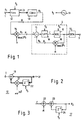
- FIG. 1 is a block diagram illustrating a first preferred embodiment of the invention.
- This embodiment involves a digital tank circuit 12 which is supplied with a first clock signal of f1 in frequency and supplies a complex signal, a read-only memory (ROM) 13 for converting the complex signal into an R-bit signal ⁇ 1 indicating the phase of the first clock signal, and a multiplier 14 for multiplying the phase signal ⁇ 1 by n (modulo 2 R ).
- ROM read-only memory
- This embodiment is also provided with a digital phase lock loop (PLL) 2 comprising a subtractor 15, a digital low-pass filter (LPF) 16, a numerically controlled oscillator (NCO) 17, and a multiplier 18 for multiplying the output of the NCO 17 by m (modulo 2 R ), wherein the NCO 17 supplies another phase signal ⁇ 2 indicating the phase of a second clock signal of f2 in frequency.
- the embodiment further involves a clock source 11 for supplying an operation clock of fs in frequency to the digital tank circuit 12, the LPF 16 and the NCO 17, and a clock generating circuit 10 for converting the signal ⁇ 2, which is supplied by the NCO 17, into the second clock signal.
- the frequency fs of the operation clock is determined by the level of accuracy required for the waveform of the second clock signal, and about 32 times the frequency f1 or f2, whichever is higher, is usually sufficient as fs.
- the first clock signal of f1 in frequency is supplied to the digital tank circuit 12, which extracts, an the basis of the operation clock from a clock generator, only the frequency f1 component from the first clock signal and, at the same time, converts the first clock signal into the complex signal x+jy whose phase angle indicates the phase of the first clock signal.
- the configuration of this digital tank circuit 12 will be described later in further detail.
- This complex signal is further converted by a converting circuit or the read only memory 13 into the first phase signal ⁇ 1, i.e. a signal indicating the phase of the first clock signal.
- This converting circuit 13 can be composed of a read-only memory (ROM), having the real and imaginary parts of the complex signal as addresses and a phase angle stored in each address.
- This first phase signal ⁇ 1 is represented by an R-bit digital signal.
- the first clock signal entered from a terminal 1 is thus converted into the first phase signal ⁇ 1 indicating the phase of the first clock signal.
- This first phase signal ⁇ 1 is n-multiplied by the mudulo 2 R multiplier 14 into n ⁇ 1 (mod 2 R ).
- the multiplier 14 supplies a third phase signal ⁇ 3 (R-bit) indicating the phase of a cyclic signal of nf1 in frequency, resulting from the n-multiplication of the first clock signal of fl in frequency, to the digital PLL 2.
- phase error signal ⁇ 3 is subtracted a fourth phase signal ⁇ 4 by the subtractor 15 to give a phase error signal.
- This phase error signal is smoothed by the LPF 16 into a smoothed phase error signal C.
- the NCO 17 supplies the phase signal ⁇ 2 to control the frequency and phase of the second clock signal, which is supplied from a clock generating circuit 10, on the basis of the smoothed phase error signal C and the operation clock.
- This phase signal ⁇ 2 thus represents the phase of the second clock signal.
- the configuration of the NCO 17 will be described later in further detail.
- the clock generating circuit 10 is supplied with the phase signal ⁇ 2 and supplies the second clock signal of f2 in frequency.
- This clock generating circuit 10 can be composed of a read-only memory in which amplitude values are stored correspondingly to phase signals. If a rectangular wave is required as the second clock signal, the most significant bit or the R-bit phase signal ⁇ 2 may as well be extracted and used as the second clock signal as it is.
- the phase signal ⁇ 2 is also supplied to the multiplier 18, which multiplies this phase signal ⁇ 2 by m (modulo 2 R ) into the fourth phase signal ⁇ 4.
- This fourth phase signal ⁇ 4 represents the phase of the periodic signal of mf2 in frequency, obtained by multiplying the second clock signal of f2 in frequency by m.
- the fourth phase signal ⁇ 4 is subtracted from the third phase signal ⁇ 3 by the subtractor 15 to give a phase error signal ( ⁇ 3 - ⁇ 4), which, as mentioned above, is supplied to the LPF 16.
- phase signal ⁇ 4 is phase-synchronized with the phase signal ⁇ 3.
- This is equivalent to the phase-synchronism between the periodical signal of nf1 in frequency corresponding to the phase signal ⁇ 3 and the periodical signal of mf2 in frequency corresponding to the phase signal ⁇ 4. Therefore, the function of this preferred embodiment is equivalent to the second method described previously.
- the operation of the preferred embodiment illustrated in FIG. 1 takes place wholly at the timings set by the operation clock fs.
- the frequency fs of this operation clock will be high enough if it is about 32 times the frequency fl or f2 whichever is the higher.
- fs may be about 65 MHz.
- the invention is free from the disadvantage of the second method described previously that the input frequency of the phase comparator becomes too high for ready production of the PLL.
- the operation rate of the digital PLL is relatively high, about 65 MHz, the bandwidth of the PLL, even if it is selected at 1/8 of fs, will be about 8 MHz. Therefore the pull-in action of the PLL will be quick enough to enable the disadvantage of the aforementioned first method to be overcome.
- the digital tank circuit 12 is provided with an adder 19, a one-sample delay circuit (Z -1 ) 20 and a multiplier 21.
- the one-sample delay circuit is supplied with the operation clock (fs).
- the digital tank circuit 12 is tuned to the frequency f1 and operates as a single-tuned circuit of ⁇ (1 - ⁇ )fs/2 ⁇ Hz in bandwidth.
- the digital tank circuit 12 is also a complex signal processing circuit, and the complex signal x + jy, which is its output, is a signal whose phase angle indicates the phase of the first clock signal.
- the NCO 17 is provided with adders 22 and 23 and a one-sample delay circuit 24. All these adders 22 and 23 and one-sample delay circuit 24 are binary R-bit digital signal processing circuits.
- the NCO 17 serves as a sort of oscillator.
- phase of the NCO 17 will be controlled by the phase control signal C.
- the first preferred embodiment of the present invention can make up a rate conversion apparatus capable of quick pull-in without having to make the PLL operate at an extremely high frequency even if the values of m and n are great.
- (n ⁇ 1 - m ⁇ 2) mod2 R to be supplied to the LPF 16 is represented by the following equation.
- (n ⁇ 1 - m ⁇ 2) mod2 R (n1 ⁇ 1 - m1 ⁇ 2) mod2 R + (n2 ⁇ 1 - m2 ⁇ 2) mod2 R + (n3 ⁇ 1 - m3 ⁇ 2) mod2 R + (n4 ⁇ 1 - m4 ⁇ 2) mod2 R Since every one of the numbers n1 through n4 and ml through m4 in Equation (5) is a prime number, in the modulo 2 R arithmetic operation, not all of the terms will identically give zero.
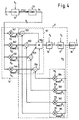
- FIG. 4 is a block diagram illustrating a second preferred embodiment of the present invention, which differs from the embodiment shown in FIG. 1 in the following three respects.
- the multipliers 141 through 144 perform the operations of n1 ⁇ 1(mod 2 R ), n2 ⁇ 1(mod 2 R ), n3 ⁇ 1(mod 2 R ) and n4 ⁇ 1(mod 2 R ), respectively.
- the multipliers 181 through 184 perform the operations of m1 ⁇ 2(mod 2 R ), m2 ⁇ 2(mod 2 R ), m3 ⁇ 2(mod 2 R ) and m4 ⁇ 2(mod 2 R ), respectively.
- the subtractors 151 through 154 perform the operations of (n1 ⁇ 1 - m1 ⁇ 2) (mod 2 R ), (n2 ⁇ 1 - m2 ⁇ 2) (mod 2 R ), (n3 ⁇ 1 - m302) (mod 2 R ), (n4 ⁇ 1 - m4 ⁇ 2) (mod 2 R ), respectively.
- the results of these operations are added by the adder 150 to perform the operation of Equation (5).
- Either the first or the second preferred embodiment of the present invention described above can constitute a rate conversion apparatus capable of quick pull-in without having to make the PLL operate at an extremely high frequency even if the values of m and n are great.
- both the first and the second embodiments require an operation clock frequency fs equal to about 32 times f1 or f2 whichever is the higher because of the necessity to ensure a sufficiently high level of time accuracy for the output waveform of the clock generator 10. Therefore, if the values of f1 and f2 are extremely high, that of fs will be correspondingly high to make it difficult to realize the circuitry.
- a third preferred embodiment of the invention to be described below with reference to FIG. 5, solves this problem.
- the first and third embodiments differ from each other in that the latter has a hybrid configuration while the former has a wholly digital configuration.
- the complex digital tank circuit 12 in FIG. 1 is replaced with a complex signal generating circuit 30.
- the digital PLL 2, too, is replaced with a PLL 2' having a partly analog configuration.
- a complex signal generating circuit 30 consists of an analog tank circuit 31, a phase shifter 32 and analog-to-digital (A/D) converters 33 and 34.
- the analog tank circuit 31 is tuned to the frequency f1 of the input clock signal, and outputs a sine wave phase-synchronized with the input clock signal. Incidentally, if the input clock signal is entered from the input terminal 1 as a sine wave, this analog tank circuit 31 can be dispensed with.
- the sine wave of f1 in frequency outputted from the analog tank circuit 31 is supplied to the A/D converter 33.
- the output of the A/D converter 33 is a signal identical with the real part x of the complex signal x + jy referred to in FIG. 1.
- the output of the analog tank circuit 31 is also supplied to the phase shifter 32 to be shifted in phase by ⁇ /2.
- This ⁇ /2 phase-shifted signal is digitalized by the A/D converter 34, and constitutes the imaginary part 6 of the complex signal x + jy referred to in FIG. 1.
- These signals x and y are supplied to the ROM 13 to give the first phase signal ⁇ 1 as in the first preferred embodiment.
- This first phase signal ⁇ 1 is multiplied by n (mod 2 R ) by the multiplier 14 into the third phase signal ⁇ 3. From this third phase signal ⁇ 3 is subtracted the fourth phase signal ⁇ 4, which is supplied by the multiplier 18, by the subtractor 15 to give the phase error signal, as in the first preferred embodiment.
- this phase error signal is converted by a digital-to-analog (D/A) converter 35 into an analog signal and outputted as an analog phase error signal.
- the analog phase error signal is filtered by an LPF 36 and supplied to a VCO 37 to control the oscillating frequency and phase of the VCO 37, from which a second clock signal of f2 in frequency is supplied.
- This second clock signal is converted by A/D converters 39 and 40 and a phase shifter 38 into a complex signal (x' + jy') whose phase angle indicates the phase of the second clock signal, and further converted by an ROM 41 into a second phase signal ⁇ 2.
- the operation of the circuit consisting of these A/D converters 39 and 40, phase shifter 38 and ROM 41 is the same as that of the circuit comprising the A/D converters 33 and 34, phase shifter 32 and ROM 13. If the output of the VCO 37 is a rectangular wave, there will be required an analog tank circuit tuned to the frequency f2 immediately at the coupling point between the input to the A/D converter 39 and that to the phase shifter 38.
- the second phase signal ⁇ 2 is multiplied by m (mod 2 R ) by the multiplier 18 and supplied as a fourth phase signal to the subtractor 15. In this way, the clock signal of f1 in frequency is converted into another clock signal of f2 in frequency.
- the present invention makes it possible to realize rate conversion of n/m in conversion ratio without having to set the operation frequency of the PLL extremely high or to reduce the equivalent bandwidth of the PLL even if the values of m and n are high. This results in the benefit of quicker pull-in, and the consequent freedom from the influence of the values of m and n enables the rate conversion apparatus according to the invention to be extensively applied to communications systems.
Description
- The present invention relates to a technique for converting a data sequence of a transmission rate f1 to another data sequence of another transmission rate f2, and more particularly to a rate conversion apparatus for generating from clock signals of a frequency f1 clock signals of another frequency f2.
- The signal transmission rate is often converted in communication systems, and conversion is frequently accomplished from a signal transmission rate of f1 (samples/sec) into another transmission rate f2 which is equal to n/m times (m and n are mutually prime natural numbers) f1.
- In one of the cases well known to persons skilled in the art where such processing takes place, data received over a line whose transmission rate is f1 are sent out over another line whose transmission rate is f2, which is not equal to f1. In another instance, data of f1 in transmission rate are subjected to error detection coding or error correction coding to be converted into data of f2 in transmission rate (f1 < f2 in this case).
- What is needed here is to generate another clock signals of another frequency f2 from a clock signal of a frequency f1. For this purpose, a frequency synthesizer using a phase-locked loop (PLL) is often used. For details on such a frequency synthesizer using a PLL, reference may be made to F.M. Gardner, Phaselock Techniques (1979, John Wiley & Sons, Inc.), pp. 208-214.
- In the presence of a relationship of nf1 = mf2 (m and n are mutually prime integers) between the frequencies f1 and f2, this frequency synthesizer is composed of an m frequency divider for frequency-dividing signals of the frequency f1 by m and a PLL to which the output of the m frequency divider is supplied. The PLL further consists of a phase comparator whose first input terminal is supplied with the output of the m frequency divider, a loop filter for filtering the output of the phase comparator, a voltage controlled oscillator (VCO) whose oscillation frequency varies around a center frequency of f2 according to the output of the loop filter, and the n frequency divider for frequency-dividing the output of the VCO by n and supplying the n frequency-divided output to a second terminal of the phase comparator. According to the prior art, clock signals of the frequency f1 are converted into clock signals of the frequency f2 in this manner. In this case, the frequency Δf of the signals entered into the two inputs of the phase comparator is equal to


- Incidentally, m and n sometimes may be very large numbers. If, for instance, f1 is 1.544 MHz and f2, 2.048 MHz, m will be 193 and n, 256, and in this case the frequency Δf of the input signals of the phase comparator in the PLL would be equal to


- A conceivable solution to this problem, according to the prior art, is to replace the n frequency divider with an m times multiplier and the m frequency divider in the PLL with an n time multiplier to make the frequency f0 of the two signals to be compared by the phase comparator equal to nf1 = mf2. By this method (which will be hereinafter referred to as the second method), the input frequency f0 of the phase comparator is higher than f1 and f2, so that the bandwidth of the loop filter can be broadened and the pull-in time reduced. This method, however, entails a very high input frequency f0 = nf1 = mf2 = 395.264 MHz for the phase comparator, and the circuitry would be difficult to realize.
- IEEE Transactions on Communications, vol. COM-26, no. 8, August 1978, New York, pages 1195-1200, David G. Messerschmitt "a new PLL Frequency Synthesis Structure" discloses a rate conversion apparatus for converting a first periodical signal having a first frequency f1 into a second periodical signal having a second frequency f2 = (n/m) × f1 where m and n are mutually prime integers.
- An object of the present invention is to provide a rate conversion apparatus taking short pull-in time irrespective of the n/m ratio between a first frequency f1 and a second frequency f2 and permitting ready realization of appropriate circuitry. This object is solved with the features of the claims.
- According to the invention, there is provided a rate conversion apparatus for converting a first periodical signal of frequency f1 into a second periodical signal of f2 =

- clock generating means for generating an operation clock having a frequency fs which is higher than said f1 or f2 whichever is the higher;
- phase extracting means for converting, on the basis of said operation clock, said first periodical signal into an R-bit first phase signal indicating the phase of the first-periodical signal;
- first multiplying means for generating a second phase signal by multiplying said first phase signal by n (modulo 2R);
- subtracting means for generating a phase error signal by subtracting a fourth phase signal from said second phase signal;
- periodical signal generating means for generating, on the basis of said operating clock and said phase error signal, a third phase signal indicating the phase of said second periodical signal;
- means for generating said fourth phase signal by multiplying said third phase signal by m (modulo 2R); and
- means for generating said second periodical signal on the basis of said third phase signal.
- FIG. 1 is a block diagram illustrating a rate conversion apparatus, which is first preferred embodiment of the present invention;
- FIG. 2 is a block diagram of one example of the digital tank circuit shown in FIG. 1;
- FIG. 3 is a block diagram of one example of the numerically controlled oscillator (NCO) shown in FIG. 1;
- FIG. 4 is a block diagram illustrating a rate conversion apparatus, which is a second preferred embodiment of the invention; and
- FIG. 5 is a block diagram illustrating a rate conversion apparatus, which is a third preferred embodiment of the invention.
- FIG. 1 is a block diagram illustrating a first preferred embodiment of the invention. This embodiment involves a
digital tank circuit 12 which is supplied with a first clock signal of f1 in frequency and supplies a complex signal, a read-only memory (ROM) 13 for converting the complex signal into an R-bit signal θ1 indicating the phase of the first clock signal, and amultiplier 14 for multiplying the phase signal θ1 by n (modulo 2R). This embodiment is also provided with a digital phase lock loop (PLL) 2 comprising asubtractor 15, a digital low-pass filter (LPF) 16, a numerically controlled oscillator (NCO) 17, and amultiplier 18 for multiplying the output of theNCO 17 by m (modulo 2R), wherein the NCO 17 supplies another phase signal θ2 indicating the phase of a second clock signal of f2 in frequency. The embodiment further involves a clock source 11 for supplying an operation clock of fs in frequency to thedigital tank circuit 12, theLPF 16 and theNCO 17, and a clock generating circuit 10 for converting the signal θ2, which is supplied by theNCO 17, into the second clock signal. The frequency fs of the operation clock is determined by the level of accuracy required for the waveform of the second clock signal, and about 32 times the frequency f1 or f2, whichever is higher, is usually sufficient as fs. - Next will be described the operation of the preferred embodiment shown in FIG. 1. The first clock signal of f1 in frequency is supplied to the
digital tank circuit 12, which extracts, an the basis of the operation clock from a clock generator, only the frequency f1 component from the first clock signal and, at the same time, converts the first clock signal into the complex signal x+jy whose phase angle indicates the phase of the first clock signal. The configuration of thisdigital tank circuit 12 will be described later in further detail. This complex signal is further converted by a converting circuit or the read onlymemory 13 into the first phase signal θ1, i.e. a signal indicating the phase of the first clock signal. This convertingcircuit 13 can be composed of a read-only memory (ROM), having the real and imaginary parts of the complex signal as addresses and a phase angle stored in each address. This first phase signal θ1 is represented by an R-bit digital signal. The first clock signal entered from aterminal 1 is thus converted into the first phase signal θ1 indicating the phase of the first clock signal. - This first phase signal θ1 is n-multiplied by the
mudulo 2R multiplier 14 into nθ1 (mod 2R). Thus themultiplier 14 supplies a third phase signal θ3 (R-bit) indicating the phase of a cyclic signal of nf1 in frequency, resulting from the n-multiplication of the first clock signal of fl in frequency, to thedigital PLL 2. - From the third phase signal θ3 is subtracted a fourth phase signal θ4 by the
subtractor 15 to give a phase error signal. This phase error signal is smoothed by theLPF 16 into a smoothed phase error signal C. The NCO 17 supplies the phase signal θ2 to control the frequency and phase of the second clock signal, which is supplied from a clock generating circuit 10, on the basis of the smoothed phase error signal C and the operation clock. This phase signal θ2 thus represents the phase of the second clock signal. The configuration of the NCO 17 will be described later in further detail. - The clock generating circuit 10 is supplied with the phase signal θ2 and supplies the second clock signal of f2 in frequency. This clock generating circuit 10 can be composed of a read-only memory in which amplitude values are stored correspondingly to phase signals. If a rectangular wave is required as the second clock signal, the most significant bit or the R-bit phase signal θ2 may as well be extracted and used as the second clock signal as it is.
- The phase signal θ2 is also supplied to the
multiplier 18, which multiplies this phase signal θ2 by m (modulo 2R) into the fourth phase signal θ4. This fourth phase signal θ4 represents the phase of the periodic signal of mf2 in frequency, obtained by multiplying the second clock signal of f2 in frequency by m. The fourth phase signal θ4 is subtracted from the third phase signal θ3 by thesubtractor 15 to give a phase error signal (θ3 - θ4), which, as mentioned above, is supplied to theLPF 16. - In this way, the phase signal θ4 is phase-synchronized with the phase signal θ3. This is equivalent to the phase-synchronism between the periodical signal of nf1 in frequency corresponding to the phase signal θ3 and the periodical signal of mf2 in frequency corresponding to the phase signal θ4. Therefore, the function of this preferred embodiment is equivalent to the second method described previously.
- What is to be noted here is that the operation of the preferred embodiment illustrated in FIG. 1 takes place wholly at the timings set by the operation clock fs. As already stated, the frequency fs of this operation clock will be high enough if it is about 32 times the frequency fl or f2 whichever is the higher. In the aforementioned case wherein fl is 1.544 MHz and f2 is 2.048 MHz, fs may be about 65 MHz. The invention is free from the disadvantage of the second method described previously that the input frequency of the phase comparator becomes too high for ready production of the PLL. Moreover, since the operation rate of the digital PLL is relatively high, about 65 MHz, the bandwidth of the PLL, even if it is selected at 1/8 of fs, will be about 8 MHz. Therefore the pull-in action of the PLL will be quick enough to enable the disadvantage of the aforementioned first method to be overcome.
- Next will be described the configuration and operation of the
digital tank circuit 12 with reference to FIG. 2. Thedigital tank circuit 12 is provided with anadder 19, a one-sample delay circuit (Z-1) 20 and amultiplier 21. The one-sample delay circuit is supplied with the operation clock (fs). To themultiplier 21 is supplied α exp (jω1T) in accordance with the input signal (f1), where α is a constant and ω1 = 2πf1 and T = 1/fs (sampling period). - Therefore the transfer function T(Z) of the
digital tank circuit 12 can be represented by the following equation.
- It is seen that, as a result, the
digital tank circuit 12 is tuned to the frequency f1 and operates as a single-tuned circuit of ±(1 - α)fs/2π Hz in bandwidth. - The
digital tank circuit 12 is also a complex signal processing circuit, and the complex signal x + jy, which is its output, is a signal whose phase angle indicates the phase of the first clock signal. - Now will be described the configuration and operation of the
NCO 17 with reference to FIG. 3. TheNCO 17 is provided withadders sample delay circuit 24. All theseadders sample delay circuit 24 are binary R-bit digital signal processing circuits. - The
adder 23 and the one-sample delay circuit 24 constitute a digital integrating circuit, and the transfer function G(Z) of the loop involving theadder 23 and the one-sample delay circuit 24 can be represented by:
- Meanwhile, a value M as well as a phase error signal C, which is the output of the
LPF 16, is fed to theadder 2, which supplies (M + C) to the digital integrating circuit. Therefore, the overall transfer function H(Z) of theNCO 17 is:
NCO 17 serves as a sort of oscillator. - The oscillating cycle of the output from the
NCO 17 is 2R/(M + C) samples. Thus:
- If the value of M above is set here to be the nominal value of f2, the phase of the
NCO 17 will be controlled by the phase control signal C. - As is evident from the foregoing description, according to the present invention, a digital phase synchronizing loop which is formed by the
multiplier 14, thesubtractor 15, theLPF 16, theNCO 17 and themultiplier 18, performs nf1 = mf2 in a synchronized state. - Thus the first preferred embodiment of the present invention can make up a rate conversion apparatus capable of quick pull-in without having to make the PLL operate at an extremely high frequency even if the values of m and n are great.
- In the above described first embodiment, however, if either m or n, for instance n, is a multiple of 2R, the third phase signal θ3 will become always equal to zero. This means that, if either m or n is a multiple of 2R, the first embodiment will be unable to perform the desired frequency conversion. This problem is solved with a second preferred embodiment.
- Before describing the second embodiment, its mathematical background will be explained. According to the theorem in the integer theory that "any integer can be represented by a sum of four or fewer prime numbers", m and n can be expressed in the following way.


- Here, (nθ1 - mθ2)mod2R to be supplied to the
LPF 16 is represented by the following equation.
modulo 2R arithmetic operation, not all of the terms will identically give zero. - Therefore, if the circuit in FIG. 1 consisting of the
multipliers subtractor 15 is replaced with a circuit to perform the operation represented by Equation (5), the desired frequency conversion can be achieved even if either m or n is a multiple of 2R. - FIG. 4 is a block diagram illustrating a second preferred embodiment of the present invention, which differs from the embodiment shown in FIG. 1 in the following three respects.
-
- (1) The
modulo 2Rmultiplier 14 in FIG. 1 is replaced in FIG. 4 by a multiplier group 14', which consists of fourmultipliers - (2) The
multiplier 18 in Fig. 1 is replaced in FIG. 4 by a multiplier group 18', which consists of fourmultipliers - (3) The
subtractor 15 in FIG. 1 is replaced by a circuit consisting of foursubtractors 151 through 154 and amod 2R adder. - Next will be described the operation of the embodiment illustrated in FIG. 4. Description of the configurations and operations of other parts than the multiplier groups 14' and 18' and the
circuit 18 will be dispensed with because they are identical with the corresponding parts in FIG. 1. - First, the
multipliers 141 through 144 perform the operations of n1θ1(mod 2R), n2θ1(mod 2R), n3θ1(mod 2R) and n4θ1(mod 2R), respectively. The multipliers 181 through 184 perform the operations of m1θ2(mod 2R), m2θ2(mod 2R), m3θ2(mod 2R) and m4θ2(mod 2R), respectively. Thesubtractors 151 through 154 perform the operations of (n1θ1 - m1θ2) (mod 2R), (n2θ1 - m2θ2) (mod 2R), (n3θ1 - m302) (mod 2R), (n4θ1 - m4θ2) (mod 2R), respectively. The results of these operations are added by theadder 150 to perform the operation of Equation (5). - Either the first or the second preferred embodiment of the present invention described above can constitute a rate conversion apparatus capable of quick pull-in without having to make the PLL operate at an extremely high frequency even if the values of m and n are great.
- As described above, both the first and the second embodiments require an operation clock frequency fs equal to about 32 times f1 or f2 whichever is the higher because of the necessity to ensure a sufficiently high level of time accuracy for the output waveform of the clock generator 10. Therefore, if the values of f1 and f2 are extremely high, that of fs will be correspondingly high to make it difficult to realize the circuitry. A third preferred embodiment of the invention, to be described below with reference to FIG. 5, solves this problem.
- The first and third embodiments differ from each other in that the latter has a hybrid configuration while the former has a wholly digital configuration. The complex
digital tank circuit 12 in FIG. 1 is replaced with a complexsignal generating circuit 30. Thedigital PLL 2, too, is replaced with a PLL 2' having a partly analog configuration. - Now will be described the third preferred embodiment with reference to FIG. 5, wherein a complex
signal generating circuit 30 consists of ananalog tank circuit 31, aphase shifter 32 and analog-to-digital (A/D)converters 33 and 34. - The
analog tank circuit 31 is tuned to the frequency f1 of the input clock signal, and outputs a sine wave phase-synchronized with the input clock signal. Incidentally, if the input clock signal is entered from theinput terminal 1 as a sine wave, thisanalog tank circuit 31 can be dispensed with. The sine wave of f1 in frequency outputted from theanalog tank circuit 31 is supplied to the A/D converter 33. The output of the A/D converter 33 is a signal identical with the real part x of the complex signal x + jy referred to in FIG. 1. The output of theanalog tank circuit 31 is also supplied to thephase shifter 32 to be shifted in phase by π/2. This π/2 phase-shifted signal is digitalized by the A/D converter 34, and constitutes the imaginary part 6 of the complex signal x + jy referred to in FIG. 1. These signals x and y are supplied to theROM 13 to give the first phase signal θ1 as in the first preferred embodiment. - This first phase signal θ1 is multiplied by n (mod 2R) by the
multiplier 14 into the third phase signal θ3. From this third phase signal θ3 is subtracted the fourth phase signal θ4, which is supplied by themultiplier 18, by thesubtractor 15 to give the phase error signal, as in the first preferred embodiment. - In the third embodiment, this phase error signal is converted by a digital-to-analog (D/A)
converter 35 into an analog signal and outputted as an analog phase error signal. The analog phase error signal is filtered by anLPF 36 and supplied to aVCO 37 to control the oscillating frequency and phase of theVCO 37, from which a second clock signal of f2 in frequency is supplied. - This second clock signal is converted by A/
D converters phase shifter 38 into a complex signal (x' + jy') whose phase angle indicates the phase of the second clock signal, and further converted by anROM 41 into a second phase signal θ2. The operation of the circuit consisting of these A/D converters phase shifter 38 andROM 41 is the same as that of the circuit comprising the A/D converters 33 and 34,phase shifter 32 andROM 13. If the output of theVCO 37 is a rectangular wave, there will be required an analog tank circuit tuned to the frequency f2 immediately at the coupling point between the input to the A/D converter 39 and that to thephase shifter 38. - The second phase signal θ2 is multiplied by m (mod 2R) by the
multiplier 18 and supplied as a fourth phase signal to thesubtractor 15. In this way, the clock signal of f1 in frequency is converted into another clock signal of f2 in frequency. - What is to be noted here is that in this third preferred embodiment the section consisting of the
digital tank circuit 12 and the clock generator 10, which requires the highest time accuracy in the first embodiment, is replaced by an analog circuit and the sampling frequency for other parts will be high enough if it is not less than the Nyquist frequency, so that a lower operation clock frequency can be used than that of the first embodiment. In the aforementioned case of f1 = 1.544 MHz and f2 = 2.048 MHz for instance, fs can be set at 8 MHz. - As hitherto described, the present invention makes it possible to realize rate conversion of n/m in conversion ratio without having to set the operation frequency of the PLL extremely high or to reduce the equivalent bandwidth of the PLL even if the values of m and n are high. This results in the benefit of quicker pull-in, and the consequent freedom from the influence of the values of m and n enables the rate conversion apparatus according to the invention to be extensively applied to communications systems.
Claims (7)
- A rate conversion apparatus for converting a first periodical signal having a first frequency f1 into a second periodical signal having a second frequency f2 =

characterized by:clock generating means (11) for generating an operating clock having a frequency fs which is higher than said first or second frequency whichever is the higher;phase extracting means (12) for converting, on the basis of said operating clock, said first periodical signal into a first R-bit phase signal indicating the phase of the first periodical signal;first multiplying means (14) for generating a second R-bit phase signal by multiplying said first R-bit phase signal by n modulo 2R ;subtracting means (15) for generating a phase error signal by subtracting a fourth phase signal from said second phase signal;periodical signal generating means (17) for generating, on the basis of said operating clock and said phase error signal, a third R-bit phase signal indicating the phase of said second periodical signal, and generating said second periodical signal on the basis of this third phase signal; andsecond multiplying means (18) for generating said fourth phase signal by multiplying said third phase signal by m modulo 2R. - A rate conversion apparatus, as claimed in Claim 1, further involving low-pass filter means (16) for low-pass filtering said phase error signal and supplying the filtered phase error signal to said periodical signal generating means (17).
- A rate conversion apparatus, as claimed in Claim 1 or 2, wherein said periodical signal generating means consists of a numerically controlled oscillator (17).
- A rate conversion apparatus, as claimed in Claims 1,2 or 3, wherein said phase extracting means (12) comprises:complex digital tank means for extracting, on the basis of said operating clock, the frequency f1 component from said first periodical signal and converting the extracted component into a complex signal whose phase angle indicates the phase of said first periodical signal; andmeans (13) for converting said complex signal into said first phase signal.
- A rate conversion apparatus, as claimed in Claim 4, wherein said complex digital tank means comprises:adding means (19) for adding said first periodical signal and the output of complex multiplying means (21) to output said complex signal;delay means (22) for delaying said complex signal on the basis of said operating clock; andsaid complex multiplying means (21) for multiplying the output of said delay means (22) by α exp (jω1/fs) and supplying the multiplied output to said adding means (19), where α is a constant and ω1 = 2πf1.
- A rate conversion apparatus, as claimed in any one of Claims 1 to 5, wherein:either of said m and n is a multiple of 2R, said m and n being represented as follows:
 said first multiplying means (14') consists of first, second, third and fourth multipliers (141-144) for performing modulo 2R multiplication, to a first input terminal of each of said modulo 2R multipliers being supplied said first phase signal, and to second input terminals of said first, second, third and fourth modulo 2R multipliers being supplied said n1, n2, n3 and n4, respectively;said second multiplying means (18) consists of fifth, sixth, seventh and eighth multipliers (181-184) for performing modulo 2R multiplication, to a first input terminal of each of these 2R multipliers being supplied said third phase signal, and to second input terminals of said fifth, sixth, seventh and eighth multipliers being supplied said m1, m2, m3 and m4, respectively; andsaid subtracting means (15') consists of a first subtractor (151) for subtracting the output of said fifth multiplier (181) from that of said first multiplier (141), a second subtractor (152) for subtracting the output of said sixth multiplier (182) from that of said second multiplier (142), a third subtractor (153) for subtracting the output of said seventh multiplier (183) from that of said third multiplier (143), a fourth subtractor (154) for subtracting the output of said eighth multiplier (184) from that of said fourth multiplier (144), and an adder (150) for modulo 2R-adding the outputs of said first, second, third and fourth subtractors to generate said phase error signal.
 - A rate conversion apparatus, as claimed in any one of Claims 1 to 6, wherein said phase extracting means (30) comprises:single tuned means (31) supplied with said first periodical signal and tuned to the frequency f1;first phase shifting means (32) for phase-shifting the output of said single tuned means by π/2;first analog-to-digital (A/D) conversion means (33) for A/D-converting, on the basis of said operating clock, the output of said single tuned means (31);second analog-to-digital (A/D) conversion means (34) for A/D-converting, on the basis of said operating clock, the output of said first phase shifting means (32); andmeans (13) for generating, on the basis of the outputs of said first and second A/D conversion means, said first phase signal;said periodical signal generating means (2") comprising:digital-to-analog (D/A) conversion means (35) for D/A-converting said phase error signal to generate an analog phase error signal;low-pass filter (LPF) means (36) for filtering said analog phase error signal;oscillator means (37), whose oscillating frequency and phase are controlled on the basis of the output of said LPF means (36), for supplying said second periodical signal;third A/D conversion means (39) for A/D-converting, on the basis of said operating clock, said second periodical signal;second phase shifting means (38) for phase-shifting said second periodical signal by π/2; andmeans (41) for supplying said third phase signal on the basis of the output of said third A/D conversion means (39) and that of said second phase shifting means (38).
Applications Claiming Priority (2)
| Application Number | Priority Date | Filing Date | Title |
|---|---|---|---|
| JP266608/90 | 1990-10-05 | ||
| JP2266608A JP2674295B2 (en) | 1990-10-05 | 1990-10-05 | Speed conversion circuit |
Publications (3)
| Publication Number | Publication Date |
|---|---|
| EP0479305A2 EP0479305A2 (en) | 1992-04-08 |
| EP0479305A3 EP0479305A3 (en) | 1994-02-09 |
| EP0479305B1 true EP0479305B1 (en) | 1997-03-05 |
Family
ID=17433183
Family Applications (1)
| Application Number | Title | Priority Date | Filing Date |
|---|---|---|---|
| EP91116952A Expired - Lifetime EP0479305B1 (en) | 1990-10-05 | 1991-10-04 | Rate conversion apparatus |
Country Status (6)
| Country | Link |
|---|---|
| US (1) | US5357447A (en) |
| EP (1) | EP0479305B1 (en) |
| JP (1) | JP2674295B2 (en) |
| AU (1) | AU637262B2 (en) |
| CA (1) | CA2052589C (en) |
| DE (1) | DE69124904T2 (en) |
Families Citing this family (9)
| Publication number | Priority date | Publication date | Assignee | Title |
|---|---|---|---|---|
| GR1002583B (en) * | 1996-01-30 | 1997-02-06 | A method to measure phase difference. | |
| KR100251736B1 (en) | 1997-12-29 | 2000-04-15 | 윤종용 | Apparatus for controlling serial data transmitted speed |
| DE69821762T2 (en) * | 1998-10-07 | 2004-08-05 | Siemens Ag | Arrangement and method for implementing a data rate |
| DE10308920A1 (en) * | 2003-02-28 | 2004-09-16 | Infineon Technologies Ag | Phase locked loop (PLL) for frequency synthesis, i.e. generating signal with required frequency, with output signal of digitally energisable, voltage controlled oscillation (VCO) converted into allocated phase signal |
| US8271568B2 (en) | 2008-08-29 | 2012-09-18 | Infineon Technologies Ag | Digital filter |
| US8076977B2 (en) * | 2008-08-29 | 2011-12-13 | Infineon Technologies Ag | Device having digitally controlled oscillator |
| US9048846B2 (en) | 2008-08-29 | 2015-06-02 | Intel Mobile Communications, Gmbh | Device having digitally controlled oscillator |
| US8510589B2 (en) * | 2008-08-29 | 2013-08-13 | Intel Mobile Communications GmbH | Apparatus and method using first and second clocks |
| GB2466521B (en) * | 2008-12-29 | 2013-08-07 | Wolfson Microelectronics Plc | Frequency generation |
Family Cites Families (11)
| Publication number | Priority date | Publication date | Assignee | Title |
|---|---|---|---|---|
| US3851251A (en) * | 1971-10-25 | 1974-11-26 | Martin Marietta Corp | Receiver method and apparatus |
| US4234929A (en) * | 1979-09-24 | 1980-11-18 | Harris Corporation | Control device for a phase lock loop vernier frequency synthesizer |
| US4310800A (en) * | 1979-11-07 | 1982-01-12 | General Motors Corporation | Digital frequency measuring circuitry |
| US4360788A (en) * | 1980-07-14 | 1982-11-23 | John Fluke Mfg. Co., Inc. | Phase-locked loop frequency synthesizer |
| US4715000A (en) * | 1985-08-06 | 1987-12-22 | General Electric Company | Digital phase-locked loop and frequency measuring device |
| US4672299A (en) * | 1986-05-23 | 1987-06-09 | American Telephone And Telegraph Co. | Clock control circuit for phase control |
| FR2615626B1 (en) * | 1987-05-21 | 1989-07-28 | Alcatel Espace | METHOD FOR DIGITAL EVALUATION OF THE FREQUENCY AND PHASE OF SIGNALS AND DEVICES FOR CARRYING OUT SUCH A METHOD |
| US4839603A (en) * | 1987-09-24 | 1989-06-13 | Unisys Corporation | Multiple-loop microwave frequency synthesizer using two phase lockloops |
| EP0364679B1 (en) * | 1988-10-18 | 1994-11-02 | Siemens-Albis Aktiengesellschaft | Frequency synthesizer apparatus |
| EP0375880B1 (en) * | 1988-12-23 | 1994-06-22 | Siemens-Albis Aktiengesellschaft | Frequency synthesis device |
| US4983906A (en) * | 1989-08-17 | 1991-01-08 | Hewlett-Packard Company | Frequency estimation system |
-
1990
- 1990-10-05 JP JP2266608A patent/JP2674295B2/en not_active Expired - Fee Related
-
1991
- 1991-10-04 DE DE69124904T patent/DE69124904T2/en not_active Expired - Fee Related
- 1991-10-04 CA CA002052589A patent/CA2052589C/en not_active Expired - Fee Related
- 1991-10-04 AU AU85616/91A patent/AU637262B2/en not_active Ceased
- 1991-10-04 EP EP91116952A patent/EP0479305B1/en not_active Expired - Lifetime
- 1991-10-04 US US07/771,727 patent/US5357447A/en not_active Expired - Fee Related
Also Published As
| Publication number | Publication date |
|---|---|
| US5357447A (en) | 1994-10-18 |
| CA2052589A1 (en) | 1992-04-06 |
| CA2052589C (en) | 1997-12-23 |
| DE69124904T2 (en) | 1997-06-19 |
| AU8561691A (en) | 1992-04-09 |
| AU637262B2 (en) | 1993-05-20 |
| JPH04144441A (en) | 1992-05-18 |
| EP0479305A3 (en) | 1994-02-09 |
| DE69124904D1 (en) | 1997-04-10 |
| EP0479305A2 (en) | 1992-04-08 |
| JP2674295B2 (en) | 1997-11-12 |
Similar Documents
| Publication | Publication Date | Title |
|---|---|---|
| JP2926615B2 (en) | SSB signal generator | |
| EP1057252B1 (en) | Direct digital synthesis of precise, stable angle modulated rf signal | |
| US6944250B2 (en) | Variable rate modulator | |
| US20060088126A1 (en) | Modulator with controlled transmission bandwidth, and a corresponding method for controlling the transmission bandwidth | |
| JPH10510123A (en) | Frequency synthesizer | |
| EP0479305B1 (en) | Rate conversion apparatus | |
| EP0306941B1 (en) | Variable bit rate clock recovery circuit | |
| JP3866959B2 (en) | Frequency difference detection device and frequency difference detection method | |
| AU639874B2 (en) | A demodulation circuit | |
| JPS63120538A (en) | Timing recovery circuit | |
| EP3191912B1 (en) | Generation of high-rate sinusoidal sequences | |
| US6347123B1 (en) | Low-current sample rate converter | |
| CA2079422C (en) | Phase-locked circuit capable of being quickly put in a phase-locked state | |
| JPH07264063A (en) | Frequency synthesizer | |
| JP3712141B2 (en) | Phase-locked loop device | |
| US6166568A (en) | Method and arrangement for generating orthogonal sinusoidal signals | |
| JPH0316318A (en) | Phase locked loop | |
| JPS5890854A (en) | Sampling phase synchronism circuit | |
| AU616506B2 (en) | Digital modulator | |
| JPH01144818A (en) | Numerical value control type oscillation circuit | |
| JPH1174732A (en) | Fm modulation device by quadrature modulator | |
| JP3802229B2 (en) | PLL circuit | |
| JPH1155036A (en) | Frequency generating circuit | |
| JPS623614B2 (en) | ||
| JPS61257021A (en) | Phase locked loop circuit |
Legal Events
| Date | Code | Title | Description |
|---|---|---|---|
| PUAI | Public reference made under article 153(3) epc to a published international application that has entered the european phase |
Free format text: ORIGINAL CODE: 0009012 |
|
| 17P | Request for examination filed |
Effective date: 19911030 |
|
| AK | Designated contracting states |
Kind code of ref document: A2 Designated state(s): DE FR GB |
|
| PUAL | Search report despatched |
Free format text: ORIGINAL CODE: 0009013 |
|
| AK | Designated contracting states |
Kind code of ref document: A3 Designated state(s): DE FR GB |
|
| 17Q | First examination report despatched |
Effective date: 19950614 |
|
| GRAG | Despatch of communication of intention to grant |
Free format text: ORIGINAL CODE: EPIDOS AGRA |
|
| GRAH | Despatch of communication of intention to grant a patent |
Free format text: ORIGINAL CODE: EPIDOS IGRA |
|
| GRAH | Despatch of communication of intention to grant a patent |
Free format text: ORIGINAL CODE: EPIDOS IGRA |
|
| GRAA | (expected) grant |
Free format text: ORIGINAL CODE: 0009210 |
|
| AK | Designated contracting states |
Kind code of ref document: B1 Designated state(s): DE FR GB |
|
| REF | Corresponds to: |
Ref document number: 69124904 Country of ref document: DE Date of ref document: 19970410 |
|
| ET | Fr: translation filed | ||
| PLBE | No opposition filed within time limit |
Free format text: ORIGINAL CODE: 0009261 |
|
| STAA | Information on the status of an ep patent application or granted ep patent |
Free format text: STATUS: NO OPPOSITION FILED WITHIN TIME LIMIT |
|
| 26N | No opposition filed | ||
| REG | Reference to a national code |
Ref country code: GB Ref legal event code: IF02 |
|
| PGFP | Annual fee paid to national office [announced via postgrant information from national office to epo] |
Ref country code: GB Payment date: 20031001 Year of fee payment: 13 |
|
| PGFP | Annual fee paid to national office [announced via postgrant information from national office to epo] |
Ref country code: FR Payment date: 20031003 Year of fee payment: 13 |
|
| PGFP | Annual fee paid to national office [announced via postgrant information from national office to epo] |
Ref country code: DE Payment date: 20031016 Year of fee payment: 13 |
|
| PG25 | Lapsed in a contracting state [announced via postgrant information from national office to epo] |
Ref country code: GB Free format text: LAPSE BECAUSE OF NON-PAYMENT OF DUE FEES Effective date: 20041004 |
|
| PG25 | Lapsed in a contracting state [announced via postgrant information from national office to epo] |
Ref country code: DE Free format text: LAPSE BECAUSE OF NON-PAYMENT OF DUE FEES Effective date: 20050503 |
|
| GBPC | Gb: european patent ceased through non-payment of renewal fee |
Effective date: 20041004 |
|
| PG25 | Lapsed in a contracting state [announced via postgrant information from national office to epo] |
Ref country code: FR Free format text: LAPSE BECAUSE OF NON-PAYMENT OF DUE FEES Effective date: 20050630 |
|
| REG | Reference to a national code |
Ref country code: FR Ref legal event code: ST |