EP0477842A2 - Semiconducteur laser amplifier - Google Patents
Semiconducteur laser amplifier Download PDFInfo
- Publication number
- EP0477842A2 EP0477842A2 EP91116210A EP91116210A EP0477842A2 EP 0477842 A2 EP0477842 A2 EP 0477842A2 EP 91116210 A EP91116210 A EP 91116210A EP 91116210 A EP91116210 A EP 91116210A EP 0477842 A2 EP0477842 A2 EP 0477842A2
- Authority
- EP
- European Patent Office
- Prior art keywords
- laser amplifier
- semiconductor laser
- optical waveguide
- waveguide layer
- substrate
- Prior art date
- Legal status (The legal status is an assumption and is not a legal conclusion. Google has not performed a legal analysis and makes no representation as to the accuracy of the status listed.)
- Granted
Links
Images


Classifications
-
- H—ELECTRICITY
- H01—ELECTRIC ELEMENTS
- H01S—DEVICES USING THE PROCESS OF LIGHT AMPLIFICATION BY STIMULATED EMISSION OF RADIATION [LASER] TO AMPLIFY OR GENERATE LIGHT; DEVICES USING STIMULATED EMISSION OF ELECTROMAGNETIC RADIATION IN WAVE RANGES OTHER THAN OPTICAL
- H01S5/00—Semiconductor lasers
- H01S5/06—Arrangements for controlling the laser output parameters, e.g. by operating on the active medium
-
- G—PHYSICS
- G02—OPTICS
- G02B—OPTICAL ELEMENTS, SYSTEMS OR APPARATUS
- G02B6/00—Light guides; Structural details of arrangements comprising light guides and other optical elements, e.g. couplings
- G02B6/24—Coupling light guides
- G02B6/42—Coupling light guides with opto-electronic elements
- G02B6/4201—Packages, e.g. shape, construction, internal or external details
- G02B6/4204—Packages, e.g. shape, construction, internal or external details the coupling comprising intermediate optical elements, e.g. lenses, holograms
- G02B6/4206—Optical features
-
- G—PHYSICS
- G02—OPTICS
- G02B—OPTICAL ELEMENTS, SYSTEMS OR APPARATUS
- G02B6/00—Light guides; Structural details of arrangements comprising light guides and other optical elements, e.g. couplings
- G02B6/24—Coupling light guides
- G02B6/42—Coupling light guides with opto-electronic elements
- G02B6/4201—Packages, e.g. shape, construction, internal or external details
- G02B6/4204—Packages, e.g. shape, construction, internal or external details the coupling comprising intermediate optical elements, e.g. lenses, holograms
-
- H—ELECTRICITY
- H01—ELECTRIC ELEMENTS
- H01S—DEVICES USING THE PROCESS OF LIGHT AMPLIFICATION BY STIMULATED EMISSION OF RADIATION [LASER] TO AMPLIFY OR GENERATE LIGHT; DEVICES USING STIMULATED EMISSION OF ELECTROMAGNETIC RADIATION IN WAVE RANGES OTHER THAN OPTICAL
- H01S5/00—Semiconductor lasers
- H01S5/50—Amplifier structures not provided for in groups H01S5/02 - H01S5/30
-
- H—ELECTRICITY
- H01—ELECTRIC ELEMENTS
- H01S—DEVICES USING THE PROCESS OF LIGHT AMPLIFICATION BY STIMULATED EMISSION OF RADIATION [LASER] TO AMPLIFY OR GENERATE LIGHT; DEVICES USING STIMULATED EMISSION OF ELECTROMAGNETIC RADIATION IN WAVE RANGES OTHER THAN OPTICAL
- H01S5/00—Semiconductor lasers
- H01S5/10—Construction or shape of the optical resonator, e.g. extended or external cavity, coupled cavities, bent-guide, varying width, thickness or composition of the active region
- H01S5/1003—Waveguide having a modified shape along the axis, e.g. branched, curved, tapered, voids
- H01S5/1007—Branched waveguides
-
- H—ELECTRICITY
- H01—ELECTRIC ELEMENTS
- H01S—DEVICES USING THE PROCESS OF LIGHT AMPLIFICATION BY STIMULATED EMISSION OF RADIATION [LASER] TO AMPLIFY OR GENERATE LIGHT; DEVICES USING STIMULATED EMISSION OF ELECTROMAGNETIC RADIATION IN WAVE RANGES OTHER THAN OPTICAL
- H01S5/00—Semiconductor lasers
- H01S5/10—Construction or shape of the optical resonator, e.g. extended or external cavity, coupled cavities, bent-guide, varying width, thickness or composition of the active region
- H01S5/1082—Construction or shape of the optical resonator, e.g. extended or external cavity, coupled cavities, bent-guide, varying width, thickness or composition of the active region with a special facet structure, e.g. structured, non planar, oblique
- H01S5/1085—Oblique facets
Definitions
- This invention relates to a semiconductor laser amplifier, and more particularly to a semiconductor laser amplifier used in optical communications to amplify optical signals.
- optical repeater Since an expensive optical repeater may be replace by only one semiconductor laser amplifier, semiconductor laser amplifiers are expected to significantly reduce the cost of building optical fiber relay networks in the future.
- Figure 1 is a block diagram of a conventional typical semiconductor laser amplifier.
- the light propagated along the optical fiber 10 is supplied via the image forming lens 12 to the optical waveguide layer 16 of the semiconductor laser amplifier 14.
- the optical waveguide layer 16 also serves as an optical active layer, in which light is amplified and leaves the amplifier 14.
- the amplified light from the amplifier 14 is supplied via the image forming lens 18 to the optical fiber 20, returning to the optical fiber relay network.
- semiconductor laser amplifiers must have a laser chip length of approximately 400 to 1000 ⁇ m, more than twice an ordinary laser chip length of 200 to 300 ⁇ m. This leads to a poorer productivity.
- FIG. 2 A semiconductor laser amplifier proposed especially to overcome a poor productivity is shown in Fig. 2.
- the light propagated along the optical fiber 10 is supplied via the beam splitter 30 to the round-tip optical fiber 32.
- the light leaving the round-tip optical fiber 32 is supplied to the optical wave guide layer 16 of the semiconductor laser amplifier 14.
- the light travels along the optical waveguide layer 16 increasing its gain until it reaches the end of the resonator. Formed on the end is a high reflection coating film (HR film) 34, which reflects the light.
- HR film high reflection coating film
- the reflected light then travels backward along the optical waveguide layer 16 further increasing its gain.
- the light with the increased gain is supplied again to the round-tip optical fiber 32, then split at the beam splitter 30 to go to the optical fiber 20, and returns to the optical fiber relay network.
- the beam splitter 30 to sort them must be added in the optical fiber.
- the beam splitter 30 ensures the sufficiently stable properties against changes in ambient temperatures and aging.
- the round-tip fiber 32 To increase the coupling efficiency of the round-tip fiber 32, it is necessary to adjust the position with a high accuracy on the submicron order, which makes it difficult to fabricate the optical system.
- the round-tip fiber is soldered or bonded with an adhesive, which often causes misalignment during work, resulting in a poor fabrication yield.
- Some semiconductor laser amplifiers are available which have an improved productivity, but the incoming light and outgoing light are still propagated along the same optical fiber, which involves many factors creating signal noises.
- Use of insufficiently stable parts in terms of a change in ambient temperature and aging impairs the reliability.
- use of a round-tip fiber necessitates submicron adjustment in fabricating the module, making the work difficult.
- the object of the present invention is to provide a highly reliable semiconductor laser amplifier with a high productivity.
- an optical waveguide layer which is formed in a semiconductor substrate of a first conductivity type and contains a semiconductor layer of a second conductivity type, is arranged so as to form a V in a plane, which virtually makes the length of the optical waveguide layer twice the cavity length and differs the light incoming path from the light outgoing path.
- Difference of the light incoming path from the light outgoing path decreases factors of creating signal noises such as light reflection, which improves the performance of the laser amplifier. Further, constructing the laser amplifier only with parts whose stability has been fully verified improves the reliability.
- Figure 3 is a schematic diagram of a semiconductor laser amplifier system according to a first embodiment of the present invention.
- the light 11A propagated along an optical fiber 10 passes through a rod lens 40 and enters an optical waveguide layer 16A at its incident end 14A of a laser amplifier 14.
- an anti-reflective film (AR film) 13 is placed on the incident end 14A.
- the light 11A goes into the optical waveguide layer 16A via the anti-reflective film 13.
- the optical waveguide layer 16A also serves as an optical active layer, in which the incident light is amplified.
- a high reflection coating film (HR film) 15 is placed on the reflective end 14B of the laser amplifier 14. The light traveling along the optical waveguide layer 16A increasing its gain is reflected at the high reflection coating film 15 and advances toward the optical waveguide layer 16B.
- a cleavage surface may be used as the reflective end 14B instead of the high reflection film 15.
- the optical waveguide layer 16B also serves as an optical active layer that amplifies light as does the optical waveguide layer 16A.
- the light traveling along the optical waveguide layer 16B increasing its gain reaches the incident end 14A and leaves the laser amplifier 14 to the outside via the anti-reflective film 13. This outgoing light 11B enters the optical fiber 20 via the rod lens 40.
- rod lens 40 makes it possible to spatially differ the incoming light from the outgoing light, along the paths from the optical waveguide layers 16A and 16B spaced a distance d of the order of several tens of ⁇ m apart to the optical fibers 10 and 20 spaced a distance D of the order of several hundreds of ⁇ m to several mm apart. For this reason, unlike a conventional method in which fiber strands must be directly soldered or bonded to the base with an adhesive, fibers may be inserted into the ferrule and bonded there with an adhesive, and then the ferrule is secured to the base using laser welding. This method provides a highly mechanically stable optical system. Only one rod lens 40 is required.
- Figure 4 is a perspective view, partially in cross-section, of a semiconductor laser amplifier according to the present invention.
- the semiconductor laser amplifier is, for example, of the same type as that of the amplifier 14 in the system of Fig. 3.
- an InGaAsP-based buried hetero semiconductor laser will be explained as an example.
- the optical waveguide layers 16A and 16B are formed which are composed of an active layer 62, a p-type InP cladding layer 64, and a p-type InGaAsP ohmic contact layer 66.
- the optical waveguide layers 16A and 16B are arranged so as to form a V when viewed from the top.
- p-type InP cladding layer 64, and p-type InGaAsP ohmic contact layer 66 On either side of the active layer 62, p-type InP cladding layer 64, and p-type InGaAsP ohmic contact layer 66, a p-type InP buried layer 68, and an n-type InP buried layer 70 are formed to block current and light.
- Electrodes 72 and 74 are formed on the top and bottom surfaces of the laser amplifier 14, respectively. With supply of current from these electrodes 72 and 74, the optical waveguide layers 16A and 16B provide an optical amplification gain.
- an anti-reflective film 13 is formed, while on its reflective end, a high reflection coating film 15 is formed.
- the reflectivity of the anti-reflective film 13 is set to a value on the order of 10 ⁇ 3 or less at the end of the optical waveguide layers 16A and 16B, whereas the reflectivity of the high reflection coating film 15 is set to a value in the range of 0.3 to 1.0. Adjusting the product of these reflectivities to the order of 10 ⁇ 4 or less suppresses laser oscillation, which allows the laser amplifier 14 to function as the progressive-wave type.
- Figure 5 is a schematic diagram of a semiconductor laser amplifier system according to a second embodiment of the present invention.
- a light-receiving element for automatic gain adjustment such as a photodiode 50
- an automatic power controller 52 which controls current supply to the laser amplifier 14.
- Semiconductor laser amplifiers of the above-mentioned structure are manufactured in almost the same way as the manufacturing method of ordinary buried hetero laser elements.
- the active layer 62, p-type InP cladding layer 64, and p-type InGaAsP ohmic contact layer 66 are formed sequentially.
- these layers are selectively etched by, for example, photoetching so as to form the optical waveguide layers 16A and 16B that take the form of an inverse-mesa stripe extending as far as below the active layer 62, and when viewed from the top, shape like a V.
- the p-type InP buried layer 68 and n-type InP buried layer 70 are grown in sequence along the sides of the mesa stripe to form the laser amplifier 14.
- a metal coating to form electrodes 72 and 74 and others is evaporated over the top and bottom surfaces of the laser amplifier 14. After this, the wafer is cloven into individual laser amplifiers 14. After cleavage, on both ends 14A and 14B of a laser amplifier 14, the anti-reflective film 13 and high reflection coating film 15 and others are formed as required.
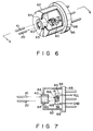
- Figure 6 is a perspective view illustrating a laser amplifier 14 of this invention built in a package.
- Fig. 7 is a sectional view taken along line 6-6 of Fig. 6.
- the laser amplifier 14 is secured onto a heat sink (bed) 60 with, for example, eutectic solder via a submount 59 such as diamond or silicon.
- the rod lens 40 is inserted in an opening 65 made in the cap-like lens holder 62 and then anchored in place with an adhesive member 64 such as solder or silver solder or glass sealer.
- This lens holder 62 is fastened to a stem 68 by, for example, welding 66, to hermetically seal the laser amplifier 14.
- the heat sink 60 is connected to a low-potential power supply GND and the optical waveguide layers 16A and 16B of the chip 14 are connected to a high-potential power supply V cc , which provides an operating potential for the laser amplifier 14.
- optical coupling of the laser amplifier 14 and optical fibers 10 and 20 may be adjusted by fine adjustment of the positions of the optical fibers 10 and 20. That is, optical coupling adjustment of the optical fibers 10 and 20 and the laser amplifier 14 can be made independently of hermetic sealing of the laser amplifier 14, which increases the fabrication productivity of packages.
- Figure 8 is a sectional view illustrating a laser amplifier 14 of the present invention incorporated in a module.
- Fig. 9 is a perspective view enlarging the heat sink 60 and its vicinity.
- an optical fiber holder 80 is fixed onto the lens holder 62 by welding or with an adhesive member 82 such as solder.
- a portion facing the rod lens 40 has an opening 84 made in it.
- a ferrule 86 Inserted in the opening 84 is a ferrule 86, which has two openings 88A and 88B.
- the optical fibers 10 and 20 are inserted in the openings 88A and 88B, respectively.
- fiber strands 10A and 20A extend beyond covering materials 10B and 20B.
- the fiber strands 10A and 20A are fastened in the ferrules 86A and 86B with epoxy resin 90A and 90B.
- the stem 68 on which the heat sink 60 is installed is anchored to an additional stem 94 by welding or with an adhesive member 92 such as solder.
- a cap 98 is secured by welding or with an adhesive member 96 such as solder.
- the cap 98 covers the lens holder 62 and optical fiber holder 80.
- a portion facing the optical fiber holder 80 has two openings 99A and 99B made in it.
- the optical fibers 10 and 20 pass through the openings 99A and 99B, respectively, and appear outside the cap 98.
- another heat sink (bed) 100 is provided on the heat sink 60.
- the laser amplifier 14 of the present invention is secured onto the heat sink 60 with, for example, eutectic solder 102 via the submount 59.
- a P-I-N photodiode (light-receiving element) 50 is fixed with, for example, eutectic solder 104.
- This photodiode 50 has the same function as that of Fig. 5.
- the heat sinks 60 and 100 are connected to a low-potential power supply GND.
- the optical waveguide layers 16A and 16B of the chip 14 are connected to a high-potential power supply V cc1 , and the anode of the photodiode 50 (p-type semiconductor layer) is connected to a high-potential power supply V cc2 , which provides operating potentials for the laser amplifier 14 and photodiode 50.
- V cc1 high-potential power supply
- V cc2 high-potential power supply
- the optical waveguide layers 16A and 16B amplifying light have a structure in which light is reflected at one of the two ends of the resonator, thereby achieving a sufficient amplification gain with a short cavity length L.
- the path along which light is applied to the laser amplifier 14 is different from the path along which light is emitted by the amplifier 14, which requires no beam splitter as shown in Fig. 2. This eliminates signal noise-causing factors. Furthermore, constructing the unit only with high-performance parts whose reliability has been fully verified provides a highly reliable semiconductor laser amplifier.
- the semiconductor laser amplifier 14 is of the buried hetero type, it may be of the double-channel planar buried hetero type or the buried crescent type.
- the present invention may be applicable to the double hetero structure that has a transitional anti-melt-back layer between the active layer 17 and cladding layer 18, or to the distributed feedback laser that has a diffraction grating below the active layer 17.
Abstract
Description
- This invention relates to a semiconductor laser amplifier, and more particularly to a semiconductor laser amplifier used in optical communications to amplify optical signals.
- Since an expensive optical repeater may be replace by only one semiconductor laser amplifier, semiconductor laser amplifiers are expected to significantly reduce the cost of building optical fiber relay networks in the future.
- Figure 1 is a block diagram of a conventional typical semiconductor laser amplifier.
- As shown in Fig. 1, the light propagated along the
optical fiber 10 is supplied via theimage forming lens 12 to theoptical waveguide layer 16 of thesemiconductor laser amplifier 14. Theoptical waveguide layer 16 also serves as an optical active layer, in which light is amplified and leaves theamplifier 14. The amplified light from theamplifier 14 is supplied via theimage forming lens 18 to theoptical fiber 20, returning to the optical fiber relay network. - To achieve a sufficient gain at the
amplifier 14, it is necessary to make the length of theoptical waveguide layer 16 or a cavity length L sufficiently long. For this reason, semiconductor laser amplifiers must have a laser chip length of approximately 400 to 1000 µm, more than twice an ordinary laser chip length of 200 to 300 µm. This leads to a poorer productivity. - Further, in the optical system, it is necessary to connect lenses or fibers to both ends of a chip of the order of 400 to 1000 µm in length, which makes it difficult not only to design and fabricate amplifiers but also to perform important work, such as hermetic sealing, in terms of reliability.
- A semiconductor laser amplifier proposed especially to overcome a poor productivity is shown in Fig. 2.
- As shown in Fig. 2, the light propagated along the
optical fiber 10 is supplied via thebeam splitter 30 to the round-tipoptical fiber 32. The light leaving the round-tipoptical fiber 32 is supplied to the opticalwave guide layer 16 of thesemiconductor laser amplifier 14. The light travels along theoptical waveguide layer 16 increasing its gain until it reaches the end of the resonator. Formed on the end is a high reflection coating film (HR film) 34, which reflects the light. The reflected light then travels backward along theoptical waveguide layer 16 further increasing its gain. The light with the increased gain is supplied again to the round-tipoptical fiber 32, then split at thebeam splitter 30 to go to theoptical fiber 20, and returns to the optical fiber relay network. - By propagating light forward and then backward along the
optical waveguide layer 16 of thesemiconductor laser amplifier 14, it is possible to achieve nearly twice the length of theoptical waveguide layer 16, that is, approximately 2L with respect to the cavity length of L, which provides a small chip with a large gain. - However, because the incoming light and outgoing light are propagated along the same optical waveguide layer, the
beam splitter 30 to sort them must be added in the optical fiber. Presently, it is extremely difficult to completely separate the incoming light from the outgoing light using thebeam splitter 30, which creates problems. For example, leakage of optical components is liable to make signal noises. Some of the light reflected at thebeam splitter 30 can return to theoptical waveguide layer 16, creating a signal noise. There is also a reliability problem: it has not been verified yet that thebeam splitter 30 ensures the sufficiently stable properties against changes in ambient temperatures and aging. - To increase the coupling efficiency of the round-
tip fiber 32, it is necessary to adjust the position with a high accuracy on the submicron order, which makes it difficult to fabricate the optical system. Particularly, in hermetically sealing theamplifier 14 in a package to fabricate a module, the round-tip fiber is soldered or bonded with an adhesive, which often causes misalignment during work, resulting in a poor fabrication yield. - As noted above, in conventional semiconductor laser amplifiers, the length of elements (cavity length) is large, leading to a poor productivity.
- Some semiconductor laser amplifiers are available which have an improved productivity, but the incoming light and outgoing light are still propagated along the same optical fiber, which involves many factors creating signal noises. Use of insufficiently stable parts in terms of a change in ambient temperature and aging impairs the reliability. In addition, use of a round-tip fiber necessitates submicron adjustment in fabricating the module, making the work difficult.
- Accordingly, the object of the present invention is to provide a highly reliable semiconductor laser amplifier with a high productivity.
- In this invention, an optical waveguide layer, which is formed in a semiconductor substrate of a first conductivity type and contains a semiconductor layer of a second conductivity type, is arranged so as to form a V in a plane, which virtually makes the length of the optical waveguide layer twice the cavity length and differs the light incoming path from the light outgoing path.
- With this semiconductor laser amplifier, since the length of the optical waveguide layer is virtually twice the cavity length, it is possible to shorten the cavity length without reducing the gain. Consequently, the number of laser amplifiers per wafer increases, improving the productivity of laser amplifiers.
- Difference of the light incoming path from the light outgoing path decreases factors of creating signal noises such as light reflection, which improves the performance of the laser amplifier. Further, constructing the laser amplifier only with parts whose stability has been fully verified improves the reliability.
- This invention can be more fully understood from the following detailed description when taken in conjunction with the accompanying drawings, in which:
- Fig. 1 is a schematic diagram of a conventional laser amplifier system;
- Fig. 2 is a schematic diagram of another conventional laser amplifier system;
- Fig. 3 is a schematic diagram for a semiconductor laser amplifier system according to a first embodiment of the present invention;
- Fig. 4 is a perspective view, partially in cross-section, of a semiconductor laser amplifier according to the present invention;
- Fig. 5 is a schematic diagram of a semiconductor laser amplifier system according to a second embodiment of the present invention;
- Fig. 6 is a perspective view illustrating a semiconductor laser amplifier of the present invention built in a package;
- Fig. 7 is a sectional view taken along line 6-6;
- Fig. 8 is a sectional view illustrating a laser amplifier of this invention incorporated in a module;
- Fig. 9 is a perspective view enlarging the heat sink and its vicinity in Fig. 8; and
- Fig. 10 is a sectional view illustrating a laser amplifier of this invention incorporated in a another module.
- Referring to the accompanying drawings, embodiments of the present invention will be explained. Like parts are shown by corresponding reference characters throughout several views, and redundant explanations will be avoided.
- Figure 3 is a schematic diagram of a semiconductor laser amplifier system according to a first embodiment of the present invention.
- As shown in Fig. 3, the
light 11A propagated along anoptical fiber 10 passes through arod lens 40 and enters anoptical waveguide layer 16A at itsincident end 14A of alaser amplifier 14. On theincident end 14A, for example, an anti-reflective film (AR film) 13 is placed. Thelight 11A goes into theoptical waveguide layer 16A via theanti-reflective film 13. Theoptical waveguide layer 16A also serves as an optical active layer, in which the incident light is amplified. A high reflection coating film (HR film) 15 is placed on thereflective end 14B of thelaser amplifier 14. The light traveling along theoptical waveguide layer 16A increasing its gain is reflected at the highreflection coating film 15 and advances toward theoptical waveguide layer 16B. To reflect light, a cleavage surface may be used as thereflective end 14B instead of thehigh reflection film 15. Theoptical waveguide layer 16B also serves as an optical active layer that amplifies light as does theoptical waveguide layer 16A. The light traveling along theoptical waveguide layer 16B increasing its gain reaches theincident end 14A and leaves thelaser amplifier 14 to the outside via theanti-reflective film 13. Thisoutgoing light 11B enters theoptical fiber 20 via therod lens 40. Use of therod lens 40 makes it possible to spatially differ the incoming light from the outgoing light, along the paths from theoptical waveguide layers optical fibers rod lens 40 is required. With a single rod lens, simple adjustment of the incident angle of light entering or leaving thefibers optical fiber 10 to thelaser amplifier 14 and the focal point of light advancing from theamplifier 14 to thefiber 20. - Figure 4 is a perspective view, partially in cross-section, of a semiconductor laser amplifier according to the present invention. The semiconductor laser amplifier is, for example, of the same type as that of the
amplifier 14 in the system of Fig. 3. In this embodiment, an InGaAsP-based buried hetero semiconductor laser will be explained as an example. - As shown in Fig. 4, on an n-
type InP substrate 60, theoptical waveguide layers active layer 62, a p-typeInP cladding layer 64, and a p-type InGaAsPohmic contact layer 66. Theoptical waveguide layers active layer 62, p-typeInP cladding layer 64, and p-type InGaAsPohmic contact layer 66, a p-type InP buriedlayer 68, and an n-type InP buriedlayer 70 are formed to block current and light.Electrodes laser amplifier 14, respectively. With supply of current from theseelectrodes optical waveguide layers incident end 14A of thelaser amplifier 14, ananti-reflective film 13 is formed, while on its reflective end, a highreflection coating film 15 is formed. The reflectivity of theanti-reflective film 13 is set to a value on the order of 10⁻³ or less at the end of theoptical waveguide layers reflection coating film 15 is set to a value in the range of 0.3 to 1.0. Adjusting the product of these reflectivities to the order of 10⁻⁴ or less suppresses laser oscillation, which allows thelaser amplifier 14 to function as the progressive-wave type. - Figure 5 is a schematic diagram of a semiconductor laser amplifier system according to a second embodiment of the present invention.
- When the reflectivity of the high
reflection coating film 15 is less than 1.0, self-adjustment of optical amplification is possible by as shown in Fig. 5, installing a light-receiving element for automatic gain adjustment, such as aphotodiode 50, on the side of thereflective end 14B, and supplying the light-caused current at thephotodiode 50 to anautomatic power controller 52, which controls current supply to thelaser amplifier 14. - Semiconductor laser amplifiers of the above-mentioned structure are manufactured in almost the same way as the manufacturing method of ordinary buried hetero laser elements. For example, on the n-
type InP substrate 60, theactive layer 62, p-typeInP cladding layer 64, and p-type InGaAsPohmic contact layer 66 are formed sequentially. Then, these layers are selectively etched by, for example, photoetching so as to form theoptical waveguide layers active layer 62, and when viewed from the top, shape like a V. After this, the p-type InP buriedlayer 68 and n-type InP buriedlayer 70 are grown in sequence along the sides of the mesa stripe to form thelaser amplifier 14. Next, a metal coating to formelectrodes laser amplifier 14. After this, the wafer is cloven intoindividual laser amplifiers 14. After cleavage, on bothends laser amplifier 14, theanti-reflective film 13 and highreflection coating film 15 and others are formed as required. - Figure 6 is a perspective view illustrating a
laser amplifier 14 of this invention built in a package. Fig. 7 is a sectional view taken along line 6-6 of Fig. 6. - As shown in Figs. 6 and 7, the
laser amplifier 14 is secured onto a heat sink (bed) 60 with, for example, eutectic solder via asubmount 59 such as diamond or silicon. Therod lens 40 is inserted in anopening 65 made in the cap-like lens holder 62 and then anchored in place with anadhesive member 64 such as solder or silver solder or glass sealer. Thislens holder 62 is fastened to astem 68 by, for example, welding 66, to hermetically seal thelaser amplifier 14. As shown in Fig. 7, theheat sink 60 is connected to a low-potential power supply GND and theoptical waveguide layers chip 14 are connected to a high-potential power supply Vcc, which provides an operating potential for thelaser amplifier 14. - With this package, optical coupling of the
laser amplifier 14 andoptical fibers optical fibers optical fibers laser amplifier 14 can be made independently of hermetic sealing of thelaser amplifier 14, which increases the fabrication productivity of packages. - Figure 8 is a sectional view illustrating a
laser amplifier 14 of the present invention incorporated in a module. Fig. 9 is a perspective view enlarging theheat sink 60 and its vicinity. - As shown in Fig. 8, an
optical fiber holder 80 is fixed onto thelens holder 62 by welding or with anadhesive member 82 such as solder. In theoptical fiber holder 80, a portion facing therod lens 40 has an opening 84 made in it. Inserted in the opening 84 is a ferrule 86, which has twoopenings optical fibers openings optical fibers lens 40,fiber strands materials fiber strands epoxy resin stem 68 on which theheat sink 60 is installed is anchored to anadditional stem 94 by welding or with anadhesive member 92 such as solder. Onto thestem 94, acap 98 is secured by welding or with anadhesive member 96 such as solder. Thecap 98 covers thelens holder 62 andoptical fiber holder 80. In thecap 98, a portion facing theoptical fiber holder 80 has twoopenings optical fibers openings cap 98. - In the module, as shown in Fig. 9, on the
heat sink 60, another heat sink (bed) 100 is provided. Thelaser amplifier 14 of the present invention is secured onto theheat sink 60 with, for example, eutectic solder 102 via thesubmount 59. On theadditional heat sink 100, a P-I-N photodiode (light-receiving element) 50 is fixed with, for example,eutectic solder 104. Thisphotodiode 50 has the same function as that of Fig. 5. The heat sinks 60 and 100 are connected to a low-potential power supply GND. Theoptical waveguide layers chip 14 are connected to a high-potential power supply Vcc1, and the anode of the photodiode 50 (p-type semiconductor layer) is connected to a high-potential power supply Vcc2, which provides operating potentials for thelaser amplifier 14 andphotodiode 50. Further, as shown in Fig. 10, by building the module of Fig. 9 in a rectangular package such as a dual-in-line (DIL) package or a butterfly package, it is possible to facilitate circuit board mounting. - As described so far, with the semiconductor laser amplifier according to the present invention, the
optical waveguide layers laser amplifier 14 smaller, improving the productivity oflaser amplifiers 14. Since both receiving and transmitting of light is done at the remaining end of thelaser amplifier 14, there is no need to develop a special package at all, and packages similar to conventional ones for semiconductor lasers may be used. Further, optical coupling adjustment can be made at only one place, facilitating optical coupling adjustment compared with conventional equivalents as shown in Fig. 1 where lenses are placed on both sides of the resonator. - The path along which light is applied to the
laser amplifier 14 is different from the path along which light is emitted by theamplifier 14, which requires no beam splitter as shown in Fig. 2. This eliminates signal noise-causing factors. Furthermore, constructing the unit only with high-performance parts whose reliability has been fully verified provides a highly reliable semiconductor laser amplifier. - This invention may be practiced or embodied in still other ways without departing from the spirit or essential character thereof. For example, while in the embodiments, the
semiconductor laser amplifier 14 is of the buried hetero type, it may be of the double-channel planar buried hetero type or the buried crescent type. In addition, the present invention may be applicable to the double hetero structure that has a transitional anti-melt-back layer between the active layer 17 andcladding layer 18, or to the distributed feedback laser that has a diffraction grating below the active layer 17.
Claims (10)
- A semiconductor laser amplifier having a semiconductor substrate (60 and 70) of a first conductivity type having a first end (14A) and a second end (14B), characterized by comprising:
a first optical waveguide layer (16A) that contains a semiconductor layer (64) of a second conductivity type, and that is formed in said substrate (60 and 70) so that one end of the waveguide layer may be in contact with said first end (14A) and the other end in contact with said second end (14B);
reflecting means (15) that is formed on the second end (14B) of said substrate and that reflects the light propagated along said first optical waveguide layer (16A); and
a second optical waveguide layer (16B) that contains a semiconductor layer (64) of the second conductivity type, and that is formed in said substrate (60 and 70) so that one end of the waveguide layer may be in contact with said first end (14A) and the other end in contact with the other end of said first optical waveguide layer (16A). - The semiconductor laser amplifier according to claim 1, characterized in that said first optical waveguide layer (16A) receives light (11A) from outside said substrate (60 and 70) via said first end (14A) and amplifies it, and said second optical waveguide layer (16B) receives the reflected light from said reflecting means (15), amplifies it, and emits the light (11B) outward from said substrate (60 and 70) via said first end (14A).
- The semiconductor laser amplifier according to claim 1 or 2, characterized in that said reflecting means (15) is a reflective film (15) formed on said second end (14B).
- The semiconductor laser amplifier according to claim 1 or 2, characterized in that said reflecting means (15) is a cleavage surface serving as said second end (14B) formed by cleaving said substrate (60 and 70).
- The semiconductor laser amplifier according to claim 2, characterized in that the reflectivity R1 of said first end (14A) is:

the reflectivity R2 of said reflecting means formed on said second end (14B) is:

and the product of said reflectivities R1 and R2 is:

- The semiconductor laser amplifier according to claim 1 or 2, characterized by further comprising an anti-reflective film (13) formed on said first end (14A).
- A semiconductor laser amplifier module, characterized by comprising:
a semiconductor laser amplifier that comprises a semiconductor substrate (60 and 70) of a first conductivity type having a first end (14A) and a second end (14B), a first optical waveguide layer (16A) that contains a semiconductor layer (64) of a second conductivity type and that is formed in said substrate (60 and 70) so that one end of the wave guide layer may be in contact with said first end (14A) and the other end in contact with said second end (14B), reflecting means (15) that is formed on the second end (14B) of said substrate (60 and 70) and that reflects the light propagated along said first optical waveguide layer (16A), and a second optical waveguide layer (16B) that contains a semiconductor layer (64) of the second conductivity type and that is formed in said substrate (60 and 70) so that one of the waveguide layer may be in contact with said first end (14A) and the other end in contact with the other end of said optical waveguide layer (16A);
a submount (59) and a bed (60) on which said semiconductor laser amplifier (14) is installed;
a stem (68) on which said bed (60) is installed;
a first holder (62) that is installed to said stem (68) and has a support (65) at a portion facing the first end (14A) of said semiconductor laser amplifier (14);
a lens (40) held in place by the support (65) of said first holder (62);
a second holder (80) that is installed to said first holder (62) and has a support (84) at a portion facing said lens (40); and
a first and second optical fibers (10 and 20) held in place by the support (84) of said second holder (80). - The semiconductor laser amplifier module according to claim 7, characterized by further comprising:
an additional stem (94) on which said stem (68) is in stalled;
a cap (98) that is installed on said additional stem (94) and that covers said first holder (62) and second holder (80); and
a first and second openings (99A and 99B) made in said cap (98), in which said first and second optical fibers (10 and 20) are inserted, respectively. - The semiconductor laser amplifier module according to claim 7 or 8, characterized by further comprising:
an additional bed (100) formed at a portion of said bed (60) facing the second end (14B) of said semiconductor laser amplifier (14); and
a photodiode (50) installed on said additional bed (100). - The semiconductor laser amplifier module according to claim 7, 8, or 9, characterized in that said lens (40) is a rod lens (40).
Applications Claiming Priority (2)
| Application Number | Priority Date | Filing Date | Title |
|---|---|---|---|
| JP257110/90 | 1990-09-28 | ||
| JP2257110A JP2539089B2 (en) | 1990-09-28 | 1990-09-28 | Semiconductor laser amplifier and semiconductor laser amplifier |
Publications (3)
| Publication Number | Publication Date |
|---|---|
| EP0477842A2 true EP0477842A2 (en) | 1992-04-01 |
| EP0477842A3 EP0477842A3 (en) | 1992-06-03 |
| EP0477842B1 EP0477842B1 (en) | 1995-12-20 |
Family
ID=17301874
Family Applications (1)
| Application Number | Title | Priority Date | Filing Date |
|---|---|---|---|
| EP91116210A Expired - Lifetime EP0477842B1 (en) | 1990-09-28 | 1991-09-24 | Semiconducteur laser amplifier |
Country Status (5)
| Country | Link |
|---|---|
| US (1) | US5229879A (en) |
| EP (1) | EP0477842B1 (en) |
| JP (1) | JP2539089B2 (en) |
| KR (2) | KR950006317B1 (en) |
| DE (1) | DE69115622T2 (en) |
Families Citing this family (13)
| Publication number | Priority date | Publication date | Assignee | Title |
|---|---|---|---|---|
| JP2891856B2 (en) * | 1993-10-14 | 1999-05-17 | 日本電気株式会社 | Optical path conversion circuit |
| US5646674A (en) * | 1994-04-29 | 1997-07-08 | Eastman Kodak Company | Optical print head with flexure mounted optical device |
| US5657148A (en) * | 1996-05-07 | 1997-08-12 | Lucent Technologies Inc. | Apparatus and method for a single-port modulator having amplification |
| GB2344692A (en) * | 1998-12-11 | 2000-06-14 | Bookham Technology Ltd | Optical amplifier |
| EP1043818B1 (en) * | 1999-04-09 | 2011-07-20 | Mitsui Chemicals, Inc. | Semiconductor laser device, semiconductor laser module, rare-earth-element-doped optical fiber amplifier and fiber laser |
| US6870667B2 (en) * | 2001-11-27 | 2005-03-22 | Sumitomo Electric Industries, Ltd. | Optical amplifier |
| KR100584400B1 (en) * | 2005-01-06 | 2006-05-26 | 삼성전자주식회사 | Gain-flattened broadband light source |
| JP2006201313A (en) * | 2005-01-18 | 2006-08-03 | Fuji Xerox Co Ltd | Optical transmission apparatus and optical module |
| US7171066B1 (en) * | 2005-09-07 | 2007-01-30 | Fuji Xerox Co., Ltd. | Optical module and optical transmission device |
| US7738167B2 (en) * | 2005-12-09 | 2010-06-15 | Electronics And Telecommunications Research Institute | Reflective semiconductor optical amplifier (RSOA), RSOA module having the same, and passive optical network using the same |
| KR100987793B1 (en) * | 2008-10-10 | 2010-10-13 | 한국전자통신연구원 | Reflective semiconductor optical amplifier and optical signal treating method using the same |
| JP5055306B2 (en) * | 2009-01-27 | 2012-10-24 | アンリツ株式会社 | Semiconductor optical amplification system |
| JP2018006619A (en) * | 2016-07-05 | 2018-01-11 | 富士通株式会社 | Optical element and light generation device |
Citations (7)
| Publication number | Priority date | Publication date | Assignee | Title |
|---|---|---|---|---|
| US4152713A (en) * | 1977-12-05 | 1979-05-01 | Bell Telephone Laboratories, Incorporated | Unidirectional optical device and regenerator |
| GB2033648A (en) * | 1978-10-19 | 1980-05-21 | Kokusai Denshin Denwa Co Ltd | Semi-conductor light amplifier |
| JPS5728392A (en) * | 1980-07-29 | 1982-02-16 | Fujitsu Ltd | Optical semiconductor device |
| JPS60136387A (en) * | 1983-12-26 | 1985-07-19 | Hitachi Ltd | Light element module |
| JPS62170918A (en) * | 1986-01-24 | 1987-07-28 | Nec Corp | Semiconductor laser module |
| EP0245085A1 (en) * | 1986-05-08 | 1987-11-11 | BRITISH TELECOMMUNICATIONS public limited company | Optical amplifiers |
| JPS63221692A (en) * | 1987-03-10 | 1988-09-14 | Oki Electric Ind Co Ltd | Semiconductor light amplifier |
Family Cites Families (5)
| Publication number | Priority date | Publication date | Assignee | Title |
|---|---|---|---|---|
| EP0288267B1 (en) * | 1987-04-21 | 1993-10-06 | Nec Corporation | An optical semiconductor device |
| JPS63316812A (en) * | 1987-06-19 | 1988-12-26 | Toshiba Corp | Photosemiconductor device |
| JPH01293584A (en) * | 1988-05-20 | 1989-11-27 | Nec Corp | Light-amplifying device |
| JP2941298B2 (en) * | 1989-03-07 | 1999-08-25 | 株式会社東芝 | Optical element module |
| US5019787A (en) * | 1989-10-30 | 1991-05-28 | David Sarnoff Research Center, Inc. | Optical amplifier |
-
1990
- 1990-09-28 JP JP2257110A patent/JP2539089B2/en not_active Expired - Fee Related
-
1991
- 1991-09-24 DE DE69115622T patent/DE69115622T2/en not_active Expired - Fee Related
- 1991-09-24 EP EP91116210A patent/EP0477842B1/en not_active Expired - Lifetime
- 1991-09-26 US US07/765,900 patent/US5229879A/en not_active Expired - Lifetime
- 1991-09-28 KR KR1019910016969A patent/KR950006317B1/en active
- 1991-09-28 KR KR1019910016969A patent/KR920007279A/en not_active IP Right Cessation
Patent Citations (7)
| Publication number | Priority date | Publication date | Assignee | Title |
|---|---|---|---|---|
| US4152713A (en) * | 1977-12-05 | 1979-05-01 | Bell Telephone Laboratories, Incorporated | Unidirectional optical device and regenerator |
| GB2033648A (en) * | 1978-10-19 | 1980-05-21 | Kokusai Denshin Denwa Co Ltd | Semi-conductor light amplifier |
| JPS5728392A (en) * | 1980-07-29 | 1982-02-16 | Fujitsu Ltd | Optical semiconductor device |
| JPS60136387A (en) * | 1983-12-26 | 1985-07-19 | Hitachi Ltd | Light element module |
| JPS62170918A (en) * | 1986-01-24 | 1987-07-28 | Nec Corp | Semiconductor laser module |
| EP0245085A1 (en) * | 1986-05-08 | 1987-11-11 | BRITISH TELECOMMUNICATIONS public limited company | Optical amplifiers |
| JPS63221692A (en) * | 1987-03-10 | 1988-09-14 | Oki Electric Ind Co Ltd | Semiconductor light amplifier |
Non-Patent Citations (4)
| Title |
|---|
| PATENT ABSTRACTS OF JAPAN vol. 12, no. 12 (P-655)14 January 1988 & JP-A-62 170 918 ( NEC ) * |
| PATENT ABSTRACTS OF JAPAN vol. 13, no. 16 (E-703)(3364) 13 January 1989 & JP-A-63 221 692 ( OKI ELECTRIC IND ) * |
| PATENT ABSTRACTS OF JAPAN vol. 6, no. 95 (E-110)3 June 1982 & JP-A-57 028 392 * |
| PATENT ABSTRACTS OF JAPAN vol. 9, no. 298 (E-361)26 November 1985 & JP-A-60 136 387 ( HITACHI SEISAKUSHO KK ) * |
Also Published As
| Publication number | Publication date |
|---|---|
| KR920007279A (en) | 1992-04-28 |
| EP0477842A3 (en) | 1992-06-03 |
| DE69115622D1 (en) | 1996-02-01 |
| EP0477842B1 (en) | 1995-12-20 |
| KR950006317B1 (en) | 1995-06-13 |
| DE69115622T2 (en) | 1996-05-30 |
| JPH04136824A (en) | 1992-05-11 |
| US5229879A (en) | 1993-07-20 |
| JP2539089B2 (en) | 1996-10-02 |
Similar Documents
| Publication | Publication Date | Title |
|---|---|---|
| US5566265A (en) | Transmission and reception module for a bidirectional, optical message and signal transmission | |
| US6314117B1 (en) | Laser diode package | |
| US5875205A (en) | Optoelectronic component and method for the manufacture thereof | |
| US20030099273A1 (en) | Method and apparatus for coupling a surface-emitting laser to an external device | |
| US20060239612A1 (en) | Flip-chip devices formed on photonic integrated circuit chips | |
| EP0477842B1 (en) | Semiconducteur laser amplifier | |
| JP2930213B2 (en) | Semiconductor laser device | |
| JP4639578B2 (en) | Semiconductor laser module and manufacturing method thereof | |
| JP2628774B2 (en) | Semiconductor laser module with built-in optical isolator | |
| EP0948104B1 (en) | Semiconductor laser module and method of manufacturing the same | |
| US6212212B1 (en) | Optical module | |
| KR100734874B1 (en) | Bi-directional optical module | |
| JP2003107295A (en) | Optical transmission module | |
| EP0623980A2 (en) | Semiconductor laser with transverse emission, and coupling thereof to an optical waveguide | |
| US7018110B2 (en) | Optical module | |
| EP1353421B1 (en) | Optical module with a monitor photo diode | |
| JP3042453B2 (en) | Light receiving module | |
| JPH07199006A (en) | Optical subassembly and optical module | |
| US20070147747A1 (en) | Optical module and optical transmission system using the same | |
| US5675597A (en) | Semiconductor laser device | |
| US20040141699A1 (en) | Optical module | |
| JP3032376B2 (en) | Semiconductor laser device | |
| JP3508396B2 (en) | Method of manufacturing bar code reading composite optical device | |
| JPH04275483A (en) | Semiconductor laser light amplifier | |
| JPH0983085A (en) | Semiconductor laser and assembling method therefor |
Legal Events
| Date | Code | Title | Description |
|---|---|---|---|
| PUAI | Public reference made under article 153(3) epc to a published international application that has entered the european phase |
Free format text: ORIGINAL CODE: 0009012 |
|
| 17P | Request for examination filed |
Effective date: 19910924 |
|
| AK | Designated contracting states |
Kind code of ref document: A2 Designated state(s): DE FR GB |
|
| PUAL | Search report despatched |
Free format text: ORIGINAL CODE: 0009013 |
|
| AK | Designated contracting states |
Kind code of ref document: A3 Designated state(s): DE FR GB |
|
| 17Q | First examination report despatched |
Effective date: 19931006 |
|
| GRAA | (expected) grant |
Free format text: ORIGINAL CODE: 0009210 |
|
| AK | Designated contracting states |
Kind code of ref document: B1 Designated state(s): DE FR GB |
|
| REF | Corresponds to: |
Ref document number: 69115622 Country of ref document: DE Date of ref document: 19960201 |
|
| ET | Fr: translation filed | ||
| PLBE | No opposition filed within time limit |
Free format text: ORIGINAL CODE: 0009261 |
|
| STAA | Information on the status of an ep patent application or granted ep patent |
Free format text: STATUS: NO OPPOSITION FILED WITHIN TIME LIMIT |
|
| 26N | No opposition filed | ||
| PGFP | Annual fee paid to national office [announced via postgrant information from national office to epo] |
Ref country code: FR Payment date: 19970909 Year of fee payment: 7 |
|
| PGFP | Annual fee paid to national office [announced via postgrant information from national office to epo] |
Ref country code: GB Payment date: 19970915 Year of fee payment: 7 |
|
| PG25 | Lapsed in a contracting state [announced via postgrant information from national office to epo] |
Ref country code: GB Free format text: LAPSE BECAUSE OF NON-PAYMENT OF DUE FEES Effective date: 19980924 |
|
| GBPC | Gb: european patent ceased through non-payment of renewal fee |
Effective date: 19980924 |
|
| PG25 | Lapsed in a contracting state [announced via postgrant information from national office to epo] |
Ref country code: FR Free format text: LAPSE BECAUSE OF NON-PAYMENT OF DUE FEES Effective date: 19990531 |
|
| REG | Reference to a national code |
Ref country code: FR Ref legal event code: ST |
|
| PGFP | Annual fee paid to national office [announced via postgrant information from national office to epo] |
Ref country code: DE Payment date: 20050922 Year of fee payment: 15 |
|
| PG25 | Lapsed in a contracting state [announced via postgrant information from national office to epo] |
Ref country code: DE Free format text: LAPSE BECAUSE OF NON-PAYMENT OF DUE FEES Effective date: 20070403 |