EP0476883B2 - Electrical connector assembly - Google Patents
Electrical connector assembly Download PDFInfo
- Publication number
- EP0476883B2 EP0476883B2 EP91308042A EP91308042A EP0476883B2 EP 0476883 B2 EP0476883 B2 EP 0476883B2 EP 91308042 A EP91308042 A EP 91308042A EP 91308042 A EP91308042 A EP 91308042A EP 0476883 B2 EP0476883 B2 EP 0476883B2
- Authority
- EP
- European Patent Office
- Prior art keywords
- mating
- terminal
- extending
- members
- terminal members
- Prior art date
- Legal status (The legal status is an assumption and is not a legal conclusion. Google has not performed a legal analysis and makes no representation as to the accuracy of the status listed.)
- Expired - Lifetime
Links
Images


Classifications
-
- H—ELECTRICITY
- H01—ELECTRIC ELEMENTS
- H01R—ELECTRICALLY-CONDUCTIVE CONNECTIONS; STRUCTURAL ASSOCIATIONS OF A PLURALITY OF MUTUALLY-INSULATED ELECTRICAL CONNECTING ELEMENTS; COUPLING DEVICES; CURRENT COLLECTORS
- H01R13/00—Details of coupling devices of the kinds covered by groups H01R12/70 or H01R24/00 - H01R33/00
- H01R13/648—Protective earth or shield arrangements on coupling devices, e.g. anti-static shielding
- H01R13/658—High frequency shielding arrangements, e.g. against EMI [Electro-Magnetic Interference] or EMP [Electro-Magnetic Pulse]
- H01R13/6581—Shield structure
-
- H—ELECTRICITY
- H01—ELECTRIC ELEMENTS
- H01R—ELECTRICALLY-CONDUCTIVE CONNECTIONS; STRUCTURAL ASSOCIATIONS OF A PLURALITY OF MUTUALLY-INSULATED ELECTRICAL CONNECTING ELEMENTS; COUPLING DEVICES; CURRENT COLLECTORS
- H01R12/00—Structural associations of a plurality of mutually-insulated electrical connecting elements, specially adapted for printed circuits, e.g. printed circuit boards [PCB], flat or ribbon cables, or like generally planar structures, e.g. terminal strips, terminal blocks; Coupling devices specially adapted for printed circuits, flat or ribbon cables, or like generally planar structures; Terminals specially adapted for contact with, or insertion into, printed circuits, flat or ribbon cables, or like generally planar structures
- H01R12/70—Coupling devices
- H01R12/71—Coupling devices for rigid printing circuits or like structures
- H01R12/72—Coupling devices for rigid printing circuits or like structures coupling with the edge of the rigid printed circuits or like structures
- H01R12/73—Coupling devices for rigid printing circuits or like structures coupling with the edge of the rigid printed circuits or like structures connecting to other rigid printed circuits or like structures
- H01R12/735—Printed circuits including an angle between each other
- H01R12/737—Printed circuits being substantially perpendicular to each other
-
- H—ELECTRICITY
- H01—ELECTRIC ELEMENTS
- H01R—ELECTRICALLY-CONDUCTIVE CONNECTIONS; STRUCTURAL ASSOCIATIONS OF A PLURALITY OF MUTUALLY-INSULATED ELECTRICAL CONNECTING ELEMENTS; COUPLING DEVICES; CURRENT COLLECTORS
- H01R12/00—Structural associations of a plurality of mutually-insulated electrical connecting elements, specially adapted for printed circuits, e.g. printed circuit boards [PCB], flat or ribbon cables, or like generally planar structures, e.g. terminal strips, terminal blocks; Coupling devices specially adapted for printed circuits, flat or ribbon cables, or like generally planar structures; Terminals specially adapted for contact with, or insertion into, printed circuits, flat or ribbon cables, or like generally planar structures
- H01R12/70—Coupling devices
- H01R12/71—Coupling devices for rigid printing circuits or like structures
- H01R12/712—Coupling devices for rigid printing circuits or like structures co-operating with the surface of the printed circuit or with a coupling device exclusively provided on the surface of the printed circuit
- H01R12/716—Coupling device provided on the PCB
-
- H—ELECTRICITY
- H01—ELECTRIC ELEMENTS
- H01R—ELECTRICALLY-CONDUCTIVE CONNECTIONS; STRUCTURAL ASSOCIATIONS OF A PLURALITY OF MUTUALLY-INSULATED ELECTRICAL CONNECTING ELEMENTS; COUPLING DEVICES; CURRENT COLLECTORS
- H01R12/00—Structural associations of a plurality of mutually-insulated electrical connecting elements, specially adapted for printed circuits, e.g. printed circuit boards [PCB], flat or ribbon cables, or like generally planar structures, e.g. terminal strips, terminal blocks; Coupling devices specially adapted for printed circuits, flat or ribbon cables, or like generally planar structures; Terminals specially adapted for contact with, or insertion into, printed circuits, flat or ribbon cables, or like generally planar structures
- H01R12/70—Coupling devices
- H01R12/71—Coupling devices for rigid printing circuits or like structures
- H01R12/72—Coupling devices for rigid printing circuits or like structures coupling with the edge of the rigid printed circuits or like structures
- H01R12/722—Coupling devices for rigid printing circuits or like structures coupling with the edge of the rigid printed circuits or like structures coupling devices mounted on the edge of the printed circuits
- H01R12/724—Coupling devices for rigid printing circuits or like structures coupling with the edge of the rigid printed circuits or like structures coupling devices mounted on the edge of the printed circuits containing contact members forming a right angle
-
- H—ELECTRICITY
- H01—ELECTRIC ELEMENTS
- H01R—ELECTRICALLY-CONDUCTIVE CONNECTIONS; STRUCTURAL ASSOCIATIONS OF A PLURALITY OF MUTUALLY-INSULATED ELECTRICAL CONNECTING ELEMENTS; COUPLING DEVICES; CURRENT COLLECTORS
- H01R13/00—Details of coupling devices of the kinds covered by groups H01R12/70 or H01R24/00 - H01R33/00
- H01R13/648—Protective earth or shield arrangements on coupling devices, e.g. anti-static shielding
- H01R13/658—High frequency shielding arrangements, e.g. against EMI [Electro-Magnetic Interference] or EMP [Electro-Magnetic Pulse]
Definitions
- This invention relates to an electrical connector assembly for electrically interconnecting corresponding circuits between two circuit boards.
- Board to board connectors are used to interconnect circuitry on a plurality of daughter boards to a mother board or backplane. These boards may be mounted in a vertical or horizontal relationship depending upon the configuration of the mating connector members.
- U.S. Patent 4,867,690 discloses an electrical connector system comprising a pin header having a plurality of rows of terminal members extending parallel to the sidewalls. The outermost rows of terminals adjacent the sidewalls are adapted to provide ground reference paths while the remaining rows of terminals are adapted to be mated to a receptacle member.
- U.S. Patent 4,655,518 discloses an electrical connector and a two-piece connector assembly providing grounding contacts along the dielectric sidewalls of the respective connectors.
- the terminal members of the pin header are positioned in recesses along the inside surfaces of the sidewall with the contact portion being a convex shape single resilient beam facing inwardly toward the pin terminals positioned between the sidewalls.
- ground contacts are placed along the outside surfaces of the sidewall so that they will slidably engage resilient beams in the pin header when the connectors are mated.
- connector assemblies used within the system include means for facilitating interconnection of module shields to ground planes within the mother board or backplane.
- shield pin header shielded receptacle
- shield connector assembly shielded connector assembly
- the mating members of grounded or shielded connector assembly also be matable with respective existing complementary non-grounded or shielded members to provide a cost effective manner of upgrading existing electronic systems such as computers and instrumentation.
- the present invention is directed to an electrical connector system that eliminates the problems and disadvantages of the prior art and consists in an electrical connector according to claim 1 and in an electrical connector assembly according to claim 3.
- FR 2590415 discloses an electrical connector and an electrical connector assembly according to the preambles of claims 1 and 3.
- the invention enables an improvement in the electrical performance of the connector by providing additional low inductance and low resistance paths for ground current to flow through the electrical connector assembly to a circuit board. Moreover, it can provide a shielded connector system that is also compatible with existing unshielded connectors.
- means may be provided for shunting or switching adjacent contact terminals to provide electrical continuity upon removal of a board from a system, thereby eliminating the need to use additional components to provide the same function.
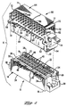
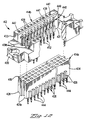
- the connector assembly 10 of the present invention comprises a receptacle member 12 and a pin header 60.
- the board to board connector assembly 10 is shown in a configuration suitable for mounting daughter cards perpendicular to the mother board or backplane. It is to be understood that the pin header member can be modified for positioning the daughter cards in parallel with the mother board.
- Receptacle member 12 includes a housing member 14 having a mating face 16 and a mounting face 18. Housing 14 has a transverse body section 20 extending along the mounting face 18 as best seen in Figure 4, an inner body portion 22 and opposed outer side walls 34 extending from mounting face 18 to mating face 16 and defining elongate cavities 36 between the inner body portion 22 and respective outer side walls 34.
- Inner body portion 22 includes opposed side walls 24, end walls 28 having mounting flanges 30 extending outwardly therefrom, and a plurality of terminal-receiving passageways 32 extending from the mounting face 18 to the mating face 16.
- a plurality of first contact terminal members 40 are disposed in respective passageways 32, as shown in Figures 2 and 3. For purposes of illustration, first terminal members 40 have been eliminated in Figures 1 and 4.
- First terminal members 40 include a first contact section 42 for mating with complementary terminal members 78 of pin header 60 and a second contact section 44 extending below the mounting face 18 for engagement with corresponding apertures 104 of the circuit board 102.
- elongate cavities 36 are defined along thin sides by the inner surface of outer side walls 34 and the corresponding outer surfaces of body side walls 24 and the respective portions of transverse wall 20 extending therebetween forms cavity base 21.
- Cavity base 21 includes a plurality of apertures 38 extending therethrough.
- Receptacle 12 further includes a plurality of second contact terminal members 46 disposed in terminal-receiving apertures 38 of transverse wall 20 and having first contact sections 48 extending into elongate cavities 36 and a second contact section 52 extending outwardly from mounting face 18 for engagement with apertures 106 of mother board or backplane 102.
- first terminal section 48 of respective second contact terminals 46 include cantilevered beam portions having an inwardly directed arcuate section 49 and a contact surface 50 intermediate arcuate section 49 and second contact section 52.
- Corresponding contact surfaces 50 of second terminal members 46 are adapted to mate with corresponding ground bus means 84,90 of the complementary mating connector 60 as shown in Figure 3.
- FIGS 4 and 5 illustrate an alternative receptacle member embodiment 120, which includes at least one shunt terminal member 54 to provide an internal "switching effect.” Since the basic structure of receptacle member 120 is essentially the same as that of receptacle member 12, the same reference numerals have been used for the identical parts.
- Receptacle member 120 includes a housing member 140 having a transverse body section 20 extending along the mounting face 18 as best seen in Figure 4, an inner body portion 122 and opposed outer side walls 34 extending upward from the mounting face 18 and defining elongate cavities 36 between the inner body portion 122 and respective outer side walls 34.
- Inner body portion 122 includes opposed side walls 124, end walls 28 having mounting flanges 30 extending outwardly therefrom.
- the outside surfaces of side walls 124 of inner body portion 122 further include projections 126 extending into respective cavities 36 at selected locations therealong.
- Projections 126 include slots 127 for receiving a shunt terminal member 54 therebetween.
- Shunt terminal member 54 includes an outwardly extending portion 56 and ends 58, the ends 58 being received in projection slots 127 and extending between two adjacent second terminal members 46.
- shunt terminal member 54 electrically interconnects two adjacent second terminal members 46 within a respective cavity 36, when the receptacle member 120 is not mated to a complementary connector.
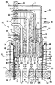
- the pin header 60 of the present invention includes a housing 62 having a mating face 64 and mounting face 68. Cavity 66, configured to receive inner housing 22 of mating receptacle 12 therein, extends inwardly from mating face 64.
- pin header 60 is shown in a right angle configuration for mounting to a daughter card 108.
- Pin header 60 includes side wall 70 opposed to mounting face 68, back wall 71 opposed to mating face 64, and opposed end walls 72 having outwardly extending flanges 74 thereon.
- Housing 62 further includes a plurality of terminal-receiving passageways 76 extending through the housing 62 and between the mating and mounting faces 64,68.
- a plurality of third terminal members 78 having first and second contact sections 80,82 are disposed within respective terminal-receiving passageways 76.
- the terminal-receiving passageways 76 include slots 77 along the back wall 71 for assembling respective third terminal members 78 into the housing 62.
- First contact section 80 of each third terminal member 78 is shown as a pin member adapted for mating with a complementary first terminal member 40 and second contact section is adapted for mounting to corresponding apertures 110 of daughter card 108.
- Pin header 60 further includes first and second ground or shield plate means 84,90 disposed on outer surfaces of the connector with first ground plate means 84 extending along back wall 71 and side wall 70.
- the first ground plate 84 includes first and second connecting portions 86,88 respectively, the first ground connecting portion 86 being adapted for electrical connection with the second terminal members 46 in one of the cavities 36 of receptacle 12, as best seen in Figure 3.
- the second ground plate 90 extends along the forwardly projecting portion of mounting face 68 of pin header 60 and is adapted to be received within the other of the elongate cavities 36 of the corresponding receptacle member 12 and to be electrically engaged to the plurality of second contact members 46 therein.
- the ground plate members 84 and 90 include outwardly extending tabs 85,91 for being received into corresponding slots 75 in the outwardly extending flanges 74 to secure the ground plates 84,90 continuously along the corresponding sides of the housing member 62.
- Figures 8 and 9 illustrate alternative pin header embodiment 160 for mating with receptacle member 120 of Figure 4 having at least one shunt terminal member 54 disposed along a side wall 124.
- wall 170 of pin header housing member 162 includes at least one projection 171 extending outwardly therefrom at a location selected to correspond to the location of the shunt terminal member 54 of receptacle member 120 of Figure 4.
- First plate member 184 includes at least one slot 187 extending thereinto from the edge of the first contact portion 186 at a location selected to correspond to the location of shunt terminal member 54 of receptacle member 120.
- Figure 10 shows a further alternative pin header embodiment 260 wherein first plate member 284 includes a plurality of segments 285, each including at least one aperture 287 therein for cooperating with projection means 271 on a wall 270 of pin header housing member 262.
- Wall 270 further includes a plurality of spacer members 273, which aid in keeping shield segments 285 from rotating.
- plate segments 285 are heat staked to the housing wall. Only the second corresponding receptacle terminal members 46 (as shown in Figure 1) associated with each individual segment 285 are commoned. By using a plurality of plate segments the individual segments can be used for interconnection of either signal, ground or power circuits, thereby increasing the capability of the connector assembly.
- the receptacle 12 of the present invention is intermatable with an unshielded pin header 360 as well as the grounded or shielded pin header 60 of the present invention.
- the arcuate portion 49 of each of the second terminal members 46 engage the outer surface of dielectric housing 162.
- the electrical contact region 50 of receptacle member 12 is, therefore, protected from accumulating films or debris from the dielectric housing walls of the unshielded pin header 160.
- the same receptacle member 12 can be mated interchangeably with a shielded or grounded pin header or unshielded pin header 60,160. Any buildup of dielectric material on the second contact terminal 46 occurs at the arcuate portion 49 rather than the contact section 50.
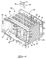
- FIGS 12-15 illustrate another alternative receptacle embodiment 412 wherein the housing means is comprised of first and second housing members 414a and 414b, which together define elongate cavities 436 extending between corresponding sides 424 and 434 of first and second housing members 414a,414b respectively, as best seen in Figure 15.
- Housing members 414a and 414b are securable together along their respective longitudinal sides by respective interlocking "teeth" 426,435 and at the ends by interlocking teeth and groves, 431a,431b.
- First housing member 414a corresponds to the inner housing portion of the previously described embodiments and includes mating face 416, mounting face 418, side walls 424 and end walls 428.
- a plurality of spaced outwardly projecting teeth 426 extend along the outer surface of wall 424 proximate mounting face 418.
- a plurality of first terminal members 440 having first and second connecting portions 442,444, respectively are disposed in respective terminal-receiving passageways 432.
- Second housing member 414b is essentially a shell member having longitudinally extending side walls 434, end walls 433, and a plurality of terminal-receiving passageways 438 for receiving second terminal members 446 therein.
- Second terminal members 446 include first contact section 448 having an arcuate portion 449 adjacent free end 447 and second contact section 452 extending through lower second housing wall 421.
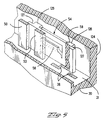
- FIG. 15 The assembled receptacle 412 having a shunt terminal member 454 is shown in Figure 15.
- Figures 13 and 14 show enlarged views of the respective interlocked walls 424,434 at a shunt location.
- Selected teeth 426 along wall 424 are provided with slots 427 for receiving ends of shunt terminal members 454 in a manner similar to that previously described.
- Housing wall 424 as shown in Figure 14, includes two such teeth 426 having a shunt terminal 454 disposed therebetween. Tooth 426a intermediate the modified teeth 426 has been shortened to accommodate the outwardly projecting contact surface 456 of shunt terminal 454.
- the inner surfaces of wall 434 includes teeth 435 that are adapted to interlock with first housing member teeth 426 to secure the first and second housings together.
- This figure also shows the shortening of two of the teeth 435a at a shunt terminal location to accommodate the shape of the shunt terminal.
- the housing members of the present invention are molded from a suitable dielectric material such as a glass-filled polyester or the like.
- the first and second terminal members are from a material having high spring characteristics such as stamped and formed phosphor bronze or the like. Since the third terminal members are not spring members they may be formed of brass or other suitable materials.
- Ground shields or plate members 84,90 are preferably made from a high conductivity brass.
- the shunt terminal members are made from beryllium copper.
- Second terminal members are inserted into terminal-receiving passageways from the mating face and are secured therein as known in the art. If desired, shunt contact are inserted at the appropriate locations along the housing sidewalls.
- the receptacle of Figures 12-15 is assembled by loading the first and second terminals into their respective terminal-receiving passageways and any shunt contacts into their respective locations.
- the two housing members are assembled by engaging the teeth along the sidewalls and sliding the members together.
- the assembled receptacle member can then be mounted to a board 102 by inserting respective second contact sections of the first and second terminal members into corresponding board apertures and are held thereon by appropriate means.
- Pin header 60 is assembled by inserting third terminal members 78 into slots 77 along wall 70 of housing 62.
- the first and second ground plates 84,90 are assembled to housing 62 by inserting respective 85,91 into associated slots 75 to flanges 74.
- the plate members 84,90 it is preferable to include a plurality of second contact sections 84,90 respectively thereby providing multiple parallel paths to ground, thus lowering the inductance and resistance to ground.
- the number of outwardly extending second ground contact sections 88,94 of the plates 84,90 correspond to the number of columns of third terminal members 68 in the pin header 60 and the corresponding second terminal members 46 of the receptacle member 12 correspond to the columns of first terminal members 40 within the receptacle housing 14.
- the present invention provides a number of advantages for board to board connector systems. As is shown in the drawings a connector system is compatible with existing ungrounded/shielded connectors thereby permitting the user to gradually upgrade the system. Since the configuration of the basic pin header and basic receptacle member remains the same, both the enhanced and the standard pin header and receptacle member can be used interchangeably.
Description
- This invention relates to an electrical connector assembly for electrically interconnecting corresponding circuits between two circuit boards.
- Board to board connectors are used to interconnect circuitry on a plurality of daughter boards to a mother board or backplane. These boards may be mounted in a vertical or horizontal relationship depending upon the configuration of the mating connector members.
- The demand for connectors that solve problems such as common mode noise and crosstalk has increased with the density and speed of electronic circuitry. It is desirable, therefore, to provide high density electrical connectors with means to provide a low inductance and low resistance ground connection from the connector to the circuit board to which it is attached.
- U.S. Patent 4,867,690 discloses an electrical connector system comprising a pin header having a plurality of rows of terminal members extending parallel to the sidewalls. The outermost rows of terminals adjacent the sidewalls are adapted to provide ground reference paths while the remaining rows of terminals are adapted to be mated to a receptacle member.
- U.S. Patent 4,655,518 discloses an electrical connector and a two-piece connector assembly providing grounding contacts along the dielectric sidewalls of the respective connectors. The terminal members of the pin header are positioned in recesses along the inside surfaces of the sidewall with the contact portion being a convex shape single resilient beam facing inwardly toward the pin terminals positioned between the sidewalls. In the receptacle member, ground contacts are placed along the outside surfaces of the sidewall so that they will slidably engage resilient beams in the pin header when the connectors are mated.
- It is also desirable in certain applications to provide means for shorting together any two adjacent electrical contacts when a mating connector and board is removed from a system thereby providing a switching effect to maintain electrical continuity of the system. The "built in" switches eliminate the need for additional parts to provide the same capability.
- For high density, high speed electronic systems it is generally desirable to provide means for shielding modules within the system for protection from EMI/RFI. It is desirable, therefore, that connector assemblies used within the system include means for facilitating interconnection of module shields to ground planes within the mother board or backplane. For purposes of this application, the terms "shielded pin header", "shielded receptacle" or "shielded connector assembly" are to be understood to mean members having a ground plate or other structure that provides the above described capability.
- Furthermore, it is desirable that the mating members of grounded or shielded connector assembly also be matable with respective existing complementary non-grounded or shielded members to provide a cost effective manner of upgrading existing electronic systems such as computers and instrumentation.
- The present invention is directed to an electrical connector system that eliminates the problems and disadvantages of the prior art and consists in an electrical connector according to
claim 1 and in an electrical connector assembly according to claim 3. - FR 2590415 discloses an electrical connector and an electrical connector assembly according to the preambles of
claims 1 and 3. - The invention enables an improvement in the electrical performance of the connector by providing additional low inductance and low resistance paths for ground current to flow through the electrical connector assembly to a circuit board. Moreover, it can provide a shielded connector system that is also compatible with existing unshielded connectors.
- According to a feature of the invention, means may be provided for shunting or switching adjacent contact terminals to provide electrical continuity upon removal of a board from a system, thereby eliminating the need to use additional components to provide the same function.
- Embodiments of the invention will now be described by way of example with reference to the accompanying drawings in which:
- FIGURE 1 is an enlarged fragmentary perspective view of the electrical connector assembly of the present invention with the receptacle and pin header members exploded from one another.
- FIGURE 2 is a cross sectional view of the connector assembly of the invention with the members exploded from each other.
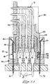
- FIGURE 3 is a cross sectional view of the mated connector assembly with the members mated.
- FIGURE 4 is an enlarged fragmentary portion of an alternative embodiment of the receptacle member with a shunt terminal exploded therefrom.
- FIGURE 5 is enlarged portion of the receptacle member of Figure 4 illustrating the means for securing a shunt terminal to the housing sidewall.
- FIGURE 6 is a fragmentary portion of the pin header member of the present invention with one of the ground plate shields exploded therefrom.
- FIGURE 7 is an enlarged fragmentary portion of Figure 6 illustrating the means for securing the ground plate to the pin header.
- FIGURE 8 is fragmentary perspective view of an alternative embodiment of the pin header for use with the receptacle member of Figure 4.
- FIGURE 9 is a cross sectional view of the receptacle member of Figure 4 mated with the pin header of Figure 8.
- FIGURE 10 is fragmentary perspective view of a pin header illustrating an alternative embodiment of the invention.
- FIGURE 11 is a cross sectional view of the receptacle of the present invention mated to an unshielded pin header member.
- FIGURE 12 is an exploded perspective view of a further alternative embodiment of the receptacle member.
- FIGURES 13 and 14 are enlarged views of portions of the receptacle member of Figure 12.
- FIGURE 15 is a cross sectional view of the assembled receptacle member of Figure 12.
-
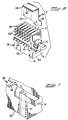
- Referring now to Figures 1, 2 and 3, the
connector assembly 10 of the present invention comprises areceptacle member 12 and apin header 60. For purposes of illustrating the invention, the board toboard connector assembly 10 is shown in a configuration suitable for mounting daughter cards perpendicular to the mother board or backplane. It is to be understood that the pin header member can be modified for positioning the daughter cards in parallel with the mother board.Receptacle member 12 includes ahousing member 14 having amating face 16 and amounting face 18.Housing 14 has atransverse body section 20 extending along themounting face 18 as best seen in Figure 4, aninner body portion 22 and opposedouter side walls 34 extending from mountingface 18 to matingface 16 and definingelongate cavities 36 between theinner body portion 22 and respectiveouter side walls 34.Inner body portion 22 includesopposed side walls 24,end walls 28 having mountingflanges 30 extending outwardly therefrom, and a plurality of terminal-receivingpassageways 32 extending from themounting face 18 to themating face 16. A plurality of firstcontact terminal members 40 are disposed inrespective passageways 32, as shown in Figures 2 and 3. For purposes of illustration,first terminal members 40 have been eliminated in Figures 1 and 4.First terminal members 40 include afirst contact section 42 for mating withcomplementary terminal members 78 ofpin header 60 and asecond contact section 44 extending below themounting face 18 for engagement withcorresponding apertures 104 of thecircuit board 102. - As seen in Figures 1-3
elongate cavities 36 are defined along thin sides by the inner surface ofouter side walls 34 and the corresponding outer surfaces ofbody side walls 24 and the respective portions oftransverse wall 20 extending therebetweenforms cavity base 21.Cavity base 21 includes a plurality ofapertures 38 extending therethrough.Receptacle 12 further includes a plurality of secondcontact terminal members 46 disposed in terminal-receivingapertures 38 oftransverse wall 20 and havingfirst contact sections 48 extending intoelongate cavities 36 and asecond contact section 52 extending outwardly from mountingface 18 for engagement withapertures 106 of mother board orbackplane 102. As best seen in Figures 2 and 3,first terminal section 48 of respectivesecond contact terminals 46 include cantilevered beam portions having an inwardly directedarcuate section 49 and acontact surface 50 intermediatearcuate section 49 andsecond contact section 52. Correspondingcontact surfaces 50 ofsecond terminal members 46 are adapted to mate with corresponding ground bus means 84,90 of thecomplementary mating connector 60 as shown in Figure 3. - Figures 4 and 5 illustrate an alternative
receptacle member embodiment 120, which includes at least oneshunt terminal member 54 to provide an internal "switching effect." Since the basic structure ofreceptacle member 120 is essentially the same as that ofreceptacle member 12, the same reference numerals have been used for the identical parts.Receptacle member 120 includes ahousing member 140 having atransverse body section 20 extending along themounting face 18 as best seen in Figure 4, aninner body portion 122 and opposedouter side walls 34 extending upward from themounting face 18 and definingelongate cavities 36 between theinner body portion 122 and respectiveouter side walls 34.Inner body portion 122 includesopposed side walls 124,end walls 28 having mountingflanges 30 extending outwardly therefrom. In this embodiment, the outside surfaces ofside walls 124 ofinner body portion 122 further includeprojections 126 extending intorespective cavities 36 at selected locations therealong.Projections 126 includeslots 127 for receiving ashunt terminal member 54 therebetween. Shuntterminal member 54 includes an outwardly extendingportion 56 andends 58, theends 58 being received inprojection slots 127 and extending between two adjacentsecond terminal members 46. As shown in Figure 5,shunt terminal member 54 electrically interconnects two adjacentsecond terminal members 46 within arespective cavity 36, when thereceptacle member 120 is not mated to a complementary connector. - Referring again to Figures 1-3, the
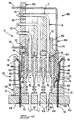
pin header 60 of the present invention includes ahousing 62 having amating face 64 and mountingface 68.Cavity 66, configured to receiveinner housing 22 ofmating receptacle 12 therein, extends inwardly frommating face 64. For purposes of illustration,pin header 60 is shown in a right angle configuration for mounting to adaughter card 108.Pin header 60 includesside wall 70 opposed to mountingface 68,back wall 71 opposed tomating face 64, and opposedend walls 72 having outwardly extendingflanges 74 thereon.Housing 62 further includes a plurality of terminal-receivingpassageways 76 extending through thehousing 62 and between the mating andmounting faces third terminal members 78 having first andsecond contact sections passageways 76. As shown more clearly in Figure 6, the terminal-receivingpassageways 76 includeslots 77 along theback wall 71 for assembling respectivethird terminal members 78 into thehousing 62.First contact section 80 of eachthird terminal member 78 is shown as a pin member adapted for mating with a complementaryfirst terminal member 40 and second contact section is adapted for mounting to correspondingapertures 110 ofdaughter card 108.Pin header 60 further includes first and second ground or shield plate means 84,90 disposed on outer surfaces of the connector with first ground plate means 84 extending alongback wall 71 andside wall 70. Thefirst ground plate 84 includes first and second connectingportions ground connecting portion 86 being adapted for electrical connection with the secondterminal members 46 in one of thecavities 36 ofreceptacle 12, as best seen in Figure 3. Thesecond ground plate 90 extends along the forwardly projecting portion of mountingface 68 ofpin header 60 and is adapted to be received within the other of theelongate cavities 36 of thecorresponding receptacle member 12 and to be electrically engaged to the plurality ofsecond contact members 46 therein. As best seen in Figures 6 and 7 theground plate members tabs slots 75 in the outwardly extendingflanges 74 to secure theground plates housing member 62. - As shown in Figures 2 and 3 when
pin header 60 is mated to thereceptacle member 12 the outwardly extendingcontacts ground plates pin header 60 will engage the correspondingground contact terminals 46 of thereceptacle member 12 prior to engagement of the respectivefirst contact sections terminal members first contact sections ground plates respective cavities 36, outwardly deflect the cantilevered arms of secondterminal members 46 and electrically engage the corresponding contact surfaces 50 of the secondterminal members 46 within therespective cavities 36. Concomitantly herewith, the thirdterminal members 78 become fully mated with the corresponding firstterminal members 40. The continuous shield on the outer surfaces of thepin header 60 facilitates interconnection to ground planes in the mother board or backplane and to shielding means in those applications where EMI/RFI protection is desired. - Figures 8 and 9 illustrate alternative
pin header embodiment 160 for mating withreceptacle member 120 of Figure 4 having at least oneshunt terminal member 54 disposed along aside wall 124. In thisembodiment wall 170 of pinheader housing member 162 includes at least oneprojection 171 extending outwardly therefrom at a location selected to correspond to the location of theshunt terminal member 54 ofreceptacle member 120 of Figure 4.First plate member 184 includes at least oneslot 187 extending thereinto from the edge of thefirst contact portion 186 at a location selected to correspond to the location ofshunt terminal member 54 ofreceptacle member 120. - As shown in Figure 9 when
pin header 160 is mated to thereceptacle member 120, the outwardly extendingcontacts ground plates pin header 60 will engage the correspondingground contact terminals 46 of thereceptacle member 120 prior to engagement of the respectivefirst contact sections terminal members projection 171 ofhousing member 162 disengages shuntterminal member 54 from engagement with the associated secondterminal members 46 by deflecting the corresponding cantilevered arms outwardly and into the correspondingcavities 36. Slot 187 ofplate 186 is of sufficient size to prevent engagement ofplate member 186 with the formerly shunted second terminal members, thereby establishing switching capability for the connector assembly. The remaining terminal members electrically engaged their respective counterparts as previously described. - Figure 10 shows a further alternative
pin header embodiment 260 whereinfirst plate member 284 includes a plurality ofsegments 285, each including at least oneaperture 287 therein for cooperating with projection means 271 on awall 270 of pin header housing member 262.Wall 270 further includes a plurality ofspacer members 273, which aid in keepingshield segments 285 from rotating. In the preferredembodiment plate segments 285 are heat staked to the housing wall. Only the second corresponding receptacle terminal members 46 (as shown in Figure 1) associated with eachindividual segment 285 are commoned. By using a plurality of plate segments the individual segments can be used for interconnection of either signal, ground or power circuits, thereby increasing the capability of the connector assembly. - As is shown in Figure 11, the
receptacle 12 of the present invention is intermatable with anunshielded pin header 360 as well as the grounded or shieldedpin header 60 of the present invention. When receptaclemember 12 is mated with theunshielded pin header 160 presently available, thearcuate portion 49 of each of the secondterminal members 46 engage the outer surface ofdielectric housing 162. Theelectrical contact region 50 ofreceptacle member 12 is, therefore, protected from accumulating films or debris from the dielectric housing walls of theunshielded pin header 160. Thus, thesame receptacle member 12 can be mated interchangeably with a shielded or grounded pin header or unshielded pin header 60,160. Any buildup of dielectric material on thesecond contact terminal 46 occurs at thearcuate portion 49 rather than thecontact section 50. - Figures 12-15 illustrate another
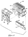
alternative receptacle embodiment 412 wherein the housing means is comprised of first andsecond housing members elongate cavities 436 extending between correspondingsides second housing members Housing members First housing member 414a corresponds to the inner housing portion of the previously described embodiments and includesmating face 416, mountingface 418,side walls 424 and endwalls 428. A plurality of spaced outwardly projectingteeth 426 extend along the outer surface ofwall 424 proximate mountingface 418. A plurality of firstterminal members 440 having first and second connecting portions 442,444, respectively are disposed in respective terminal-receivingpassageways 432.Second housing member 414b is essentially a shell member having longitudinally extendingside walls 434, endwalls 433, and a plurality of terminal-receivingpassageways 438 for receiving secondterminal members 446 therein. Secondterminal members 446 includefirst contact section 448 having anarcuate portion 449 adjacentfree end 447 andsecond contact section 452 extending through lowersecond housing wall 421. - The assembled
receptacle 412 having ashunt terminal member 454 is shown in Figure 15. Figures 13 and 14 show enlarged views of the respective interlocked walls 424,434 at a shunt location. Selectedteeth 426 alongwall 424 are provided withslots 427 for receiving ends ofshunt terminal members 454 in a manner similar to that previously described.Housing wall 424 as shown in Figure 14, includes twosuch teeth 426 having ashunt terminal 454 disposed therebetween.Tooth 426a intermediate the modifiedteeth 426 has been shortened to accommodate the outwardly projecting contact surface 456 ofshunt terminal 454. As seen more clearly in Figure 13, the inner surfaces ofwall 434 includesteeth 435 that are adapted to interlock with firsthousing member teeth 426 to secure the first and second housings together. This figure also shows the shortening of two of theteeth 435a at a shunt terminal location to accommodate the shape of the shunt terminal. - The housing members of the present invention are molded from a suitable dielectric material such as a glass-filled polyester or the like. The first and second terminal members are from a material having high spring characteristics such as stamped and formed phosphor bronze or the like. Since the third terminal members are not spring members they may be formed of brass or other suitable materials. Ground shields or
plate members board 102 by inserting respective second contact sections of the first and second terminal members into corresponding board apertures and are held thereon by appropriate means. -
Pin header 60 is assembled by inserting thirdterminal members 78 intoslots 77 alongwall 70 ofhousing 62. The first andsecond ground plates housing 62 by inserting respective 85,91 into associatedslots 75 to flanges 74. - In forming the
plate members second contact sections - In the preferred embodiment the number of outwardly extending second
ground contact sections plates terminal members 68 in thepin header 60 and the corresponding secondterminal members 46 of thereceptacle member 12 correspond to the columns of firstterminal members 40 within thereceptacle housing 14. The present invention provides a number of advantages for board to board connector systems. As is shown in the drawings a connector system is compatible with existing ungrounded/shielded connectors thereby permitting the user to gradually upgrade the system. Since the configuration of the basic pin header and basic receptacle member remains the same, both the enhanced and the standard pin header and receptacle member can be used interchangeably.
Claims (7)
- An electrical connector comprising an elongate housing means (14) having a mating face (16) and a mounting face (18), and a transverse body section (20) extending along the mounting face (18), said transverse body section including an inner body portion (22) and outer side walls (34) extending from the mounting face (18) to the mating face (16) and defining cavity means (36) between the inner body portion (22) and the outer side walls (34), said inner body portion (22) having a plurality of terminal receiving passageways (32) extending therethrough and arranged in rows longitudinally of the housing means, a plurality of first terminal members (40) disposed in respective passageways (32) for mating with complementary terminal members of a complementary mating connector, and second discrete terminal members (46) disposed in the transverse body section (20) and having terminal sections extending into the cavity means for mating with ground bus means of the complementary mating connector, characterised in thatthe cavity means consists of only two elongate cavities (36) extending longitudinally of the housing means between the inner body portion (22) and two opposed outer side walls (34) spaced from the inner body portion and extending longitudinally of the housing,and in that a plurality of the second contact terminal members (46) is disposed in each of the cavities (36), said second contact terminal members having first contact sections (48) extending into the cavities which are cantilevered beam portions having inwardly directed arcuate sections (49).
- The connector of claim 1, including at least one shunt terminal member (54) arranged to common at least two of the second contact terminal members (46).
- An electrical connector assembly (10) comprising a receptacle member (12) and a complementary mating pin header (60), the receptacle member including an elongate housing means (14) having a mating face (16) and a mounting face (18) and a transverse body section (20) extending along the mounting face, said transverse body section including an inner body portion (22) and outer side walls (34) extending from the mounting face (18) to the mating face (16) and defining cavity means (36) between the inner body portion (22) and the outer side walls (34), said inner body portion having a plurality of terminal receiving passageways (32) extending therethrough and arranged in rows longitudinally of the housing means, a plurality of first terminal members (40) disposed in the respective passageways (32) for mating with complementary terminal members of the mating pin header (60), and second discrete contact terminal members (46) disposed in the transverse body section (20) and having terminal sections extending into the cavity means for mating with ground bus means of the mating pin header; and the pin header (60) including a housing member (62) having a mating face (64), a mounting face (68), opposed sides, a plurality of terminal receiving passageways (76) extending through the housing member, and a plurality of other electrical contact terminal members (78) disposed in respective terminal receiving passageways (76) for mating with the first terminal members (40);the connector assembly (10) being characterised in thatthe cavity means of the receptacle housing means (14) consists of only two elongate cavities (36) extending longitudinally of the housing means between the inner body portion (22) and two opposed outer side walls (34) spaced from the inner body portion and extending longitudinally of the housing,a plurality of the second contact terminal members (46) is disposed in each of the cavities (36), said second contact terminal members having first contact sections (48) extending into the cavities which are cantilevered beam portions having inwardly directed arcuate sections (49); andground members (84,90) disposed along opposite sides of the pin header housing member (60), said ground members (84,90) being receivable in the elongate cavities (36) of the receptacle member (12) when the receptacle member (12) and the pin header (60) are mated, and the ground members being disposed at selected locations opposing the second contact terminal members (46) of the receptacle member (12) to electrically engage therewith upon mating.
- The connector assembly (10) of claim 3, wherein at least one ground member (84) defines a bus means and extends continuously along at least one side of said pin header.
- The connector assembly of claim 3 or 4, wherein at least one ground member comprises a plurality of segments (284), whereby selected groups of associated second terminal members (46) of the receptacle (12) are commoned.
- The connector assembly of claim 3, 4 or 5, including at least one shunt terminal member (54) arranged to electrically common at least two of the second terminal members (46) of said receptacle member (12).
- The connector assembly of claim 3, wherein the body portion (22) of the receptacle member (12) includes means for securing a shunt terminal member (54) thereto, the shunt terminal member (54) being arranged to electrically common at least two adjacent second terminal members (46) when the receptacle member (12) is not mated to the pin header (60).
Applications Claiming Priority (2)
| Application Number | Priority Date | Filing Date | Title |
|---|---|---|---|
| US58636090A | 1990-09-21 | 1990-09-21 | |
| US586360 | 1990-09-21 |
Publications (4)
| Publication Number | Publication Date |
|---|---|
| EP0476883A2 EP0476883A2 (en) | 1992-03-25 |
| EP0476883A3 EP0476883A3 (en) | 1992-10-14 |
| EP0476883B1 EP0476883B1 (en) | 1995-10-25 |
| EP0476883B2 true EP0476883B2 (en) | 2000-12-20 |
Family
ID=24345430
Family Applications (1)
| Application Number | Title | Priority Date | Filing Date |
|---|---|---|---|
| EP91308042A Expired - Lifetime EP0476883B2 (en) | 1990-09-21 | 1991-08-30 | Electrical connector assembly |
Country Status (4)
| Country | Link |
|---|---|
| EP (1) | EP0476883B2 (en) |
| JP (1) | JP3194603B2 (en) |
| KR (1) | KR970004153B1 (en) |
| DE (1) | DE69114094T2 (en) |
Families Citing this family (10)
| Publication number | Priority date | Publication date | Assignee | Title |
|---|---|---|---|---|
| EP0540310B1 (en) * | 1991-11-01 | 1996-07-03 | The Whitaker Corporation | Electrical connector having externally mounted ground plates |
| US5403206A (en) * | 1993-04-05 | 1995-04-04 | Teradyne, Inc. | Shielded electrical connector |
| FR2707046A1 (en) * | 1993-04-05 | 1994-12-30 | Teradyne Inc | |
| DE19640847B4 (en) * | 1996-10-03 | 2007-03-08 | Amp-Holland B.V. | Right Angle Shielded Electrical Connector |
| JPH118027A (en) * | 1997-06-13 | 1999-01-12 | Sumitomo Wiring Syst Ltd | Connector for substrate |
| AU8030998A (en) * | 1997-07-10 | 1999-02-08 | Whitaker Corporation, The | Apparatus for forming a connection through a board |
| DK174367B1 (en) * | 1999-12-30 | 2003-01-13 | Lk As | Electric circuit board as well as multi connectors |
| JP4669824B2 (en) * | 2006-08-07 | 2011-04-13 | 任天堂株式会社 | connector |
| DE102011006934A1 (en) * | 2011-04-07 | 2012-10-11 | Robert Bosch Gmbh | Electrical plug-in device with leading contact |
| JP6140473B2 (en) * | 2013-02-27 | 2017-05-31 | 矢崎総業株式会社 | Shield connector and shield connector connection structure |
Family Cites Families (4)
| Publication number | Priority date | Publication date | Assignee | Title |
|---|---|---|---|---|
| US4869677A (en) * | 1984-08-17 | 1989-09-26 | Teradyne, Inc. | Backplane connector |
| US4601527A (en) * | 1985-01-18 | 1986-07-22 | E. I. Du Pont De Nemours And Company | Shielded header and cable assembly |
| DE3787270T2 (en) * | 1986-12-22 | 1994-03-31 | Whitaker Corp | High density coaxial connector. |
| US4867690A (en) * | 1988-06-17 | 1989-09-19 | Amp Incorporated | Electrical connector system |
-
1991
- 1991-08-30 EP EP91308042A patent/EP0476883B2/en not_active Expired - Lifetime
- 1991-08-30 DE DE69114094T patent/DE69114094T2/en not_active Expired - Lifetime
- 1991-09-16 KR KR1019910016084A patent/KR970004153B1/en not_active IP Right Cessation
- 1991-09-20 JP JP26863891A patent/JP3194603B2/en not_active Expired - Lifetime
Also Published As
| Publication number | Publication date |
|---|---|
| KR970004153B1 (en) | 1997-03-25 |
| DE69114094D1 (en) | 1995-11-30 |
| DE69114094T2 (en) | 1996-05-30 |
| EP0476883B1 (en) | 1995-10-25 |
| KR920007264A (en) | 1992-04-28 |
| EP0476883A2 (en) | 1992-03-25 |
| JPH04255678A (en) | 1992-09-10 |
| EP0476883A3 (en) | 1992-10-14 |
| JP3194603B2 (en) | 2001-07-30 |
Similar Documents
| Publication | Publication Date | Title |
|---|---|---|
| US5104329A (en) | Electrical connector assembly | |
| US6435914B1 (en) | Electrical connector having improved shielding means | |
| EP0829930B1 (en) | Connector with integrated power leads | |
| EP0460976B1 (en) | Connectors with ground structure | |
| CA2166670C (en) | Shielded compact data connector | |
| US4975084A (en) | Electrical connector system | |
| US5586893A (en) | IC card connector shield grounding | |
| EP0405454B1 (en) | Coaxial contact element | |
| EP0658953B1 (en) | Multi-port modular jack assembly | |
| EP0560550B1 (en) | Shielded back plane connector | |
| US6705902B1 (en) | Connector assembly having contacts with uniform electrical property of resistance | |
| EP0520283B1 (en) | Connectors with ground structure | |
| EP1356551B1 (en) | High-density receptacle connector | |
| US5135405A (en) | Connectors with ground structure | |
| EP0337634A1 (en) | A reference conductor for improving signal integrity in electrical connectors | |
| US20050227514A1 (en) | Power connector with safety feature | |
| EP1356549A1 (en) | Connector interface and retention system for high-density connector | |
| US7976321B2 (en) | Electrical connector with a ground terminal | |
| EP0365179B1 (en) | Electrical connector system | |
| US6296518B1 (en) | Stacked electrical connector assembly | |
| EP0476883B2 (en) | Electrical connector assembly | |
| EP0850499B1 (en) | Shielded electrical connector | |
| US5174771A (en) | Electrical connector having externally mounted ground plates | |
| EP0540310B1 (en) | Electrical connector having externally mounted ground plates |
Legal Events
| Date | Code | Title | Description |
|---|---|---|---|
| PUAI | Public reference made under article 153(3) epc to a published international application that has entered the european phase |
Free format text: ORIGINAL CODE: 0009012 |
|
| AK | Designated contracting states |
Kind code of ref document: A2 Designated state(s): DE FR GB IT NL |
|
| PUAL | Search report despatched |
Free format text: ORIGINAL CODE: 0009013 |
|
| AK | Designated contracting states |
Kind code of ref document: A3 Designated state(s): DE FR GB IT NL |
|
| RAP1 | Party data changed (applicant data changed or rights of an application transferred) |
Owner name: THE WHITAKER CORPORATION |
|
| 17P | Request for examination filed |
Effective date: 19930402 |
|
| 17Q | First examination report despatched |
Effective date: 19941012 |
|
| GRAA | (expected) grant |
Free format text: ORIGINAL CODE: 0009210 |
|
| AK | Designated contracting states |
Kind code of ref document: B1 Designated state(s): DE FR GB IT NL |
|
| ITF | It: translation for a ep patent filed |
Owner name: BUZZI, NOTARO&ANTONIELLI D'OULX |
|
| REF | Corresponds to: |
Ref document number: 69114094 Country of ref document: DE Date of ref document: 19951130 |
|
| ET | Fr: translation filed | ||
| PLBI | Opposition filed |
Free format text: ORIGINAL CODE: 0009260 |
|
| PLBF | Reply of patent proprietor to notice(s) of opposition |
Free format text: ORIGINAL CODE: EPIDOS OBSO |
|
| 26 | Opposition filed |
Opponent name: SIEMENS AG GR PA 6 Effective date: 19960725 |
|
| NLR1 | Nl: opposition has been filed with the epo |
Opponent name: SIEMENS AG GR PA 6 |
|
| PLBF | Reply of patent proprietor to notice(s) of opposition |
Free format text: ORIGINAL CODE: EPIDOS OBSO |
|
| PLBF | Reply of patent proprietor to notice(s) of opposition |
Free format text: ORIGINAL CODE: EPIDOS OBSO |
|
| PLBF | Reply of patent proprietor to notice(s) of opposition |
Free format text: ORIGINAL CODE: EPIDOS OBSO |
|
| PLAW | Interlocutory decision in opposition |
Free format text: ORIGINAL CODE: EPIDOS IDOP |
|
| APAC | Appeal dossier modified |
Free format text: ORIGINAL CODE: EPIDOS NOAPO |
|
| APAE | Appeal reference modified |
Free format text: ORIGINAL CODE: EPIDOS REFNO |
|
| APAC | Appeal dossier modified |
Free format text: ORIGINAL CODE: EPIDOS NOAPO |
|
| PLBQ | Unpublished change to opponent data |
Free format text: ORIGINAL CODE: EPIDOS OPPO |
|
| PLAB | Opposition data, opponent's data or that of the opponent's representative modified |
Free format text: ORIGINAL CODE: 0009299OPPO |
|
| R26 | Opposition filed (corrected) |
Opponent name: SIEMENS AG GR PA 6 Effective date: 19960725 |
|
| APAC | Appeal dossier modified |
Free format text: ORIGINAL CODE: EPIDOS NOAPO |
|
| NLR1 | Nl: opposition has been filed with the epo |
Opponent name: SIEMENS AG GR PA 6 |
|
| PLAW | Interlocutory decision in opposition |
Free format text: ORIGINAL CODE: EPIDOS IDOP |
|
| PUAH | Patent maintained in amended form |
Free format text: ORIGINAL CODE: 0009272 |
|
| STAA | Information on the status of an ep patent application or granted ep patent |
Free format text: STATUS: PATENT MAINTAINED AS AMENDED |
|
| 27A | Patent maintained in amended form |
Effective date: 20001220 |
|
| AK | Designated contracting states |
Kind code of ref document: B2 Designated state(s): DE FR GB IT NL |
|
| RIC2 | Information provided on ipc code assigned after grant |
Free format text: 7H 01R 13/658 A, 7H 01R 12/18 B, 7H 01R 12/20 B |
|
| ITF | It: translation for a ep patent filed |
Owner name: BUZZI, NOTARO&ANTONIELLI D'OULX |
|
| NLR2 | Nl: decision of opposition | ||
| NLR3 | Nl: receipt of modified translations in the netherlands language after an opposition procedure | ||
| ET3 | Fr: translation filed ** decision concerning opposition | ||
| REG | Reference to a national code |
Ref country code: GB Ref legal event code: IF02 |
|
| APAH | Appeal reference modified |
Free format text: ORIGINAL CODE: EPIDOSCREFNO |
|
| PGFP | Annual fee paid to national office [announced via postgrant information from national office to epo] |
Ref country code: NL Payment date: 20100824 Year of fee payment: 20 |
|
| PGFP | Annual fee paid to national office [announced via postgrant information from national office to epo] |
Ref country code: FR Payment date: 20100831 Year of fee payment: 20 Ref country code: DE Payment date: 20100827 Year of fee payment: 20 Ref country code: IT Payment date: 20100826 Year of fee payment: 20 |
|
| PGFP | Annual fee paid to national office [announced via postgrant information from national office to epo] |
Ref country code: GB Payment date: 20100825 Year of fee payment: 20 |
|
| REG | Reference to a national code |
Ref country code: DE Ref legal event code: R071 Ref document number: 69114094 Country of ref document: DE |
|
| REG | Reference to a national code |
Ref country code: DE Ref legal event code: R071 Ref document number: 69114094 Country of ref document: DE |
|
| REG | Reference to a national code |
Ref country code: NL Ref legal event code: V4 Effective date: 20110830 |
|
| REG | Reference to a national code |
Ref country code: GB Ref legal event code: PE20 Expiry date: 20110829 |
|
| PG25 | Lapsed in a contracting state [announced via postgrant information from national office to epo] |
Ref country code: GB Free format text: LAPSE BECAUSE OF EXPIRATION OF PROTECTION Effective date: 20110829 |
|
| PG25 | Lapsed in a contracting state [announced via postgrant information from national office to epo] |
Ref country code: NL Free format text: LAPSE BECAUSE OF EXPIRATION OF PROTECTION Effective date: 20110830 |
|
| PG25 | Lapsed in a contracting state [announced via postgrant information from national office to epo] |
Ref country code: DE Free format text: LAPSE BECAUSE OF EXPIRATION OF PROTECTION Effective date: 20110831 |