EP0476817B1 - Verfahren und Vorrichtung zur digitalen Verarbeitung des Gammas, des Schwarzwertes und des Verstärkungsfaktors - Google Patents
Verfahren und Vorrichtung zur digitalen Verarbeitung des Gammas, des Schwarzwertes und des Verstärkungsfaktors Download PDFInfo
- Publication number
- EP0476817B1 EP0476817B1 EP91307122A EP91307122A EP0476817B1 EP 0476817 B1 EP0476817 B1 EP 0476817B1 EP 91307122 A EP91307122 A EP 91307122A EP 91307122 A EP91307122 A EP 91307122A EP 0476817 B1 EP0476817 B1 EP 0476817B1
- Authority
- EP
- European Patent Office
- Prior art keywords
- value
- values
- gamma
- black level
- level
- Prior art date
- Legal status (The legal status is an assumption and is not a legal conclusion. Google has not performed a legal analysis and makes no representation as to the accuracy of the status listed.)
- Expired - Lifetime
Links
Images


Classifications
-
- H—ELECTRICITY
- H04—ELECTRIC COMMUNICATION TECHNIQUE
- H04N—PICTORIAL COMMUNICATION, e.g. TELEVISION
- H04N5/00—Details of television systems
- H04N5/14—Picture signal circuitry for video frequency region
- H04N5/20—Circuitry for controlling amplitude response
- H04N5/202—Gamma control
-
- H—ELECTRICITY
- H04—ELECTRIC COMMUNICATION TECHNIQUE
- H04N—PICTORIAL COMMUNICATION, e.g. TELEVISION
- H04N5/00—Details of television systems
- H04N5/14—Picture signal circuitry for video frequency region
- H04N5/20—Circuitry for controlling amplitude response
Definitions
- This invention relates to a method and apparatus for gamma correction and independent modification of black and white (pedestal and gain, respectively) levels.
- gamma correction is accomplished by implementing a piecewise (step-by-step) linear transfer function utilizing a load resistor network for a transistor.
- the network is interconnected with diodes to provide a plurality of gain break points at particular pre-determined voltage values.
- a gain/voltage characteristic is generated by the gamma corrector and is selected to compensate for the non-linearities of the transducer (e.g. camera or monitor). While this yields an acceptable gamma curve, it does not operate effectively when used in systems requiring the matching of several channels, for example, in a color television channel having red, green and blue channels.
- the result of gamma correction mismatch is a color shift for various signal amplitudes. This is most noticeable on monochrome signals which appear in color if the gain of all three channels is not the same.
- gamma values can be made variable using a plurality of resistors of different values, but the resolution of such systems is limited by the number of resistors available in the circuit.
- the gamma correction circuit is still an analog circuit and therefore includes the inherent stability problems of such analog circuits.
- Analog gamma correctors are made with transistor amplifiers and use resistor-diode combinations to set the various gain break points. Temperature and component age affect these components such that their characteristics do not remain constant.
- Digital gamma correctors are also known in the art. It is known, for example, to input data relating to a desired transfer characteristic into a random access memory (RAM) and then, using the data stored in the RAM, to make adjustments to the video signal. See, for example, US-A-4,394,688 to Iida et al. (hereinafter, "Iida”) and US-A-4,786,968 to Kutner (hereinafter, "Kutner”). US-A-4,568,978 to Cosh teaches “real time" gamma correction without the use of RAMs.
- EP-A-0 088 583 also discloses an apparatus and method according to the preamble of claims 1 and 5.
- the gamma value level is not the only value that is of concern to users of television systems.
- the black level, or pedestal, and the white level, or gain, are also signals that affect the sianal and which are routinely adjusted in the generation of a television signal.
- N 256 for an eight bit system
- BL is a value representing a desired black level
- WL is a value representing a desired white level
- F1 is the LOG of the result of the equation following in parentheses
- F2 is the ANTI-LOG of the result of the equation following in brackets
- gamma is the desired qamma value.
- a hardware embodiment of the present invention includes a digital aamma correction circuit which also allows independent modification of black and white levels (pedestal and gain).
- the value of gamma is continuously variable within the resolution of the number of bits used in the circuitry.
- a single RAM look-up table (LUT) is loaded with data representing the calculated values for desired qamma, black level and white level. If the black level of an incoming video signal is too high (high gain), it can be reduced along the curve of the gamma characteristic. Likewise, if the white level of the incoming video is too low (low gain), it may be increased along the curve of the gamma characteristic while leaving the black level fixed, thus raising the video gain.
- the transfer characteristic can be down-loaded from a controller, for example, a microprocessor or discrete control logic.
- the controller calculates the values to be loaded into the RAM using, for example, either equation (1) or (2), based upon desired values for black level, white level and gamma input by a system operator.
- the black level adjustment, white level adjustment and gamma correction are performed independently of each other, i.e., they do not interact with each other during camera set-up.
- the present invention takes advantage of the above-mentioned formulas to quickly compute the values for loading to the RAM with values at each address in the RAM corresponding to a particular desired gamma characteristic, black level and white level.
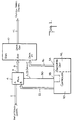
- FIG. 1 is a block diagram of an apparatus for gamma correction and black and white level modification according to the present invention.
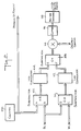
- FIG. 2 is a block diagram of an embodiment of the calculation unit of the controller of FIG. 1, which operates to compute values to be loaded into RAM in accordance with Equation (1).
- FIG. 3 is a block diagram of an embodiment of the calculation unit of the controller of FIG. 1, which operates to compute values to be loaded in RAM in accordance with Equation (2).
- FIG. 4 is a flow chart of a software implementation of the present invention using either Equation (1) or Equation (2).
- an incoming digital video signal is applied via input line 2 to input A of a multiplexer 4.
- Output 6 of multiplexer 4 is coupled via intermediate line 8 to ADD input of RAM 10.
- RAM 10 has a defined number of addresses, for example, 256 for an eight bit system.
- Data Out of RAM 10 is the output video signal which is gamma corrected and white and black level adjusted and is coupled to the output of the system for transmission to the television monitoring equipment via output video line 12.
- RAM 10 has been loaded with the desired parameters of gamma correction and white and black levels in accordance with either Equation (1) or Equation (2) at each of its addresses.
- the input video signal is applied to multiplexer 4 via input line 2, and is output directly to RAM 10 via intermediate line 8.
- the data therein acts upon the signal in a known manner to change the video signal and outputs the changed video signal to the output of the system via line 12. Since the present invention loads the addresses in RAM 10 with data relating to black level, white level and gamma, all three of those values of the input video signal are affected by the data in RAM 10. In other words, RAM 10 adjusts the values of black level, white level and gamma of the input video signals to the levels defined by the stored data.
- controller 20 is coupled to input B of multiplexer 4 via controller output line 22.
- Controller output 24 is coupled to the Data In terminal of RAM 10 via controller output line 26.
- Data select control 28 of controller 20 is manipulatable, either electronically or manually, by an operator of the system as desired to change the values of gamma, white level and/or black level for the system.
- Data select control 28 can comprise any selection means which allows a parameter to the adjusted and which actually adjust the parameter, for example, a selector switch in conjunction with a potentiometer, or an optical tach wheel which outputs pulses to increment or decrement a counter.
- multiplexer 4 is switched from input A to input B via A/B select line 30 upon receipt of a signal from the data select controller 28, which indicates that a parameter adjustment is to be made.
- Controller 20 senses the desired data change indicated by the degree of manipulation of data select control 28 and causes calculating unit 32 to calculate new values for the data to be changed for the addresses of RAM 10 in accordance with Equation 1, Equation 2, or other suitable equations. Controller 20 causes the new data to be loaded into RAM 10 via input B of multiplexer 4, reflecting the desired changes in the video input signal, as described more fully below.
- controller 20 switches multiplexer 4 from input B back to input A via a signal on A/B select line 30.
- RAM 10 then receives the input video signal and the new data in RAM 10 is used to process the incoming video signal so that the output video signal is corrected and adjusted for gamma, black and white levels, in accordance with the desires of the operator based on the new data in RAM 10.
- FIG. 2 is a block diagram of the preferred embodiment of a calculation unit 32 of controller 20 which performs the calculations set forth in Equation 1, above, Calculation unit 32 responds to manipulation by the operator data select control 28 and performs the actual calculation of the data to load into the RAM 10 to achieve the desired black level, white level, and gamma values.
- An address output from counter 100 is applied to RAM 10 via multiplexer 4 so that the inputs to the Data In terminal of RAM 10 are associated with the proper address.
- Counter 100 can comprise, for example, an eight bit address counter.
- a subtractor 102 also receives the output from counter 100, at input A.
- Input B of subtractor 102 receives a value BL indicative of the desired black level value set by the system operator via data select control 28.
- Subtractor 102 subtracts the value input to input B from the value input to input A (A-B) and outputs that value to log converter 104, which is "burned in” with values satisfying an equation which calculates the log of the output of subtractor 102.
- the following equation will calculate the log of X in a form readable by an eight hit digital system: (3) INT[256*log 2 (X)+1/2] where X is the output of subtractor 102 and where "INT" rounds off the result of the equation within the brackets to the nearest integer.
- the output of log convertor 104 is applied to input E of subtractor 106.
- the value BL indicative of the desired black level is also applied to input D of subtractor 110.
- a value WL indicative of the desired white level set by the system operator via data select control 28 is applied to input C of subtractor 110.
- Subtractor 110 subtracts the value BL from the value WL (C-D) and applies the result of the subtraction to log convertor 112, which is also "burned in” with values satisfying the same equation as log convertor 104, thereby outputting the log of (BL-WL).
- the output of log convertor 112 is applied to input F of subtractor 106.
- Subtractor 106 subtracts the value applied to input F from the value applied to input E (E-F). The result is multiplied by the desired gamma value set by the system operator via data select control 28 in multiplier 114. The signal resulting from the multiplication by multiplier 114 is applied to a clipper circuit 116. Clipper circuit 116 generates data to clip the video signal at values below the desired black level or above the desired white level. The values between the desired black and white level are unaffected by clipper circuit 116.
- the output from clipper circuit 116 is applied to anti-log converter 118, which is "burned in" with values satisfying an equation which calculates the anti-log of the value input thereto in a form readable by the digital system.
- an equation which calculates the anti-log of the value input thereto in a form readable by the digital system For example, the following equation will calculate the anti-log of X in a form readable by an eight bit digital system: (4) INT[256 * 2 -X/256 + 1/2] where X is the output of clipper circuit 116 and where "INT" rounds off the value of the result of the equation within the brackets to the nearest integer.
- the output of anti-log converter 118 is then applied to the Data In terminal of RAM 10.
- each address location of RAM 10 is loaded with data corresponding to the desired black level, white level and gamma.
- the operation of the system is returned to its processing state, whereby the input video signals applied to RAM 10 are modified by the data stored therein for gamma correction and desired black and white levels.
- the changing of the valises and loading of the new data to RAM 10 is performed during blanking intervals in a known manner so as not to interrupt the processing of the picture.
- FIG. 3 is a block diagram of an alternative embodiment of the calculating unit 32 of controller 20, which performs the calculations set forth in Equation 2.
- An address output from counter 200 is applied to RAM 10 via multiplexer 4 so that the inputs to the Data In terminal of RAM 10 are associated with the proper address.
- the address output from 200 is also input to input A of subtractor 202.
- Input B of subtractor 202 receives a value BL indicative of the desired black level value set by the system operator via data select control 28.
- Subtractor 202 subtracts the value BL from the address value input to input A and outputs the resultant value to input F of divider 204.
- the value BL indicative of the desired black level is also applied to input D of subtractor 206.
- a value WL indicative of the desired white level set by the system operates via data select control 28 and is applied to input C of subtractor 206.
- Subtractor 206 subtracts BL from WL (C-D) and applies the result of the subtraction to input E of divider 204.
- Divider 204 divides the output of subtractor 202 by the output of subtractor 206 and provides the resultant value to log converter 208.
- Log converter 208 calculates the log of the output from divider 204 in a digitally readable form.
- This log value is multiplied by the desired gamma value set by the system operator via data select control 28 in multiplier 210, the result of the multiplication being applied to anti-log converter 212.
- Anti-log converter 212 calculates the anti-log of the output of the multiplier 210 in a digitally readable form, and multiplier 214 scales the output of anti-log converter 212 by multiplying the output by 2 N , bringing the resultant value back into a value consistent with the number of bits specified by the system hardware (for example, 0 to 255 for an eight bit system).
- the output of multiplexer 214 is applied for appropriate addresses of RAM 10.
- FIG. 4 is a flow-chart of a program for performing the operation of the video signal processor of the present invention.
- the desired values of BL, WL, and gamma level are read.
- the address, i is set to 0.
- the data in RAM 10 corresponding to the address in block 302 is set to a digital value representing black, e.g. 00 H .
- the data corresponding to the address is compared with the address of the desired black level BL. If the address i does not equal BL, the address i is incremented by 1 (block 308) and the process is carried out again. This continues until BL equals the address.
- the gamma characteristic is calculated at block 310 using, for example, Equation 1 or Equation 2, depending on which process or peripheral hardware is used. This calculates the exponential gamma curve.
- Each iteration through the gamma calculating step sets the value for an additional address location (block 312) in the RAM.
- the address i equals the desired white level, WL, value as determined in block 314, the data in the remaining address locations are set at the digital value representative of peak white, for example, FF H (blocks 316, 318 and 320), thereby forming a white clipper.
- the black level and write level are established with the gamma curve being formed between these two values.
- the three parameters (BL, WL and gamma) are independently controlled and do not interact with each other during camera set-up.
- the following example illustrates the operation of an eight-bit system according to the present invention.
- Eight bits were chosen for example only, and the present invention is not limited to an eight-bit system.
- For an eight-bit system there are 256 input addresses to the RAM 10. Assuming that the address of the desired black level is 36 and the address of the desired white level is 226, loop A of FIG. 4 will repeat 37 times, loop B will repeat 189 times, and loop C will repeat 30 times, for a total of 256 iterations.
- clipper 116 will output a zero if the input thereto is less than zero, output 4095 if the input thereto is greater than or equal to 4095, and output the input value without modification if the input value is greater than or equal to zero but less than 4095.
Landscapes
- Engineering & Computer Science (AREA)
- Multimedia (AREA)
- Signal Processing (AREA)
- Picture Signal Circuits (AREA)
Claims (7)
- Vorrichtung zum Korrigieren eines Videoeingangssignals umfassend ein Speichermittel (10) zum Speichern korrigierter Videowerte, wobei das Speichermittel zum Empfangen des genannten Videoeingangssignals (2) und zum Ausgeben der genannten, basierend auf den Werten des Videoeingangssignals korrigierten Videowerten (12) angeordnet ist; und ein mit dem genannten Speichermittel verbundenes Steuermittel (20) zum Eingeben der mittels des genannten Speichermittels (10) zu speichernden korrigierten Videowerte; dadurch gekennzeichnet, daß das Steuermittel (20) ein Auswahlmittel (28) umfaßt, das es einem Operator ermöglicht, unabhängig Werte des Gammas, eines Schwarzwertes und eines Weißwertes auszuwählen, und ein Berechnungsmittel (32) zum Berechnen der genannten korrigierten Videowerte zum Eingeben in das genannte Speichermittel (10) basierend auf den genannten, vom Operator gewählten Werten des Gammas, des Schwarzwertes und des Weißwertes.
- Vorrichtung nach Anspruch 1, wobei das Berechnungsmittel die genannten Korrekturwerte basierend auf den genannten ausgewählten Gammawerten, den Schwarzwertwerten und den Weißwertwerten gemäß der folgenden Formeln berechnet:

- Vorrichtung nach Anspruch 1, wobei das Berechnungsmittel die genannten Korrekturwerte gemäß der folgenden Formel berechnet:

- Vorrichtung nach Anspruch 1 oder 2, wobei das Berechnungsmittel (32) umfaßt:ein erstes Subtraktionsmittel (102) zur Erzeugung eines ersten Ausgangssignals, gebildet durch Subtrahieren eines den ausgewählten Schwarzwert darstellenden Wertes von einem eine Adresse in dem genannten Speichermittel (10) darstellenden Wert;ein zweites Subtraktionsmittel (110) zur Erzeugung eines zweiten Ausgangssignals, gebildet durch Subtrahieren eines den ausgewählten Schwarzwert darstellenden Wertes von einem den ausgewählten Weißwert darstellenden Wert;log-Konvertierungsmittel (104, 112) zum Konvertieren der Ausgänge des genannten ersten Subtraktionsmittels und des genannten zweiten Subtraktionsmittels in erste und zweite log-Werte;ein drittes Subtraktionsmittel zum Erzeugen eines dritten Ausgangssignals, gebildet durch Subtrahieren des genannten ersten log-Wertes von dem genannten zweiten log-Wert;ein Multiplikationsmittel (114) zur Erzeugung eines vierten Ausgangssignals, gebildet durch Multiplizieren des Ausgangs des genannten dritten Subtraktionsmittels (106) mit dem ausgewählten Gammawert;ein Begrenzungsmittel (116) zum Ausgeben eines Schwarz kennzeichnenden Signals, wenn der genannte, die Adresse in dem genannten Speichermittel (10) darstellende Wert niedriger oder gleich dem den ausgewählten Schwarzwert darstellenden Wert ist, zum Ausgeben eines Weiß kennzeichnenden Signals, wenn der genannte, die Adresse in dem genannten Speichermittel (10) darstellende Wert größer als der genannte, den ausgewählten Weißwert darstellende Wert ist, und zum Durchlassen des Ausgangs des genannten Multiplikationsmittels (114) ohne Modifikation, wenn der genannte, die Adresse in dem genannten Speichermittel (10) darstellende Wert größer ist als der ausgewählte Schwarzwert und kleiner oder gleich dem ausgewählten Weißwert ist; undein anti-log-Konvertierungsmittel zum Konvertieren des Ausgangs des genannten Begrenzungsmittels (116) in einen Exponentialwert und zum Ausgeben des genannten Exponentialwerts an das genannte Speichermittel (10).
- Verfahren zur Korrektur eines Videoeingangssignals, umfassend die Schritte:Ermöglichung für einen Operator, Gamma-, Schwarzwert- und Weißwertwerte unabhängig auszuwählen;Berechnung korrigierter Videowerte entsprechend den Werten des genannten Videoeingangssignals, basierend auf den genannten operatorgewählten Gamma-, Schwarzwert- und Weißwertwerten;Speichern der genannten korrigierten Videowerte in einem Speicher;Adressieren des genannten Speichers mit den genannten Werten des genannten Videoeingangssignals, um die entsprechenden korrigierten Videowerte davon auszugeben.
- Verfahren nach Anspruch 5, wobei die Berechnung die Schritte umfaßt:Bilden einer für die Position in einem Speicher, an welcher der berechnete Korrekturwert gespeichert werden soll, repräsentativen Adresse;Auswählen eines Schwarzwertwertes und Subtrahieren des genannten Schwarzwertwertes von der genannten Adresse, um einen ersten subtrahierten Wert zu bilden;Bilden eines ersten Logarithmus des genannten ersten subtrahieren Wertes;Auswählen eines Weißwertwertes und Subtrahieren des genannten Schwarzwertwertes von dem genannten Weißwertwert, um einen zweiten subtrahierten Wert zu bilden;Bilden eines zweiten Logarithmus des genannten zweiten subtrahieren Wertes;Subtrahieren des genannten ersten Logarithmuswertes von dem genannten zweiten Logarithmuswert um einen dritten subtrahierten Wert zu bilden;Multiplizieren des genannten dritten subtrahierten Wertes mit einem ausgewählten Gammawert;Begrenzen des genannten multiplizierten Wertes derart, daß multiplizierte Werte, repräsentativ für Werte unterhalb des genannten Schwarzwertwertes, in eine erste vorbestimmte Zahl konvertiert werden, daß multiplizierte Werte, die den Weißwertwert übersteigen, in eine vorbestimmte zweite Zahl konvertiert werden, und daß multiplizierte Werte, die Werte zwischen dem genannten Schwarzwert und dem genannten Weißwert darstellen, ohne Modifikation durchgelassen werden; undBilden des Anti-Logarithmus der genannten Begrenzungswerte.
- Verfahren nach Anspruch 5 oder 6, wobei die in dem genannten Speicher gespeicherten Korrekturwerte derart sind, daß Werte, die an Speicheradressen unterhalb des Wertes des ausgewählten Schwarzwertes gespeichert sind, gleich einer vorgewählten Anzahl sind;daß Werte, die an Speicherplätzen oberhalb des Wertes des ausgewählten Weißwerts sind, gleich einer vorgewählten Anzahl sind;daß Werte, die an jeder der Speicheradressen zwischen den Werten des genannten ausgewählten Schwarzwerts und Weißwerts sind, repräsentativ für die Gammakorrektur sind; und wobei der genannte Speicher mit den genannten Videosignalen adressiert ist, um anhand der an den entsprechenden Speicheradressen gespeicherten Werten Videosignale zu erzeugen, die für Gamma, den Schwarzwert und den Weißwert korrigiert sind.
Applications Claiming Priority (2)
| Application Number | Priority Date | Filing Date | Title |
|---|---|---|---|
| US07/577,191 US5132796A (en) | 1990-09-04 | 1990-09-04 | Method and apparatus for digitally processing gamma pedestal and gain |
| US577191 | 1990-09-04 |
Publications (2)
| Publication Number | Publication Date |
|---|---|
| EP0476817A1 EP0476817A1 (de) | 1992-03-25 |
| EP0476817B1 true EP0476817B1 (de) | 1996-11-27 |
Family
ID=24307653
Family Applications (1)
| Application Number | Title | Priority Date | Filing Date |
|---|---|---|---|
| EP91307122A Expired - Lifetime EP0476817B1 (de) | 1990-09-04 | 1991-08-02 | Verfahren und Vorrichtung zur digitalen Verarbeitung des Gammas, des Schwarzwertes und des Verstärkungsfaktors |
Country Status (4)
| Country | Link |
|---|---|
| US (1) | US5132796A (de) |
| EP (1) | EP0476817B1 (de) |
| JP (1) | JPH0583597A (de) |
| DE (1) | DE69123318T2 (de) |
Families Citing this family (19)
| Publication number | Priority date | Publication date | Assignee | Title |
|---|---|---|---|---|
| US5326747A (en) * | 1991-04-09 | 1994-07-05 | Sumitomo Electric Industries, Ltd. | Process for patterning layered thin films including a superconductor |
| JPH05191675A (ja) * | 1992-01-14 | 1993-07-30 | Canon Inc | ガンマ補正回路及びそれを用いた撮像装置 |
| JPH05313621A (ja) | 1992-04-27 | 1993-11-26 | Sony Corp | 表示制御装置および階調変換方法 |
| US5255093A (en) * | 1992-06-19 | 1993-10-19 | Panasonic Technologies, Inc. | Apparatus and a method for limiting gain in a digital gamma corrector |
| US5398076A (en) * | 1993-12-16 | 1995-03-14 | Ati Technologies, Inc. | Gamma correcting processing of video signals |
| US6035013A (en) * | 1994-06-01 | 2000-03-07 | Simage O.Y. | Radiographic imaging devices, systems and methods |
| GB2289983B (en) * | 1994-06-01 | 1996-10-16 | Simage Oy | Imaging devices,systems and methods |
| KR960024524A (ko) * | 1994-12-21 | 1996-07-20 | 김광호 | 기억소자를 이용한 액정 표시장치의 감마 보정장치 |
| GB2305571B8 (en) * | 1995-09-22 | 2000-01-31 | Ibm | Display apparatus with gamma correction |
| US6441870B1 (en) | 1998-12-22 | 2002-08-27 | Gateway, Inc. | Automatic gamma correction for multiple video sources |
| US6826303B2 (en) * | 2001-06-28 | 2004-11-30 | Hewlett-Packard Development Company, L.P. | Software-based acceleration color correction filtering system |
| US20030160901A1 (en) * | 2002-02-28 | 2003-08-28 | Topper Robert Joseph | Inverse gamma correction circuit using piecewise-linear approximation |
| US7042523B2 (en) * | 2003-06-30 | 2006-05-09 | Texas Instruments Incorporated | Video correction system and method using logarithmic conversion |
| KR100590529B1 (ko) * | 2003-11-04 | 2006-06-15 | 삼성전자주식회사 | 영상의 국부적 휘도 향상 방법 및 장치와 컴퓨터프로그램을 저장하는 컴퓨터로 읽을 수 있는 기록 매체 |
| KR100526615B1 (ko) * | 2003-12-29 | 2005-11-08 | 삼성전자주식회사 | 디스플레이장치 및 그 제어방법 |
| US7574335B1 (en) | 2004-02-11 | 2009-08-11 | Adobe Systems Incorporated | Modelling piece-wise continuous transfer functions for digital image processing |
| KR100809347B1 (ko) * | 2006-07-31 | 2008-03-05 | 삼성전자주식회사 | 쉐도우 영역 보상 방법 및 장치 |
| US7957589B2 (en) * | 2007-01-25 | 2011-06-07 | Qualcomm Mems Technologies, Inc. | Arbitrary power function using logarithm lookup table |
| KR102846082B1 (ko) * | 2020-08-10 | 2025-08-14 | 삼성디스플레이 주식회사 | 감마 기준 전압 생성부 및 이를 포함하는 표시 장치 |
Family Cites Families (12)
| Publication number | Priority date | Publication date | Assignee | Title |
|---|---|---|---|---|
| GB1451830A (en) * | 1974-07-30 | 1976-10-06 | Inst Elektroniki I Vychesletel | Apparatus for processing video signals |
| JPS5427720A (en) * | 1977-08-03 | 1979-03-02 | Nec Corp | Process amplifier of color pickup unit |
| JPS58150376A (ja) * | 1982-03-02 | 1983-09-07 | Sony Corp | ビデオ信号処理装置 |
| US4568978A (en) * | 1982-06-30 | 1986-02-04 | U.S. Philips Corporation | Method of a circuit arrangement for producing a gamma corrected video signal |
| US4589022A (en) * | 1983-11-28 | 1986-05-13 | General Electric Company | Brightness control system for CRT video display |
| US4642682A (en) * | 1984-04-27 | 1987-02-10 | Vta Technologies, Inc. | Phase responsive composite video signal control system |
| US4805013A (en) * | 1984-09-05 | 1989-02-14 | Canon Kabushiki Kaisha | Image data conversion system |
| JPS627290A (ja) * | 1985-07-04 | 1987-01-14 | Fuji Photo Film Co Ltd | カラ−ネガフイルム撮像における階調補正方法および装置 |
| US4802002A (en) * | 1985-08-08 | 1989-01-31 | Picker International, Inc. | Television camera control in radiation imaging |
| GB8521019D0 (en) * | 1985-08-22 | 1986-10-01 | Rank Pullin Controls Ltd | Imaging apparatus |
| JPS63309077A (ja) * | 1987-06-11 | 1988-12-16 | Seikosha Co Ltd | ビデオプリンタ |
| GB2227899A (en) * | 1988-11-10 | 1990-08-08 | Spaceward Ltd | Colour video signal processing |
-
1990
- 1990-09-04 US US07/577,191 patent/US5132796A/en not_active Expired - Lifetime
-
1991
- 1991-08-02 DE DE69123318T patent/DE69123318T2/de not_active Expired - Fee Related
- 1991-08-02 EP EP91307122A patent/EP0476817B1/de not_active Expired - Lifetime
- 1991-08-05 JP JP3195360A patent/JPH0583597A/ja active Pending
Also Published As
| Publication number | Publication date |
|---|---|
| DE69123318T2 (de) | 1997-06-05 |
| DE69123318D1 (de) | 1997-01-09 |
| US5132796A (en) | 1992-07-21 |
| EP0476817A1 (de) | 1992-03-25 |
| JPH0583597A (ja) | 1993-04-02 |
Similar Documents
| Publication | Publication Date | Title |
|---|---|---|
| EP0476817B1 (de) | Verfahren und Vorrichtung zur digitalen Verarbeitung des Gammas, des Schwarzwertes und des Verstärkungsfaktors | |
| JP2549753B2 (ja) | ガンマ補正回路および方法 | |
| US5774112A (en) | Method and apparatus for tone correction of a digital color image with preservation of the chromaticity of the image | |
| EP0501728B1 (de) | Gradationskorrekturanordnung | |
| EP0497466B1 (de) | Verbesserungen bezüglich der Farbbildverarbeitung | |
| EP0812117B1 (de) | Verfahren zur Erzeugung von unsichtbaren Fensterkanten in Bildzusammensetzungssystemen | |
| EP0630160A2 (de) | Bildkontrastregelung durch Gammasteuerung | |
| EP0574943B1 (de) | Vorrichtung und Verfahren zur Verstärkungsbegrenzung in einem digitalen Gammakorrektor | |
| JPH11288241A (ja) | ガンマ補正回路 | |
| US20100201887A1 (en) | Method and apparatus for hardware-efficient continuous gamma curve adjustment | |
| GB2170674A (en) | Video contrast amplifier | |
| EP1233610A2 (de) | Effizientes Verfahren zum Rechnen von Gammakorrekturtabellen | |
| CA2085754C (en) | Gradation compensation apparatus of video image | |
| EP0393811B1 (de) | Digitale Farbkorrektur | |
| US5712659A (en) | Apparatus and method for adjusting contrast of R,G,B signals | |
| US5473372A (en) | Gamma correction circuit approximating non-linear digital conversion | |
| US6636229B2 (en) | Gradation correction circuit, and γ correction apparatus | |
| EP0455426B1 (de) | Schaltung mit auswählbaren Übertragungseigenschaften | |
| US5739870A (en) | Math engine for generating font gradients | |
| EP1575264B1 (de) | Bildverarbeitungsvorrichtung und -verfahren | |
| US4210933A (en) | Process and apparatus for digitally clamping pulse code modulated video signals | |
| US4470125A (en) | Multiplier for digital video signals using a cascade of signal-selectable memories | |
| JP3080019B2 (ja) | 映像信号処理装置 | |
| US20060209215A1 (en) | Video display device and luminance characteristic correcting method of video display device | |
| KR100304650B1 (ko) | 디지털 영상 신호의 콘트라스트와 브라이트니스 조절장치 |
Legal Events
| Date | Code | Title | Description |
|---|---|---|---|
| PUAI | Public reference made under article 153(3) epc to a published international application that has entered the european phase |
Free format text: ORIGINAL CODE: 0009012 |
|
| AK | Designated contracting states |
Kind code of ref document: A1 Designated state(s): DE FR GB |
|
| 17P | Request for examination filed |
Effective date: 19920827 |
|
| 17Q | First examination report despatched |
Effective date: 19940624 |
|
| GRAH | Despatch of communication of intention to grant a patent |
Free format text: ORIGINAL CODE: EPIDOS IGRA |
|
| GRAH | Despatch of communication of intention to grant a patent |
Free format text: ORIGINAL CODE: EPIDOS IGRA |
|
| GRAA | (expected) grant |
Free format text: ORIGINAL CODE: 0009210 |
|
| AK | Designated contracting states |
Kind code of ref document: B1 Designated state(s): DE FR GB |
|
| ET | Fr: translation filed | ||
| REF | Corresponds to: |
Ref document number: 69123318 Country of ref document: DE Date of ref document: 19970109 |
|
| PLBE | No opposition filed within time limit |
Free format text: ORIGINAL CODE: 0009261 |
|
| STAA | Information on the status of an ep patent application or granted ep patent |
Free format text: STATUS: NO OPPOSITION FILED WITHIN TIME LIMIT |
|
| 26N | No opposition filed | ||
| REG | Reference to a national code |
Ref country code: GB Ref legal event code: IF02 |
|
| PGFP | Annual fee paid to national office [announced via postgrant information from national office to epo] |
Ref country code: GB Payment date: 20040728 Year of fee payment: 14 |
|
| PGFP | Annual fee paid to national office [announced via postgrant information from national office to epo] |
Ref country code: FR Payment date: 20040810 Year of fee payment: 14 |
|
| PGFP | Annual fee paid to national office [announced via postgrant information from national office to epo] |
Ref country code: DE Payment date: 20040812 Year of fee payment: 14 |
|
| PG25 | Lapsed in a contracting state [announced via postgrant information from national office to epo] |
Ref country code: GB Free format text: LAPSE BECAUSE OF NON-PAYMENT OF DUE FEES Effective date: 20050802 |
|
| PG25 | Lapsed in a contracting state [announced via postgrant information from national office to epo] |
Ref country code: DE Free format text: LAPSE BECAUSE OF NON-PAYMENT OF DUE FEES Effective date: 20060301 |
|
| GBPC | Gb: european patent ceased through non-payment of renewal fee |
Effective date: 20050802 |
|
| PG25 | Lapsed in a contracting state [announced via postgrant information from national office to epo] |
Ref country code: FR Free format text: LAPSE BECAUSE OF NON-PAYMENT OF DUE FEES Effective date: 20060428 |
|
| REG | Reference to a national code |
Ref country code: FR Ref legal event code: ST Effective date: 20060428 |