EP0475376B1 - Dispositif et procédé de linéarisation du fonctionnement d'un modulateur optique externe - Google Patents
Dispositif et procédé de linéarisation du fonctionnement d'un modulateur optique externe Download PDFInfo
- Publication number
- EP0475376B1 EP0475376B1 EP91115326A EP91115326A EP0475376B1 EP 0475376 B1 EP0475376 B1 EP 0475376B1 EP 91115326 A EP91115326 A EP 91115326A EP 91115326 A EP91115326 A EP 91115326A EP 0475376 B1 EP0475376 B1 EP 0475376B1
- Authority
- EP
- European Patent Office
- Prior art keywords
- input signal
- path
- accordance
- signal
- distortion
- Prior art date
- Legal status (The legal status is an assumption and is not a legal conclusion. Google has not performed a legal analysis and makes no representation as to the accuracy of the status listed.)
- Expired - Lifetime
Links
Images


Classifications
-
- H—ELECTRICITY
- H03—ELECTRONIC CIRCUITRY
- H03F—AMPLIFIERS
- H03F1/00—Details of amplifiers with only discharge tubes, only semiconductor devices or only unspecified devices as amplifying elements
- H03F1/32—Modifications of amplifiers to reduce non-linear distortion
- H03F1/3241—Modifications of amplifiers to reduce non-linear distortion using predistortion circuits
- H03F1/3252—Modifications of amplifiers to reduce non-linear distortion using predistortion circuits using multiple parallel paths between input and output
-
- H—ELECTRICITY
- H03—ELECTRONIC CIRCUITRY
- H03F—AMPLIFIERS
- H03F1/00—Details of amplifiers with only discharge tubes, only semiconductor devices or only unspecified devices as amplifying elements
- H03F1/32—Modifications of amplifiers to reduce non-linear distortion
- H03F1/3241—Modifications of amplifiers to reduce non-linear distortion using predistortion circuits
- H03F1/3276—Modifications of amplifiers to reduce non-linear distortion using predistortion circuits using the nonlinearity inherent to components, e.g. a diode
-
- H—ELECTRICITY
- H04—ELECTRIC COMMUNICATION TECHNIQUE
- H04B—TRANSMISSION
- H04B10/00—Transmission systems employing electromagnetic waves other than radio-waves, e.g. infrared, visible or ultraviolet light, or employing corpuscular radiation, e.g. quantum communication
- H04B10/50—Transmitters
- H04B10/58—Compensation for non-linear transmitter output
- H04B10/588—Compensation for non-linear transmitter output in external modulation systems
Definitions
- the present invention relates to analog optical transmission systems, and more particularly to an apparatus and method for predistorting a modulation signal to provide linear operation of an external optical modulator.
- Optical transmission systems are currently being implemented for use in various communication applications. For example, telephone systems are now in use that utilize optical fiber technology to transmit voice and data signals over long distances. Similarly, cable television networks are now available where an optical fiber technology is used for the transmission of both analog and digital signals.
- Feedforward amplifiers are described, for example, in Blumenkranz U.S. Patent No. 4,472,725 entitled “LC Delay Line for Feedforward Amplifier", Tarbutton et al U.S. Patent No. 4,617,522 entitled “Temperature Regulated Feedforward Amplifier", Mannerstrom U.S. Patent No. 4,625,178 entitled “Feedforward Gain Block with Mirror Image Error Amplifier”, and Blumenkranz et al U.S. Patent No. 4,792,751 entitled “Apparatus for Field Testing the Performance of a Feedforward Amplifier”.
- a signal component representative of the distortion introduced by the amplifier is extracted from the amplified signal. That component is then typically phase inverted and the phase inverted distortion component is combined with the amplified signals. The phase-inverted component cancels the distortion component in the amplified signal, leaving a relatively distortion free amplified signal for transmission along the cable.
- Optical transmission systems provide a new problem in coping with distortion.
- harmonic distortion is a major limitation in analog amplitude modulated optical communication transmission system.
- the linearization is performed by generating a predistortion signal which is applied to the semiconductor diode laser.
- This predistortion signal is generated by using a feedback signal from the laser or laser output to calculate the predistortion signal.
- external modulators In order to maintain a desired carrier-to-noise ratio of at least 58 dB in a cable television communication system, for example, it is preferable to use external modulators to modulate an optical carrier with the communication signal.
- external modulators such as Mach Zehnder intensity modulators are nonlinear, due to the phase to intensity conversion process. Nonlinearities of the modulator result in odd order harmonic distortions, of which the third order components are most significant.
- the present invention provides such an apparatus and method.
- an apparatus for providing a predistorted signal for use in linearizing an optical intensity modulator comprising:
- Such an apparatus and method has particular application in an AM cable television supertrunk distribution system.
- the inventive concept has the further advantage to provide such an apparatus and method that is economical, readily manufacturable, and reliable.
- a method and apparatus are provided for linearizing the output of an external analog optical modulator.
- the phase of a modulating signal is adjusted to compensate for phase shifts introduced by an external optical modulator and a distortion generator used to predistort the signal.
- the modulation signal is predistorted with odd order distortion components similar to but opposite in polarity than distortion components introduced by the modulator.
- the predistorted, phase shifted modulation signal is coupled to a modulating signal input of the external modulator.
- phase shift means are coupled to the first path for shifting the input signal phase.
- Distortion generator means are coupled to the second path for introducing distortion components into the input signal.
- the phase shifted input signal from the first path is combined with the distorted input signal from the second path to provide a predistorted signal for use in modulating a light source.
- a variable gain amplifier is coupled to amplify the distortion components in the predistorted signal to a desired level.
- the phase shift means may also be adjustable to provide a desired phase delay.
- the variable gain amplifier for amplifying the distortion components is coupled in the second path between the distortion generator means and the combining means.
- An attenuator may be coupled to the input of the amplifier.
- variable gain amplifier is coupled to amplify the predistorted signal provided by the combining means.
- the combining means can subtract the phase shifted input signal from the distorted input signal to provide a predistorted signal that primarily comprises the distortion components.
- the amplified, predistorted signal from the combining means is then summed with the input signal to provide a modulation signal for the light source.
- the input signal may also be amplified prior to summation with the amplified predistorted signal.
- the light source can comprise a solid state laser.
- the external modulator can comprise a Mach Zehnder modulator.
- the distortion generator means provide odd order distortion components that are opposite in polarity to the odd order distortion components introduced by the external modulator.
- the distortion generator means can comprise a diode pair coupled with opposite polarities in parallel. Each diode is forward biased with a respective current source. The biased diode pair is coupled in series with the second path to distort the input signal.
- External modulators such as Mach Zehnder modulators are useful in modulating an optical carrier, such as a laser beam, with a communication signal for analog transmission.
- External modulation is desirable for analog lightwave distribution because a high powered diode pump laser can be used to achieve good power budget.
- intermodulation distortion is independent of frequency.
- the present invention provides a universal predistortion circuit for linearizing an optical intensity modulator. Both phase and amplitude adjustment of the modulating signal are provided to enable the circuit to adapt to any external modulator.
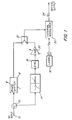
- FIG. 1 illustrates one embodiment of a predistortion circuit in accordance with the present invention.
- An RF input signal such as a cable television (“CATV”) signal is input at terminal 10.
- the signal is split into two paths at a conventional directional coupler 12.
- the phase of the signal is shifted by an adjustable phase shifter 16.
- the signal is distorted by a distortion generator 14 that can comprise a pair of diodes coupled with opposite polarities in parallel.
- the current-voltage characteristic of such a diode pair is illustrated within box 14.
- the distorted signal output from distortion generator 14 is input to an attenuator 18, and an adjustable gain amplifier 20.
- phase shifted signal from the first path and distorted signal from the second path are combined in a conventional coupler 22 to produce a modulation signal for external modulator 30.
- Modulator 30 which can be a Mach Zehnder modulator or other optical modulator, modulates a coherent light beam from a laser 32 for transmission over an optical fiber 34.
- the circuit illustrated in Figure 1 provides an adaptive harmonic distortion generator. It is designed to produce distortion components that are similar, but opposite in phase to those produced by external modulator 30. Phase shifter 16 and amplifier 20 are adjusted (e.g., by trial and error) to provide a phase delay and amplitude that result in an optimal linearization of the output from modulator 30. Amplifier 20 serves to set the level of distortion according to the modulation depth used to modulate optical modulator 30.
- distortion generator 14 does not have to be exactly the same as those produced by modulator 30.
- the only requirement on the distortion generator is to generate harmonic distortion components that have a similar order as those produced by the external modulator. Since external modulators generally introduce odd order harmonics, distortion generator 14 also generates odd order harmonics.
- FIG. 2 is a schematic diagram of a diode pair distortion generator that can be used in connection with the present invention.
- An input signal is coupled via terminal 40 to the anode of diode 44 and the cathode of diode 46.
- Resistor 42 provides a proper input impedance.
- Diode 46 is forward biased by a current source generally designated 80.
- the current source includes a conventional transistor pair 48, 50 with a potentiometer 60 to enable adjustment of the output current. Current is applied through a choke 56 that blocks AC components of the input signal from feeding back into the current source.
- a similar current source 82 is used to forward bias diode 44.
- This source includes transistor pair 52, 54 with potentiometer 62 that is used to adjust the output current.
- a choke 58 prevents AC components of the input signal from feeding back into the current source.
- Capacitors 64, 66 block the DC bias currents from feeding through with the distorted signal to output terminal 70.
- the output impedance of the circuit is established by resistor 68.
- Figure 3 is a simplified diagram of the circuit of Figure 2. Similarly numbered components provide the functions described above in connection with Figure 2.
- V o 2R L I B [V T V IN /(1+2V T I B (R S +R L )) +(V T V IN ) 3 /6(1+2V T I B (R S +R L )) 4 + ...]
- Figures 4a-4c are spectral responses, respectively, of signals passing through the distortion generator, external modulator, and the combined signals.
- an input signal with a frequency f 1 passes through the distortion generator with a spectral response 90.
- the distortion generator introduces a third order harmonic at 3 f 1 as shown at 96.
- the response of the external modulator, as indicated in Figure 4b, is such that the signal frequency f 1 passes with a response 92 in the same direction as the response 90 through the distortion generator.
- third order harmonics generated at 3 f 1 have a response 98 opposite in polarity to those introduced by the distortion generator.
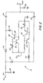
- FIG. 5 An alternate embodiment of a predistortion circuit in accordance with the present invention is illustrated in Figure 5.
- the RF input signal applied at terminal 110 is coupled to a directional coupler 112 that splits the signal into first and second paths.
- the signal is attenuated at a conventional attenuator 118 and passed to an adjustable phase shift circuit 116.
- the RF input signal is again split at a directional coupler 120.
- One output of coupler 120 couples the signal to a distortion generator 114 that can comprise the circuit illustrated in Figure 2.
- the phase shifted input signal from phase shifter 116 is subtracted at a combiner 122 from the distorted input signal from distortion generator 114.
- the output of combiner 122 contains the distortion components introduced by distortion generator 114.
- the distortion components output from combiner 122 are amplified by a variable gain, low noise linear amplifier 124 and summed in a summer 128 with the original RF input signal after amplification by another variable gain amplifier 126.
- the gains of amplifiers 124, 126 and the phase delay introduced by phase shifter 116 are set to optimize the linearization of an optical intensity modulator 130.
- the combined signal from summer 128 is used as a modulation signal for the modulator, which modulates an optical output signal from laser 132 for transmission on an optical fiber 134.
- the present invention provides a universal predistortion circuit that is useful in linearizing the output of an optical intensity modulator.
- the circuit is useful in broadband multi-channel transmission systems, such as CATV distribution systems.
- the use of a predistorted modulation signal in conjunction with a conventional optical intensity modulator effectively reduces the third order nonlinearity generated by the modulator. As a result, a higher optical modulation index can be used resulting in a higher link power budget for a given source of optical power.
- the phase delay and amplitude of the modulating signal By adjusting the phase delay and amplitude of the modulating signal, the intrinsic third order composite triple beats of the modulator are reduced.
Claims (20)
- Dispositif pour fournir un signal préalablement déformé à utiliser pour linéariser un modulateur d'intensité optique externe (30, 130), comprenant :des moyens pour séparer (12, 112) un signal d'entrée en des premier et second trajets,des moyens de production de distorsion (14, 114) raccordés au second trajet afin d'introduire des composantes de distorsion dans le signal d'entrée,des moyens de décalage de phase (16, 116) raccordés à un des trajets pour décaler, dans le premier trajet, la phase du signal d'entrée par rapport au signal d'entrée déformé du second trajet, etdes moyens pour combiner (22, 122) le signal d'entrée en provenance du premier trajet et le signal d'entrée déformé du second trajet afin de former un signal combiné pour fournir le signal préalablement déformé en vue de moduler un signal de sortie sortie d'une source lumineuse par le modulateur d'intensité optique externe.
- Dispositif suivant la revendication 1, caractérisé en ce que les moyens de production de distorsion (14, 114) comprennent :une paire de diodes (44, 46) raccordées en parallèle avec des polarités opposées,une première source de courant (80) pour polariser en sens direct une des diodes,une seconde source de courant (82) pour polariser en sens direct l'autre des diodes, etdes moyens pour raccorder la paire de diodes (44, 46) en série avec le second trajet.
- Dispositif suivant la revendication 1 ou 2, caractérisé en ce que les moyens de décalage de phase (16, 116) sont réglables pour fournir un retard de phase souhaité.
- Dispositif suivant l'une quelconque des revendications 1 à 3, caractérisé en ce qu'il comprend en outre :
un amplificateur à gain variable (20, 124) raccordé pour amplifier de façon réglable les composantes de distorsion. - Dispositif suivant la revendication 4, caractérisé en ce que l'amplificateur à gain variable (20) est raccordé dans le second trajet, entre les moyens de production de distorsion (14) et les moyens de combinaison (22).
- Dispositif suivant la revendication 4 ou 5, caractérisé en ce qu'il comprend en outre :
un atténuateur (18) raccordé entre les moyens de production de distorsion (14) et l'amplificateur (20). - Dispositif suivant l'une quelconque des revendications 4 à 6, caractérisé en ce que l'amplificateur à gain variable (124) est raccordé pour amplifier le signal combiné fourni par les moyens de combinaison (122).
- Dispositif suivant l'une quelconque des revendications précédentes, caractérisé en ce que les moyens de combinaison (122) soustraient le signal d'entrée décalé en phase du signal d'entrée déformé afin de fournir le signal combiné qui comprend à la base les composantes de distorsion.
- Dispositif suivant l'une quelconque des revendications précédentes, caractérisé en ce qu'il comprend :
des moyens pour ajouter (128) le signal d'entrée et le signal combiné en provenance des moyens de combinaison (122) afin de procurer le signal préalablement déformé précité pour le modulateur d'intensité optique externe (30, 130). - Dispositif suivant la revendication 9, caractérisé en ce qu'il comprend en outre :
des moyens d'amplification (126) pour amplifier le signal d'entrée avant de l'ajouter aux composantes de distorsion précitées. - Dispositif suivant l'une quelconque des revendications précédentes, caractérisé en ce que la source de lumière est un laser à solide (32, 132).
- Dispositif suivant l'une quelconque des revendications précédentes, caractérisé en ce que le signal préalablement déformé est raccordé à un modulateur de Mach Zehnder (30, 130) destiné à moduler un signal de sortie du laser (32, 132).
- Dispositif suivant l'une quelconque des revendications précédentes, caractérisé en ce que les moyens de production de distorsion (14, 114) procurent des composantes de distorsion d'ordre impair.
- Dispositif suivant l'une quelconque des revendications 4 à 13, caractérisé en ce qu'il comprend :des moyens pour régler le gain de l'amplificateur (20, 126) afin de fournir les composantes de distorsion à un niveau nécessaire pour linéariser le signal de sortie du modulateur (30, 130), etdes moyens pour raccorder (22, 126) les composantes de distorsion amplifiées à une entrée de signal modulant du modulateur (30, 130) précité.
- Dispositif suivant l'une quelconque des revendications précédentes, caractérisé en ce que les moyens de décalage de phase (16, 116) décalent la phase du signal d'entrée afin de compenser un décalage de phase introduit par les moyens de distorsion (14, 114).
- Dispositif suivant la revendication 14 ou 15, caractérisé en ce que les composantes de distorsion sont des composantes de distorsion d'ordre impair semblables mais opposées en polarité à des composantes de distorsion introduites par le modulateur (30, 130).
- Dispositif suivant l'une quelconque des revendications précédentes, caractérisé en ce que les moyens de décalage de phase (16, 116) sont raccordés au premier trajet.
- Procédé pour linéariser le signal de sortie d'un modulateur optique analogique externe (30, 130), comprenant les étapes de :dédoubler un signal d'entrée en des premier et second trajets,déformer le signal d'entrée dans le second trajet,régler la phase du signal d'entrée, dans le premier trajet, par rapport au signal d'entrée du second trajet afin de compenser un décalage de phase introduit dans le signal d'entrée déformé du second trajet, etcombiner le signal d'entrée en provenance du premier trajet et le signal d'entrée déformé en provenance du second trajet afin de former un signal combiné pour fournir un signal préalablement déformé.
- Procédé suivant la revendication 18, caractérisé en ce qu'il comprend les étapes de :
déformer le signal d'entrée du second trajet avec des composantes de distorsion d'ordre impair semblables mais opposées en polarité à des composantes de distorsion introduites par le modulateur (30, 130) précité. - Procédé suivant la revendication 18 ou 19, caractérisé en ce qu'il comprend en outre les étapes de :
amplifier de façon variable dans le second trajet le signal d'entrée déformé.
Applications Claiming Priority (2)
| Application Number | Priority Date | Filing Date | Title |
|---|---|---|---|
| US581015 | 1984-02-17 | ||
| US07/581,015 US5210633A (en) | 1990-09-12 | 1990-09-12 | Apparatus and method for linearizing the operation of an external optical modulator |
Publications (3)
| Publication Number | Publication Date |
|---|---|
| EP0475376A2 EP0475376A2 (fr) | 1992-03-18 |
| EP0475376A3 EP0475376A3 (en) | 1992-12-09 |
| EP0475376B1 true EP0475376B1 (fr) | 1997-03-12 |
Family
ID=24323563
Family Applications (1)
| Application Number | Title | Priority Date | Filing Date |
|---|---|---|---|
| EP91115326A Expired - Lifetime EP0475376B1 (fr) | 1990-09-12 | 1991-09-11 | Dispositif et procédé de linéarisation du fonctionnement d'un modulateur optique externe |
Country Status (8)
| Country | Link |
|---|---|
| US (1) | US5210633A (fr) |
| EP (1) | EP0475376B1 (fr) |
| JP (1) | JPH06342178A (fr) |
| CA (1) | CA2051227C (fr) |
| DE (1) | DE69125075T2 (fr) |
| HK (1) | HK1008408A1 (fr) |
| MX (1) | MX9101051A (fr) |
| NO (1) | NO306081B1 (fr) |
Families Citing this family (46)
| Publication number | Priority date | Publication date | Assignee | Title |
|---|---|---|---|---|
| US5252930A (en) * | 1989-09-07 | 1993-10-12 | Ortel Corporation | Predistorter for linearization of electronic and optical signals |
| US5361156A (en) * | 1991-12-09 | 1994-11-01 | Scientific-Atlanta, Inc. | Method and apparatus for predistortion |
| FR2688365B1 (fr) * | 1992-03-09 | 1994-04-29 | France Telecom | Procede de transmission optique d'un multiplex de porteuses electriques et dispositif pour la mise en óoeuvre de ce procede. |
| US5430569A (en) * | 1992-05-22 | 1995-07-04 | Ortel Corporation | Suppression of noise and distortion in fiber-optic systems |
| US5327279A (en) * | 1992-07-17 | 1994-07-05 | United Technologies Corporation | Apparatus for linearization of optic modulators using a feed-forward predistortion circuit |
| CA2141560C (fr) * | 1992-08-06 | 2004-06-29 | Erich Gottwald | Methode et circuit pour corriger la distorsion causee dans les signaux par les glissements de frequence laser et la dispersion dans les fibres |
| DE4234599A1 (de) * | 1992-08-22 | 1994-02-24 | Sel Alcatel Ag | Optischer Sender |
| SG52501A1 (en) * | 1992-10-21 | 1998-09-28 | At & T Corp | Cascaded distortion compensation for analog optical systems |
| US5420711A (en) * | 1993-01-19 | 1995-05-30 | Snyder; Dan E. | Fiber optic link amplitude stabilization circuit |
| SE501070C2 (sv) * | 1993-03-26 | 1994-11-07 | Ericsson Telefon Ab L M | System och förfarande för dispersionskompensering i fiberoptiska höghastighetssystem |
| SE501932C2 (sv) * | 1993-04-30 | 1995-06-26 | Ericsson Telefon Ab L M | Anordning och förfarande för dispersionskompensering i ett fiberoptiskt transmissionssystem |
| US5600473A (en) * | 1993-06-04 | 1997-02-04 | Ciena Corporation | Optical amplifier systems with add/drop multiplexing |
| US5579143A (en) * | 1993-06-04 | 1996-11-26 | Ciena Corporation | Optical system with tunable in-fiber gratings |
| DE4342184A1 (de) * | 1993-12-10 | 1995-06-14 | Sel Alcatel Ag | Optischer Sender mit linearisierendem Netzwerk |
| JP2697639B2 (ja) * | 1994-11-04 | 1998-01-14 | 日本電気株式会社 | 光変調装置 |
| US5710653A (en) * | 1995-03-06 | 1998-01-20 | Fiber Optic Network Solutions Corp. | Linear multi-output optical transmitter system |
| US5875048A (en) * | 1995-03-06 | 1999-02-23 | Cfx Communication Systems,Llc | Linear multi-output optical transmitter system |
| US5699179A (en) * | 1996-02-23 | 1997-12-16 | General Instrument Corporation Of Delaware | Cancellation of distortion components in a fiber optic link with feed-forward linearization |
| US5953139A (en) * | 1996-03-06 | 1999-09-14 | Cfx Communications Systems, Llc | Wavelength division multiplexing system |
| US5850305A (en) * | 1996-12-18 | 1998-12-15 | Scientific-Atlanta, Inc. | Adaptive predistortion control for optical external modulation |
| AU744572B2 (en) * | 1997-05-12 | 2002-02-28 | Corning O.T.I Inc. | External optical modulation system comprising a predistorter |
| TW336363B (en) * | 1997-06-20 | 1998-07-11 | New Elite Technologies Inc | Distortion compensation device for broadband fiber optic transmission system |
| US5915052A (en) * | 1997-06-30 | 1999-06-22 | Uniphase Telecommunications Products, Inc. | Loop status monitor for determining the amplitude of the signal components of a multi-wavelength optical beam |
| US5982964A (en) * | 1997-06-30 | 1999-11-09 | Uniphase Corporation | Process for fabrication and independent tuning of multiple integrated optical directional couplers on a single substrate |
| US6151157A (en) * | 1997-06-30 | 2000-11-21 | Uniphase Telecommunications Products, Inc. | Dynamic optical amplifier |
| US6370290B1 (en) | 1997-09-19 | 2002-04-09 | Uniphase Corporation | Integrated wavelength-select transmitter |
| US6031849A (en) * | 1997-11-14 | 2000-02-29 | Jds Uniphase Corporation | High power three level fiber laser and method of making same |
| US6020986A (en) * | 1997-11-21 | 2000-02-01 | Jds Uniphase Corporation | Programmable add-drop module for use in an optical circuit |
| EP0926847A1 (fr) * | 1997-12-23 | 1999-06-30 | PIRELLI CAVI E SISTEMI S.p.A. | Système de modulation optique externe comprenant un dispositif de prédistortion |
| US6198419B1 (en) * | 1998-06-17 | 2001-03-06 | Lucent Technologies, Inc. | Method and apparatus for extending the spurious free dynamic range of a digital-to-analog converter |
| DE19831715A1 (de) | 1998-07-15 | 2000-01-20 | Alcatel Sa | Arbeitspunkteinstellung einer Diode eines Diodennetzwerkes durch Spannungseinprägung |
| DE19831717A1 (de) | 1998-07-15 | 2000-01-20 | Alcatel Sa | Temperaturstabilisation eines Predistorters |
| DE19831716A1 (de) | 1998-07-15 | 2000-01-20 | Alcatel Sa | Temperaturstabilisation eines Predistorters mit Spannungsspeisung |
| US6310990B1 (en) | 2000-03-16 | 2001-10-30 | Cidra Corporation | Tunable optical structure featuring feedback control |
| JP2000244252A (ja) * | 1999-02-24 | 2000-09-08 | Kokusai Electric Co Ltd | 歪み補償装置 |
| JP2003518641A (ja) * | 1999-12-24 | 2003-06-10 | コーニング オーティーアイ インコーポレイテッド | アナログ変調の方法及びこの方法を用いる光エミッタ |
| WO2001050643A1 (fr) * | 2000-01-06 | 2001-07-12 | Adc Telecommunications, Inc. | Dispositif de predistorsion comportant des elements non magnetiques pour dispositif non lineaire |
| US6687466B1 (en) | 2000-01-06 | 2004-02-03 | Adc Telecommunications, Inc. | Dynamic distortion control |
| US6707402B1 (en) | 2000-02-11 | 2004-03-16 | Georg Neumann Gmbh | Method for converting an analog signal to a digital signal |
| GB2372830B (en) * | 2001-03-02 | 2003-05-21 | Marconi Caswell Ltd | Electro-optic gating arrangement with improved duty cycle |
| CN100499357C (zh) * | 2004-10-28 | 2009-06-10 | 三菱电机株式会社 | 线性化电路 |
| GB2428149B (en) * | 2005-07-07 | 2009-10-28 | Agilent Technologies Inc | Multimode optical fibre communication system |
| GB2442773A (en) * | 2006-10-11 | 2008-04-16 | Tandberg Television Asa | Canceling distortion |
| US7945172B2 (en) * | 2008-05-20 | 2011-05-17 | Harmonic, Inc. | Dispersion compensation circuitry and system for analog video transmission with direct modulated laser |
| CN109856477B (zh) * | 2018-12-24 | 2021-08-10 | 中国信息通信研究院 | 一种激励射频有源器件的方法及输入优化测试系统 |
| US11914263B2 (en) * | 2019-03-14 | 2024-02-27 | The Regents Of The University Of California | Analog predistortion linearization for optical fiber communication links |
Family Cites Families (14)
| Publication number | Priority date | Publication date | Assignee | Title |
|---|---|---|---|---|
| JPS5851435B2 (ja) * | 1976-05-25 | 1983-11-16 | 富士通株式会社 | 発光素子の駆動方式 |
| US4075474A (en) * | 1977-04-19 | 1978-02-21 | Northern Telecom Limited | Method and apparatus for distortion reduction in optical communication systems |
| EP0037857B1 (fr) * | 1980-04-14 | 1985-01-23 | ATELIERS DE CONSTRUCTIONS ELECTRIQUES DE CHARLEROI (ACEC) Société Anonyme | Procédé de transmission d'information analogique à travers des fibres optiques et installation pour le réaliser |
| DE3142203A1 (de) * | 1981-10-24 | 1983-05-26 | AEG-Telefunken Nachrichtentechnik GmbH, 7150 Backnang | Entzerrer |
| JPS60142630A (ja) * | 1983-12-28 | 1985-07-27 | Fujitsu Ltd | 伝搬歪補償装置 |
| US4715021A (en) * | 1984-08-08 | 1987-12-22 | Exxon Production Research Co. | Method for filtering and combining seismic data having different spectral characteristics |
| US4699466A (en) * | 1985-03-27 | 1987-10-13 | Grumman Aerospace Corporation | Optical RF filtering system |
| US4588958A (en) * | 1985-03-29 | 1986-05-13 | Rca Corporation | Adjustable reflective predistortion circuit |
| GB8602017D0 (en) * | 1986-01-28 | 1986-03-05 | British Telecomm | Reducing fluctuations in radiation beam characteristic |
| US4752743A (en) * | 1986-09-26 | 1988-06-21 | Varian Associates, Inc. | Linearizer for TWT amplifiers |
| JP2610667B2 (ja) * | 1988-11-25 | 1997-05-14 | 住友電気工業株式会社 | 光通信システム |
| US5031235A (en) * | 1989-10-27 | 1991-07-09 | Hoechst Celanese Corp. | Cable system incorporating highly linear optical modulator |
| US5003624A (en) * | 1990-03-29 | 1991-03-26 | Hughes Aircraft Company | Automatic bias controller for electro-optic modulator |
| US5012475A (en) * | 1990-04-17 | 1991-04-30 | Wavelength Lasers, Inc. | Analog compensation system for linear lasers |
-
1990
- 1990-09-12 US US07/581,015 patent/US5210633A/en not_active Expired - Lifetime
-
1991
- 1991-09-11 EP EP91115326A patent/EP0475376B1/fr not_active Expired - Lifetime
- 1991-09-11 MX MX9101051A patent/MX9101051A/es unknown
- 1991-09-11 DE DE69125075T patent/DE69125075T2/de not_active Expired - Fee Related
- 1991-09-11 NO NO913576A patent/NO306081B1/no unknown
- 1991-09-12 JP JP3260449A patent/JPH06342178A/ja not_active Withdrawn
- 1991-09-12 CA CA002051227A patent/CA2051227C/fr not_active Expired - Fee Related
-
1998
- 1998-06-24 HK HK98106360A patent/HK1008408A1/xx not_active IP Right Cessation
Also Published As
| Publication number | Publication date |
|---|---|
| DE69125075D1 (de) | 1997-04-17 |
| MX9101051A (es) | 1992-05-04 |
| HK1008408A1 (en) | 1999-05-07 |
| NO913576L (no) | 1992-03-13 |
| NO913576D0 (no) | 1991-09-11 |
| JPH06342178A (ja) | 1994-12-13 |
| DE69125075T2 (de) | 1997-09-11 |
| NO306081B1 (no) | 1999-09-13 |
| EP0475376A3 (en) | 1992-12-09 |
| CA2051227A1 (fr) | 1992-03-13 |
| US5210633A (en) | 1993-05-11 |
| EP0475376A2 (fr) | 1992-03-18 |
| CA2051227C (fr) | 2000-08-15 |
Similar Documents
| Publication | Publication Date | Title |
|---|---|---|
| EP0475376B1 (fr) | Dispositif et procédé de linéarisation du fonctionnement d'un modulateur optique externe | |
| US5963352A (en) | Linearization enhanced operation of single-stage and dual-stage electro-optic modulators | |
| US5436749A (en) | Method and apparatus for predistortion | |
| EP0416622B1 (fr) | Dispositif de prédistorsion pour la linéarisation de signaux électroniques et optiques | |
| US5481389A (en) | Postdistortion circuit for reducing distortion in an optical communications system | |
| US5850305A (en) | Adaptive predistortion control for optical external modulation | |
| US4893300A (en) | Technique for reducing distortion characteristics in fiber-optic links | |
| US5359450A (en) | Optical transmission system | |
| US6232836B1 (en) | In-line, unbalanced amplifier, predistortion circuit | |
| CA2211923C (fr) | Systeme optique a traitement quasi-incoherent pour la correction des distorsions | |
| US5227736A (en) | Second-order predistorter | |
| EP0768765B1 (fr) | Système de réglage de la tension de polarisation d'un modulateur optique pour CATV | |
| USRE44647E1 (en) | Directly modulated laser optical transmission system with phase modulation | |
| US6917764B1 (en) | Predistortion circuit with combined odd-order and even-order correction | |
| US5428314A (en) | Odd/even order distortion generator and distortion cancellation circuit | |
| US6619866B1 (en) | Dynamic range extended for optical transmitters | |
| EP1249086B1 (fr) | Dispositif de predistorsion comportant des elements non magnetiques pour dispositif non lineaire | |
| Alameh et al. | Optimization of fiber amplifier SCM lightwave video systems using direct and external modulation | |
| JPH03104331A (ja) | アナログ光通信システムにおけるひずみ減少装置と方式 | |
| Ismail et al. | Nonlinear distortion reduction in directly modulated semiconductor laser using feedforward linearisation | |
| Young et al. | High dynamic range analog optical modulator | |
| CN114978330A (zh) | 一种前馈后补偿线性化射频光发射机及其改善方法 | |
| Ellis et al. | Feedback control of a linearised Mach-Zehnder modulator for SCM applications | |
| Lin et al. | A predistortion technique for multichannel AM-VSB lightwave CATV systems | |
| Yang et al. | Design of a high-power highly linear directly modulated 1.3-um DFB laser transmitter for multichannel CATV transmissions |
Legal Events
| Date | Code | Title | Description |
|---|---|---|---|
| PUAI | Public reference made under article 153(3) epc to a published international application that has entered the european phase |
Free format text: ORIGINAL CODE: 0009012 |
|
| AK | Designated contracting states |
Kind code of ref document: A2 Designated state(s): BE CH DE FR GB IT LI NL SE |
|
| PUAL | Search report despatched |
Free format text: ORIGINAL CODE: 0009013 |
|
| AK | Designated contracting states |
Kind code of ref document: A3 Designated state(s): BE CH DE FR GB IT LI NL SE |
|
| 17P | Request for examination filed |
Effective date: 19930227 |
|
| RAP1 | Party data changed (applicant data changed or rights of an application transferred) |
Owner name: GI CORPORATION |
|
| RAP1 | Party data changed (applicant data changed or rights of an application transferred) |
Owner name: GENERAL INSTRUMENT CORPORATION OF DELAWARE |
|
| 17Q | First examination report despatched |
Effective date: 19950509 |
|
| GRAG | Despatch of communication of intention to grant |
Free format text: ORIGINAL CODE: EPIDOS AGRA |
|
| GRAH | Despatch of communication of intention to grant a patent |
Free format text: ORIGINAL CODE: EPIDOS IGRA |
|
| GRAH | Despatch of communication of intention to grant a patent |
Free format text: ORIGINAL CODE: EPIDOS IGRA |
|
| GRAH | Despatch of communication of intention to grant a patent |
Free format text: ORIGINAL CODE: EPIDOS IGRA |
|
| GRAH | Despatch of communication of intention to grant a patent |
Free format text: ORIGINAL CODE: EPIDOS IGRA |
|
| GRAA | (expected) grant |
Free format text: ORIGINAL CODE: 0009210 |
|
| AK | Designated contracting states |
Kind code of ref document: B1 Designated state(s): BE CH DE FR GB IT LI NL SE |
|
| ITF | It: translation for a ep patent filed |
Owner name: 0403;01MIFBARZANO' E ZANARDO MILANO S.P. |
|
| REG | Reference to a national code |
Ref country code: CH Ref legal event code: EP Ref country code: CH Ref legal event code: NV Representative=s name: KIRKER & CIE SA |
|
| REF | Corresponds to: |
Ref document number: 69125075 Country of ref document: DE Date of ref document: 19970417 |
|
| ET | Fr: translation filed | ||
| PLBE | No opposition filed within time limit |
Free format text: ORIGINAL CODE: 0009261 |
|
| STAA | Information on the status of an ep patent application or granted ep patent |
Free format text: STATUS: NO OPPOSITION FILED WITHIN TIME LIMIT |
|
| 26N | No opposition filed | ||
| REG | Reference to a national code |
Ref country code: GB Ref legal event code: 732E |
|
| REG | Reference to a national code |
Ref country code: GB Ref legal event code: IF02 |
|
| PGFP | Annual fee paid to national office [announced via postgrant information from national office to epo] |
Ref country code: NL Payment date: 20040809 Year of fee payment: 14 |
|
| PGFP | Annual fee paid to national office [announced via postgrant information from national office to epo] |
Ref country code: SE Payment date: 20040903 Year of fee payment: 14 |
|
| PGFP | Annual fee paid to national office [announced via postgrant information from national office to epo] |
Ref country code: CH Payment date: 20040914 Year of fee payment: 14 |
|
| PGFP | Annual fee paid to national office [announced via postgrant information from national office to epo] |
Ref country code: BE Payment date: 20040928 Year of fee payment: 14 |
|
| PGFP | Annual fee paid to national office [announced via postgrant information from national office to epo] |
Ref country code: GB Payment date: 20050809 Year of fee payment: 15 |
|
| PGFP | Annual fee paid to national office [announced via postgrant information from national office to epo] |
Ref country code: FR Payment date: 20050902 Year of fee payment: 15 |
|
| PG25 | Lapsed in a contracting state [announced via postgrant information from national office to epo] |
Ref country code: IT Free format text: LAPSE BECAUSE OF NON-PAYMENT OF DUE FEES Effective date: 20050911 |
|
| PG25 | Lapsed in a contracting state [announced via postgrant information from national office to epo] |
Ref country code: SE Free format text: LAPSE BECAUSE OF NON-PAYMENT OF DUE FEES Effective date: 20050912 |
|
| PG25 | Lapsed in a contracting state [announced via postgrant information from national office to epo] |
Ref country code: CH Free format text: LAPSE BECAUSE OF NON-PAYMENT OF DUE FEES Effective date: 20050930 Ref country code: BE Free format text: LAPSE BECAUSE OF NON-PAYMENT OF DUE FEES Effective date: 20050930 Ref country code: LI Free format text: LAPSE BECAUSE OF NON-PAYMENT OF DUE FEES Effective date: 20050930 |
|
| PGFP | Annual fee paid to national office [announced via postgrant information from national office to epo] |
Ref country code: DE Payment date: 20050930 Year of fee payment: 15 |
|
| PG25 | Lapsed in a contracting state [announced via postgrant information from national office to epo] |
Ref country code: NL Free format text: LAPSE BECAUSE OF NON-PAYMENT OF DUE FEES Effective date: 20060401 |
|
| REG | Reference to a national code |
Ref country code: CH Ref legal event code: PL |
|
| EUG | Se: european patent has lapsed | ||
| NLV4 | Nl: lapsed or anulled due to non-payment of the annual fee |
Effective date: 20060401 |
|
| PG25 | Lapsed in a contracting state [announced via postgrant information from national office to epo] |
Ref country code: DE Free format text: LAPSE BECAUSE OF NON-PAYMENT OF DUE FEES Effective date: 20070403 |
|
| GBPC | Gb: european patent ceased through non-payment of renewal fee |
Effective date: 20060911 |
|
| REG | Reference to a national code |
Ref country code: FR Ref legal event code: ST Effective date: 20070531 |
|
| PG25 | Lapsed in a contracting state [announced via postgrant information from national office to epo] |
Ref country code: GB Free format text: LAPSE BECAUSE OF NON-PAYMENT OF DUE FEES Effective date: 20060911 |
|
| BERE | Be: lapsed |
Owner name: *GENERAL INSTRUMENT CORP. OF DELAWARE Effective date: 20050930 |
|
| PG25 | Lapsed in a contracting state [announced via postgrant information from national office to epo] |
Ref country code: FR Free format text: LAPSE BECAUSE OF NON-PAYMENT OF DUE FEES Effective date: 20061002 |
|
| P01 | Opt-out of the competence of the unified patent court (upc) registered |
Effective date: 20230520 |