EP0474584A2 - Source de plasma radiofréquence à couplage capacitif - Google Patents
Source de plasma radiofréquence à couplage capacitif Download PDFInfo
- Publication number
- EP0474584A2 EP0474584A2 EP91630060A EP91630060A EP0474584A2 EP 0474584 A2 EP0474584 A2 EP 0474584A2 EP 91630060 A EP91630060 A EP 91630060A EP 91630060 A EP91630060 A EP 91630060A EP 0474584 A2 EP0474584 A2 EP 0474584A2
- Authority
- EP
- European Patent Office
- Prior art keywords
- plasma
- electrode
- source
- plasma source
- magnetic field
- Prior art date
- Legal status (The legal status is an assumption and is not a legal conclusion. Google has not performed a legal analysis and makes no representation as to the accuracy of the status listed.)
- Granted
Links
Images
Classifications
-
- H—ELECTRICITY
- H01—ELECTRIC ELEMENTS
- H01J—ELECTRIC DISCHARGE TUBES OR DISCHARGE LAMPS
- H01J27/00—Ion beam tubes
- H01J27/02—Ion sources; Ion guns
- H01J27/16—Ion sources; Ion guns using high-frequency excitation, e.g. microwave excitation
- H01J27/18—Ion sources; Ion guns using high-frequency excitation, e.g. microwave excitation with an applied axial magnetic field
-
- H—ELECTRICITY
- H01—ELECTRIC ELEMENTS
- H01J—ELECTRIC DISCHARGE TUBES OR DISCHARGE LAMPS
- H01J37/00—Discharge tubes with provision for introducing objects or material to be exposed to the discharge, e.g. for the purpose of examination or processing thereof
- H01J37/32—Gas-filled discharge tubes
- H01J37/32009—Arrangements for generation of plasma specially adapted for examination or treatment of objects, e.g. plasma sources
- H01J37/32082—Radio frequency generated discharge
- H01J37/32091—Radio frequency generated discharge the radio frequency energy being capacitively coupled to the plasma
-
- H—ELECTRICITY
- H01—ELECTRIC ELEMENTS
- H01J—ELECTRIC DISCHARGE TUBES OR DISCHARGE LAMPS
- H01J37/00—Discharge tubes with provision for introducing objects or material to be exposed to the discharge, e.g. for the purpose of examination or processing thereof
- H01J37/32—Gas-filled discharge tubes
- H01J37/32009—Arrangements for generation of plasma specially adapted for examination or treatment of objects, e.g. plasma sources
- H01J37/32357—Generation remote from the workpiece, e.g. down-stream
-
- H—ELECTRICITY
- H01—ELECTRIC ELEMENTS
- H01J—ELECTRIC DISCHARGE TUBES OR DISCHARGE LAMPS
- H01J37/00—Discharge tubes with provision for introducing objects or material to be exposed to the discharge, e.g. for the purpose of examination or processing thereof
- H01J37/32—Gas-filled discharge tubes
- H01J37/32431—Constructional details of the reactor
- H01J37/3266—Magnetic control means
- H01J37/32688—Multi-cusp fields
-
- H—ELECTRICITY
- H05—ELECTRIC TECHNIQUES NOT OTHERWISE PROVIDED FOR
- H05H—PLASMA TECHNIQUE; PRODUCTION OF ACCELERATED ELECTRICALLY-CHARGED PARTICLES OR OF NEUTRONS; PRODUCTION OR ACCELERATION OF NEUTRAL MOLECULAR OR ATOMIC BEAMS
- H05H1/00—Generating plasma; Handling plasma
- H05H1/24—Generating plasma
- H05H1/46—Generating plasma using applied electromagnetic fields, e.g. high frequency or microwave energy
Definitions
- This invention relates to plasma sources. More particularly, it pertains to a plasma source in which radiofrequency energy is capacitively coupled to a discharge process in order to generate a plasma having ions and electrons.
- Broad-beam ion sources in which grids with a plurality of apertures serve to electrostatically accelerate ions have been used for many years both for electric space propulsion and in industrial applications.
- a review of the history and technology was presented by H.R. Kaufman in "Broad-Beam Ion Sources", Review of Scientific Instruments , Vol. 61, pp.230-235, Jan. 1990.
- the ion-generating discharges most often have been of the direct-current (dc) type.
- An electron-emitting cathode is a critical component for a dc discharge by reason of either adding complexity by requiring a special electron source such as a hollow cathode or by exhibiting only the limited lifetime typical of a hot filament.
- Radiofrequency (RF) energy can be used to generate ions using either inductive or capacitive coupling to deliver the RF energy to the plasma.
- inductive coupling is illustrated in U.S. patent No. 3,903,891 issued September 9, 1975 to Brayshaw.
- U.S. patent No. 4,479,075 issued October 23, 1984 to Elliot describes the use of capacitive coupling as does an article by K. Kohler, J.W. Coburn, D.E. Horne, E. Kay and J.H. Keller, "Plasma Potentials of 13.56-MHz RF Argon Glow Discharges in a Planar System", Journal of Applied Physics , Vol. 57, pp. 59-66, Jan. 1985.
- the use of an RF discharge process thus offers a means of avoiding cathode limitations and problems.
- ion sources incorporating RF discharges have had other problems.
- an inductively coupled RF process has been utilized in an ion source by placing a dielectric window between the inductor and the discharge region as shown by Birner et al. in U.S. patent 4,104,875, issued August 8, 1978.
- a dielectric window is sensitive to conductive deposits that can easily result from sputtering. When a dielectric window becomes coated with such deposits, the RF energy can no longer reach the discharge region. Such sensitivity is undesirable in industrial applications where a variety of contaminates is encountered. If the dielectric window is omitted, on the other hand, the inductor is exposed directly to the plasma as a result of which cooling the inductor can become a problem. Because the discharge chamber is normally at an elevated potential, internal liquid cooling of such an inductor requires either voltage isolation or the operation of a cooling system at an elevated potential.
- capacitively-coupled RF discharge processes have also been used in ion sources. However, they require the development of a magnetic field in order to reach a normal operating pressure of less than one milliTorr (approximately less than 0.1 Pascal).
- RF diode which uses a capacitively-coupled RF energy and in which a plasma is developed as discussed by H.R. Kaufman and S.M. Rossnagel in "Analysis of Area-Ratio Effect for Radio-Frequency Diode", J. of Vacuum Science and Technology A , Vol. A6, pp.2572-2573. July/Aug. 1988.
- the RF diode has been widely used, it is relatively well understood and it has some basic similarities to apparatus in accordance with the present invention. In contrast, however, it has no magnetic field, normally operates at twenty-thirty milliTorr and has a minimum peak-to-peak voltage between electrodes of about two-hundred volts.
- the voltage level in the RF diode is sufficiently high to generate considerable internal sputtering that may result in contamination of a target which is etched, serves as a sputter source for disposition elsewhere or on which a film is being deposited and the particle beam results in property modification or enhancement compared to a film that is deposited without bombardment. Because of its degree of similarity, further discussion of the RF diode is set forth below.
- a general object of the present invention is to provide a new and improved radiofrequency-energy-driven plasma source.
- Another object of the present invention is to provide a novel plasma source which avoids the disadvantages and undesirable features of such prior plasma sources as those hereinbefore discussed.
- a further object of the present invention is to provide a novel plasma source which produces charged particles that may be accelerated in more than one way as for example but without limitation electrostatically through the use of apertured grids, electromagnetically as happens in an end-Hall ion source, or otherwise.
- Yet another object of the present invention is to provide a novel plasma source which produces low-energy changed particles that may be used for ion-beam neutralization (electrons) or low-energy bombardment of a surface (ions).
- a still further object of the present invention is to provide a novel RF plasma source useful in both space propulsion and in connection with industrial applications.
- a more specific object of the present invention is to provide a new plasma source which involves an improved manner of enhancing energy transfer from an RF electrode surface to a low pressure plasma.
- Still another object of the present invention is to provide a new and improved plasma source in which energetic electrons are contained as a part of the operative combination.
- Yet another object of the present invention is to provide a novel RF driven plasma source with an arrangement that reduces the plasma sheath voltages to a low level in order to reduce sputtering.
- One more detailed object of the present invention is to provide a novel RF-driven plasma source wherein reduced target contamination is obtained by arrangement of the source so that an RF-driven electrode is removed from direct view of the target.
- a plasma source is operative within an evacuated environment into which an ionizable gas is introduced.
- a first electrode is spaced from plasma discharge region within the source.
- a field producer develops a magnetic field oriented in a direction substantially parallel to the electrode surface area in enhancement of the transfer of the energy to the plasma.
- the second electrode surface area is of a size significantly smaller than the size of the surface area of the first electrode.
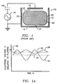
- a typical RF diode 10 represents a capacitively-coupled RF plasma source such as disclosed in the aforementioned Kohler et al. reference.
- the diode elements are a grounded electrode 12 having a cup shape and a driven or excitation-electrode 14 having the shape of a flat disc mounted in the open side of electrode 12.
- a radiofrequency source or supply 16 is coupled across electrodes 12 and 14 through a dc-isolating capacitor 18.
- a plasma 20 is produced within the inner region bounded by electrodes 12 and 14.
- Plasma 20 is separated from the wall of larger electrode 12 by a plasma sheath 22 as well as being separated from smaller electrode 14 by a plasma sheath 24.
- the potential 32 on excitation electrode 14 also follows an approximately sinusoidal variation with time but its waveform is displaced one-hundredand eighty degrees from the potential wave-form of electrode 12.
- the average potential value 34 is also negative relative to plasma potential 26 so that the peak value of potential 32 also is approximately equal to plasma potential 26.
- That the peak potential for each electrode is approximately equal to that of the plasma is a result of the high mobility of electrons relative to that of ions.
- the net current to each electrode must equal zero, and a very short period of electron conduction during each RF cycle is sufficient to supply a number of electrons equal to the number of ions that arrive at those electrodes during the rest of the cycle.
- the impedences of sheaths 22 and 24 are essentially capacitive which results in an inverse relationship between electrode areas and the amplitudes of the RF potential variations on those electrodes.
- the potential variations of the two electrodes should be about equal.
- the potential variation is greatest at the small electrode as indicated in Figure 1a.
- the exponent of that inverse variation as between potential variation and electrode areas depends on the relationship between the average potential difference across a plasma sheath and the ion arrival rate at that sheath. A more detailed explanation of that relationship may be had by reference to H.R. Kaufman and S.M. Rossnagel, "Analysis of Area-Ratio Effect for Radio-Frequency Diode", J. of Vacuum Science and Technology A , Vol. A6, pp. 2572-2573, July/Aug. 1988.
- Such an RF diode operates with no magnetic field. As mentioned in the introduction, it normally operates at twenty-thirty milliTorr and has a minimum peak-to-peak voltage between electrodes of about two-hundred volts. In addition to an excessively high pressure for use in a broad-beam charged-particle source, such a voltage level is high enough to generate considerable internal sputtering with the result of contamination of any target impinged upon by the charged-particle beam.
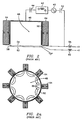
- a radiofrequency power source or supply 40 is coupled through a tuning network 42 and capacitor 44 to a driven electrode 46 disposed at one open end of a discharge process chamber 48 enclosed by a cylindrical side wall 50.
- the other side of source 40 is coupled through a capacitor 52 to a screen grid 54 spanning the otherwise open end of chamber 48.
- Screen grid 54 is coupled through an isolating radiofrequency choke 56 to a positive potential source the magnitude of which determines the energy of the accelerated ions.
- an accelerator grid 58 supplied from its negative source through a choke 60.
- Still further beyond grid 58 is a grounded grid 62 which serves to control beam divergence.
- Circumferentially-spaced around chamber 48 are a plurality of permanent magnets 64 radially polarized alternately in succession.
- the magnetic field 66 serves primarily to confine the generated plasma within a largely field-free region. That is, the magnetic field is not directly involved in the plasma generation process.
- the radiofrequency energy is applied between the two electrodes respectively at opposite ends of the chamber, and the magnetic field is generally around the outside where it serves to reduce radial outflow of the plasma.
- the magnetic field acts primarily on the electrons and only indirectly through the electric fields on the ions.
- the minimum operating voltage is similar to that of a conventional RF diode which as mentioned previously is a minimum of about two-hundred volts peak-to-peak.
- that level of voltage appears to be present for a first reason that the average ion energy is about one-hundred electron volts greater than might be expected from the level of the accelerating voltage and secondly because of the applied voltage of five-hundred-and-twenty volts at a power level of five-hundred watts.
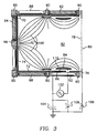
- a large electrode 70 has a side wall 72 which continues into end wall 74 but is open at its other end 76. Spanning open end 76 is a screen grid 78 followed by a parallel accelerator grid 80. Spaced within the interior region 82 from end 76 is a ring-shaped smaller electrode 84 having an outer surface 86 placed closely adjacent to inner wall 72 of electrode 70.
- Alongside and outside of end wall 74 of electrode 70 are once again a circumferentially-spaced plurality of permanent magnets 94 but this time held by pole pieces 90 and a central permeable pole piece 96 in the manner that magnets 94 resemble the spokes of a wheel. All of pole pieces 90 are essentially the same, although as indicated by the drawings different ones are slightly modified so as to appropriately receive the different magnets located at different places around the assembly.
- the magnet arrangement develops a magnetic field having the shape shown by the representative arrows 100.
- that field configuration may be assumed to be axially symmetric although axial symmetry is not as such a requirement for proper operation.
- An RF power source or supply 102 is coupled directly between ring electrode 84 and larger surrounding electrode 70. Electrode 70 is returned to ground through a capacitor 104. Ring electrode 84 may be referred to as the driven or excitation electrode and it am well as RF grounded electrode 70 are at the same average dc potential so that the potential variation on electrode 84 is approximately symmetrical about the potential on electrode 70.
- Electrode 70 has a rough similarity in function to grounded electrode 12 of the RF diode in Figure 1.
- RF electrode 84 has a function which is roughly similar to that of excitation electrode 14 in the diode of Figure 1. Note, however, that the plasma source of Figure 3 does not include the equivalent of capacitor 18 in the Figure 1 device to there provide dc isolation. This is because it has been found that the inclusion of such a capacitor in the Figure 3 system results in decreased ion generation efficiency.
- the ion energy available for acceleration in the plasma source of Figure 3 is determined by the positive potential of dc power source 106. Ions produced within plasma region 82 are accelerated through apertures in screen grid 78, which is electrically isolated from the other electrodes, and accelerator grid 80 which is maintained at a negative potential relative to ground by dc power supply 108. The negative potential on accelerator grid 80 prevents the back flow of electrons from the ion beam (electron backstreaming). As is usual and conventional with sources of this kind, the accelerated ion beam must be neutralized with the addition of electrons as typically supplied from a separate neutralizer filament which is not shown but is described more fully in the aforementioned Kaufman patent No. 3,156,090.
- the surrounding vacuum chamber which is understood to be necessary for operation. That vacuum chamber is also assumed to be held to ground potential.
- a plasma consisting of electrons and ions is generated in region 82 as a result of energy delivered from RF source 102.
- the strength of magnetic field 100 and the energy and mean path length for the electrons developed are such that the conductivity of the plasma parallel to the magnetic field is much greater than the conductivity transverse to that magnetic field. This is in accordance with the strong-field approximation of plasma physics.
- the ions that reach the ion optics of screen grid 78 and accelerator grid 80 are accelerated to form an energetic ion beam which, as indicated in the introduction and throughout the ion source prior art, can be used in a variety of propulsive and industrial applications.
- the magnetic field strength is significant near RF excitation electrode 84.
- the interior surface 110 that faces plasma region 82 is shaped and formed to be approximately parallel to the direction of the magnetic field. In this case where the field configuration is as shown, surface 110 is given a convex shape from the inner to the outer sides of ring 84.
- the portion of magnetic field 100 near electrode 84 is configured so that the field strength is given a broad minimum near electrode 84, a field strength which increases in both directions (to the left and right in Figure 3) away from electrode 84.
- Such a configuration of the magnetic field has been found to be very effective in generating ions at a low pressure of neutral molecules and while operating with low electrode voltages.
- the plasma sheaths adjacent to electrodes 70 and 84 constitute a capacitive load upon RF source 102 while at the same time there is a resistivity present as a result of electron collisions within the plasma that fills interior region 82 and which causes the dissipation of RF energy as the atoms are ionized.
- the sheaths and plasma are omitted from Figure 3 to show the magnetic field, but they have a rough similarity to sheaths 22 and 24 and plasma 20 in Figure 1.
- excitation electrode surface 110 and the direction of magnetic field 100 serves to minimize the sheath voltage between electrode 84 and the plasma developed in region 82.
- surface and the field direction not parallel, much higher RF currents would be required to generate the same plasma density, with those higher currents serving to generate higher sheath voltages.
- most of the RF power would be dissipated near the portion of electrode 84 that penetrates deepest into the magnetic field inasmuch as electrical contact with other portions of the adjacent plasma would then be established by a much higher than optimum conductivity parallel to the magnetic field.
- Another important factor in the localization of the RF heating is the containment by the magnetic field of the secondary electrons from ion collisions with the RF excitation electrode. In a conventional RF diode, those electrons add to the electron energy throughout the plasma so as to avoid a localized effect. Although a magnetic field parallel to RF excitation electrode 84 greatly improves the RF heating efficiency, it also contains the secondary electrons and thus serves to localize the energy input when a large sheath voltage is also present.
- RF electrode 84 Adding most of the RF energy into RF electrode 84 results in the development of a sheath that is larger than the sheath voltage at electrode 70, in a manner which is roughly similar to the area-ratio effect of the conventional RF diode as described in the aforementioned Kaufman and Rossnagel article. Because electrode 84 is located at the side of region 82, any sputter contamination from electrode 84 is unlikely to escape through screen grid 78 and accelerator grid 80 to the target of the ion beam. The likelihood of escape for sputtered material from electrode 84 can be further reduced by reducing the diameter of the portions of grids 78 and 80 with apertures, in effect hiding RF electrode 84 behind unapertured portions screen grid 78.
- the discharge chamber was sixteen centimeters in diameter.
- the magnetic field strength immediately above electrode 84 was about 0.01 Tesla (100 Gauss), and the neutral pressure in the plasma region (using either argon or oxygen) was less than one milliTorr (less than 0.1 Pascal). Under those conditions and using 500 watts of RF energy at 13.56 MHz, a 200 mA beam of ions was extracted.
- the operating voltages on RF electrode 84 were within ⁇ 50 volts of the voltage on electrode 70 with the result of minimal sputtering of electrode 84.
- Screen grid 78 assumed a potential of ten-twenty volts negative of electrode 70 so as again to result in little sputtering.
- Figure 3 specifically illustrates and has been described with respect to the use of grids so as to achieve electrostatic acceleration of the ions. Nevertheless, the ionization plasma process effected by the apparatus of Figure 3 may instead be used in apparatus where the acceleration is achieved by electromagnetic action as is the acceleration mechanism, for example, in U.S. patent No. 4,862,032 issued August 29, 1989, which discloses and claims an end-Hall ion source.
- the present approach may be incorporated into other devices using grids as known in the art to include one, two or three such grids.
- the ion optics may be omitted to allow ion energy ions and electrons to escape and directly provide low-energy ion bombardment or the electron neutralization of an ion beam.
- the loss of neutral gas from region 82 could be reduced by replacing screen grid 78 with a flat plate having a single central aperture, with that plate either electrically isolated or connected to electrode 70.
- a second feature of the present invention useful in itself to enhance energy transfer to a low-pressure plasma, is the combination of magnetic structure and electrode orientation so as in a plasma device to cause the magnetic field to be substantially parallel to the surface of the RF electrode. Adding, then, the additional contribution of magnetic field orientation so as to produce a field strength variation that tends to contain the energetic electrons affords in itself a different important increase in plasma generation efficiency.
Landscapes
- Engineering & Computer Science (AREA)
- Physics & Mathematics (AREA)
- Plasma & Fusion (AREA)
- Chemical & Material Sciences (AREA)
- Analytical Chemistry (AREA)
- Electromagnetism (AREA)
- Combustion & Propulsion (AREA)
- Spectroscopy & Molecular Physics (AREA)
- Electron Sources, Ion Sources (AREA)
- Plasma Technology (AREA)
- Chemical Vapour Deposition (AREA)
- Lock And Its Accessories (AREA)
- Injection Moulding Of Plastics Or The Like (AREA)
- Input Circuits Of Receivers And Coupling Of Receivers And Audio Equipment (AREA)
Applications Claiming Priority (2)
| Application Number | Priority Date | Filing Date | Title |
|---|---|---|---|
| US57679690A | 1990-08-31 | 1990-08-31 | |
| US576796 | 1995-12-21 |
Publications (3)
| Publication Number | Publication Date |
|---|---|
| EP0474584A2 true EP0474584A2 (fr) | 1992-03-11 |
| EP0474584A3 EP0474584A3 (en) | 1992-07-15 |
| EP0474584B1 EP0474584B1 (fr) | 1997-03-05 |
Family
ID=24306028
Family Applications (1)
| Application Number | Title | Priority Date | Filing Date |
|---|---|---|---|
| EP91630060A Expired - Lifetime EP0474584B1 (fr) | 1990-08-31 | 1991-08-29 | Source de plasma radiofréquence à couplage capacitif |
Country Status (8)
| Country | Link |
|---|---|
| EP (1) | EP0474584B1 (fr) |
| JP (1) | JPH0810633B2 (fr) |
| AT (1) | ATE149781T1 (fr) |
| CA (1) | CA2049876C (fr) |
| DE (2) | DE474584T1 (fr) |
| DK (1) | DK0474584T3 (fr) |
| ES (1) | ES2030376T3 (fr) |
| GR (2) | GR920300058T1 (fr) |
Cited By (3)
| Publication number | Priority date | Publication date | Assignee | Title |
|---|---|---|---|---|
| WO1998022969A1 (fr) * | 1996-11-18 | 1998-05-28 | Plasma Tech Co., Ltd. | Appareil a decharge gazeuse |
| RU2263995C2 (ru) * | 2003-05-30 | 2005-11-10 | Кошкин Валерий Викторович | Устройство высокочастотное для вакуумно-плазменной обработки поверхности |
| CN107340139A (zh) * | 2017-06-21 | 2017-11-10 | 北京卫星环境工程研究所 | 电推进航天器系统级点火试验溅射靶装置 |
Families Citing this family (4)
| Publication number | Priority date | Publication date | Assignee | Title |
|---|---|---|---|---|
| US5325021A (en) * | 1992-04-09 | 1994-06-28 | Clemson University | Radio-frequency powered glow discharge device and method with high voltage interface |
| US9536725B2 (en) | 2013-02-05 | 2017-01-03 | Clemson University | Means of introducing an analyte into liquid sampling atmospheric pressure glow discharge |
| DE102015215051A1 (de) * | 2015-08-06 | 2017-02-09 | Terraplasma Gmbh | Vorrichtung und Verfahren zum Erzeugen eines Plasmas, sowie Verwendung einer solchen Vorrichtung |
| WO2019152970A1 (fr) | 2018-02-05 | 2019-08-08 | Clemson University Research Foundation | Fibres canalisées dans la séparation de nanoparticules biologiquement actives |
-
1991
- 1991-08-26 CA CA002049876A patent/CA2049876C/fr not_active Expired - Lifetime
- 1991-08-29 ES ES91630060T patent/ES2030376T3/es not_active Expired - Lifetime
- 1991-08-29 DK DK91630060.1T patent/DK0474584T3/da active
- 1991-08-29 DE DE199191630060T patent/DE474584T1/de active Pending
- 1991-08-29 EP EP91630060A patent/EP0474584B1/fr not_active Expired - Lifetime
- 1991-08-29 AT AT91630060T patent/ATE149781T1/de not_active IP Right Cessation
- 1991-08-29 DE DE69124882T patent/DE69124882T2/de not_active Expired - Fee Related
- 1991-08-30 JP JP3299986A patent/JPH0810633B2/ja not_active Expired - Fee Related
-
1992
- 1992-08-31 GR GR92300058T patent/GR920300058T1/el unknown
-
1997
- 1997-06-04 GR GR970401296T patent/GR3023652T3/el unknown
Non-Patent Citations (3)
| Title |
|---|
| IBM TECHNICAL DISCLOSURE BULLETIN. vol. 24, no. 11B, April 1982, NEW YORK US pages 5833 - 5835; C GUARNIERI , H KAUFMAN: 'RF ION SOURCE' * |
| JOURNAL OF VACUUM SCIENCE AND TECHNOLOGY: PART A. vol. 6, no. 4, August 1988, NEW YORK US pages 2572 - 2573; H KAUFMAN: 'ANALYSIS OF AREA-RATIO EFFECT FOR RADIO-FREQUENCY DIODE' * |
| JOURNAL OF VACUUM SCIENCE AND TECHNOLOGY: PART B. vol. 6, no. 1, February 1988, NEW YORK US R LOSSY, J ENGEMANN: 'CHARACTERISATION OF A REACTIVE BROAD BEAM RADIO-FREQUENCY ION SOURCE' * |
Cited By (4)
| Publication number | Priority date | Publication date | Assignee | Title |
|---|---|---|---|---|
| WO1998022969A1 (fr) * | 1996-11-18 | 1998-05-28 | Plasma Tech Co., Ltd. | Appareil a decharge gazeuse |
| US6040547A (en) * | 1996-11-18 | 2000-03-21 | Plasma Tech Co., Ltd. | Gas discharge device |
| RU2263995C2 (ru) * | 2003-05-30 | 2005-11-10 | Кошкин Валерий Викторович | Устройство высокочастотное для вакуумно-плазменной обработки поверхности |
| CN107340139A (zh) * | 2017-06-21 | 2017-11-10 | 北京卫星环境工程研究所 | 电推进航天器系统级点火试验溅射靶装置 |
Also Published As
| Publication number | Publication date |
|---|---|
| DE69124882D1 (de) | 1997-04-10 |
| GR920300058T1 (en) | 1992-08-31 |
| JPH0689798A (ja) | 1994-03-29 |
| ES2030376T1 (es) | 1992-11-01 |
| DE474584T1 (de) | 1992-08-13 |
| DE69124882T2 (de) | 1997-09-04 |
| JPH0810633B2 (ja) | 1996-01-31 |
| DK0474584T3 (da) | 1997-09-08 |
| GR3023652T3 (en) | 1997-09-30 |
| ATE149781T1 (de) | 1997-03-15 |
| EP0474584B1 (fr) | 1997-03-05 |
| CA2049876A1 (fr) | 1992-03-01 |
| ES2030376T3 (es) | 1997-07-01 |
| CA2049876C (fr) | 1998-02-10 |
| EP0474584A3 (en) | 1992-07-15 |
Similar Documents
| Publication | Publication Date | Title |
|---|---|---|
| US5274306A (en) | Capacitively coupled radiofrequency plasma source | |
| US4778561A (en) | Electron cyclotron resonance plasma source | |
| US6803585B2 (en) | Electron-cyclotron resonance type ion beam source for ion implanter | |
| KR940010844B1 (ko) | 이온 원(源) | |
| US6254745B1 (en) | Ionized physical vapor deposition method and apparatus with magnetic bucket and concentric plasma and material source | |
| US5198718A (en) | Filamentless ion source for thin film processing and surface modification | |
| US7863582B2 (en) | Ion-beam source | |
| US7875867B2 (en) | Non-ambipolar radio-frequency plasma electron source and systems and methods for generating electron beams | |
| US4486665A (en) | Negative ion source | |
| US3969646A (en) | Electron-bombardment ion source including segmented anode of electrically conductive, magnetic material | |
| EP0115119A2 (fr) | Electrode de magnétron à champ conformé | |
| JP3123735B2 (ja) | イオンビーム処理装置 | |
| US4767931A (en) | Ion beam apparatus | |
| EP0474584B1 (fr) | Source de plasma radiofréquence à couplage capacitif | |
| US5432342A (en) | Method of and apparatus for generating low-energy neutral particle beam | |
| JP4029495B2 (ja) | イオン源 | |
| KR920003157B1 (ko) | PIG(Penning Ionization Gause)형의 이온원 | |
| JPH0589792A (ja) | サイクロトロン共鳴機能を備えたイオン源 | |
| CA2249157C (fr) | Implantation d'ions monoenergetiques de distribution uniforme | |
| US5256930A (en) | Cooled plasma source | |
| JPH0955170A (ja) | イオン源 | |
| JP3379227B2 (ja) | イオン源装置 | |
| JPH09259781A (ja) | イオン源装置 | |
| EP0095879B1 (fr) | Equipement et méthode pour le traitement des surfaces avec un faisceau d'ions à basse énergie et haute intensité | |
| JP2870473B2 (ja) | イオン源装置 |
Legal Events
| Date | Code | Title | Description |
|---|---|---|---|
| PUAI | Public reference made under article 153(3) epc to a published international application that has entered the european phase |
Free format text: ORIGINAL CODE: 0009012 |
|
| AK | Designated contracting states |
Kind code of ref document: A2 Designated state(s): AT BE CH DE DK ES FR GB GR IT LI LU NL SE |
|
| ITCL | It: translation for ep claims filed |
Representative=s name: RICCARDI SERGIO & CO. |
|
| PUAL | Search report despatched |
Free format text: ORIGINAL CODE: 0009013 |
|
| TCAT | At: translation of patent claims filed | ||
| EL | Fr: translation of claims filed | ||
| AK | Designated contracting states |
Kind code of ref document: A3 Designated state(s): AT BE CH DE DK ES FR GB GR IT LI LU NL SE |
|
| DET | De: translation of patent claims | ||
| TCNL | Nl: translation of patent claims filed | ||
| REG | Reference to a national code |
Ref country code: ES Ref legal event code: BA2A Ref document number: 2030376 Country of ref document: ES Kind code of ref document: T1 |
|
| 17P | Request for examination filed |
Effective date: 19920909 |
|
| GRAG | Despatch of communication of intention to grant |
Free format text: ORIGINAL CODE: EPIDOS AGRA |
|
| 17Q | First examination report despatched |
Effective date: 19960417 |
|
| GRAH | Despatch of communication of intention to grant a patent |
Free format text: ORIGINAL CODE: EPIDOS IGRA |
|
| GRAH | Despatch of communication of intention to grant a patent |
Free format text: ORIGINAL CODE: EPIDOS IGRA |
|
| GRAA | (expected) grant |
Free format text: ORIGINAL CODE: 0009210 |
|
| AK | Designated contracting states |
Kind code of ref document: B1 Designated state(s): AT BE CH DE DK ES FR GB GR IT LI LU NL SE |
|
| REF | Corresponds to: |
Ref document number: 149781 Country of ref document: AT Date of ref document: 19970315 Kind code of ref document: T |
|
| REG | Reference to a national code |
Ref country code: CH Ref legal event code: EP |
|
| REF | Corresponds to: |
Ref document number: 69124882 Country of ref document: DE Date of ref document: 19970410 |
|
| ITF | It: translation for a ep patent filed | ||
| ET | Fr: translation filed | ||
| REG | Reference to a national code |
Ref country code: ES Ref legal event code: FG2A Ref document number: 2030376 Country of ref document: ES Kind code of ref document: T3 |
|
| REG | Reference to a national code |
Ref country code: GR Ref legal event code: FG4A Free format text: 3023652 |
|
| REG | Reference to a national code |
Ref country code: DK Ref legal event code: T3 |
|
| PLBE | No opposition filed within time limit |
Free format text: ORIGINAL CODE: 0009261 |
|
| 26N | No opposition filed | ||
| PGFP | Annual fee paid to national office [announced via postgrant information from national office to epo] |
Ref country code: BE Payment date: 19980727 Year of fee payment: 8 Ref country code: DK Payment date: 19980727 Year of fee payment: 8 Ref country code: SE Payment date: 19980727 Year of fee payment: 8 |
|
| PGFP | Annual fee paid to national office [announced via postgrant information from national office to epo] |
Ref country code: LU Payment date: 19980731 Year of fee payment: 8 |
|
| PGFP | Annual fee paid to national office [announced via postgrant information from national office to epo] |
Ref country code: CH Payment date: 19980804 Year of fee payment: 8 |
|
| PGFP | Annual fee paid to national office [announced via postgrant information from national office to epo] |
Ref country code: ES Payment date: 19980817 Year of fee payment: 8 |
|
| PGFP | Annual fee paid to national office [announced via postgrant information from national office to epo] |
Ref country code: GR Payment date: 19980819 Year of fee payment: 8 |
|
| PG25 | Lapsed in a contracting state [announced via postgrant information from national office to epo] |
Ref country code: LU Free format text: LAPSE BECAUSE OF NON-PAYMENT OF DUE FEES Effective date: 19990829 Ref country code: DK Free format text: LAPSE BECAUSE OF NON-PAYMENT OF DUE FEES Effective date: 19990829 |
|
| PG25 | Lapsed in a contracting state [announced via postgrant information from national office to epo] |
Ref country code: ES Free format text: LAPSE BECAUSE OF NON-PAYMENT OF DUE FEES Effective date: 19990830 Ref country code: SE Free format text: THE PATENT HAS BEEN ANNULLED BY A DECISION OF A NATIONAL AUTHORITY Effective date: 19990830 |
|
| PG25 | Lapsed in a contracting state [announced via postgrant information from national office to epo] |
Ref country code: LI Free format text: LAPSE BECAUSE OF NON-PAYMENT OF DUE FEES Effective date: 19990831 Ref country code: BE Free format text: LAPSE BECAUSE OF NON-PAYMENT OF DUE FEES Effective date: 19990831 Ref country code: GR Free format text: THE PATENT HAS BEEN ANNULLED BY A DECISION OF A NATIONAL AUTHORITY Effective date: 19990831 Ref country code: CH Free format text: LAPSE BECAUSE OF NON-PAYMENT OF DUE FEES Effective date: 19990831 |
|
| BERE | Be: lapsed |
Owner name: KAUFMAN & ROBINSON INC. Effective date: 19990831 |
|
| REG | Reference to a national code |
Ref country code: CH Ref legal event code: PL |
|
| EUG | Se: european patent has lapsed |
Ref document number: 91630060.1 |
|
| REG | Reference to a national code |
Ref country code: DK Ref legal event code: EBP |
|
| REG | Reference to a national code |
Ref country code: GB Ref legal event code: IF02 |
|
| REG | Reference to a national code |
Ref country code: ES Ref legal event code: FD2A Effective date: 20000911 |
|
| PGFP | Annual fee paid to national office [announced via postgrant information from national office to epo] |
Ref country code: NL Payment date: 20050812 Year of fee payment: 15 Ref country code: FR Payment date: 20050812 Year of fee payment: 15 Ref country code: DE Payment date: 20050812 Year of fee payment: 15 |
|
| PGFP | Annual fee paid to national office [announced via postgrant information from national office to epo] |
Ref country code: AT Payment date: 20050816 Year of fee payment: 15 |
|
| PGFP | Annual fee paid to national office [announced via postgrant information from national office to epo] |
Ref country code: GB Payment date: 20050822 Year of fee payment: 15 |
|
| PG25 | Lapsed in a contracting state [announced via postgrant information from national office to epo] |
Ref country code: IT Free format text: LAPSE BECAUSE OF NON-PAYMENT OF DUE FEES;WARNING: LAPSES OF ITALIAN PATENTS WITH EFFECTIVE DATE BEFORE 2007 MAY HAVE OCCURRED AT ANY TIME BEFORE 2007. THE CORRECT EFFECTIVE DATE MAY BE DIFFERENT FROM THE ONE RECORDED. Effective date: 20050829 |
|
| PG25 | Lapsed in a contracting state [announced via postgrant information from national office to epo] |
Ref country code: AT Free format text: LAPSE BECAUSE OF NON-PAYMENT OF DUE FEES Effective date: 20060829 |
|
| PG25 | Lapsed in a contracting state [announced via postgrant information from national office to epo] |
Ref country code: DE Free format text: LAPSE BECAUSE OF NON-PAYMENT OF DUE FEES Effective date: 20070301 Ref country code: NL Free format text: LAPSE BECAUSE OF NON-PAYMENT OF DUE FEES Effective date: 20070301 |
|
| GBPC | Gb: european patent ceased through non-payment of renewal fee |
Effective date: 20060829 |
|
| NLV4 | Nl: lapsed or anulled due to non-payment of the annual fee |
Effective date: 20070301 |
|
| REG | Reference to a national code |
Ref country code: FR Ref legal event code: ST Effective date: 20070430 |
|
| PG25 | Lapsed in a contracting state [announced via postgrant information from national office to epo] |
Ref country code: GB Free format text: LAPSE BECAUSE OF NON-PAYMENT OF DUE FEES Effective date: 20060829 |
|
| PG25 | Lapsed in a contracting state [announced via postgrant information from national office to epo] |
Ref country code: FR Free format text: LAPSE BECAUSE OF NON-PAYMENT OF DUE FEES Effective date: 20060831 |