EP0473574B1 - Verfahren zum formen einer zielelektrode für das elektrostatische aufladen einer faserstruktur - Google Patents
Verfahren zum formen einer zielelektrode für das elektrostatische aufladen einer faserstruktur Download PDFInfo
- Publication number
- EP0473574B1 EP0473574B1 EP89906224A EP89906224A EP0473574B1 EP 0473574 B1 EP0473574 B1 EP 0473574B1 EP 89906224 A EP89906224 A EP 89906224A EP 89906224 A EP89906224 A EP 89906224A EP 0473574 B1 EP0473574 B1 EP 0473574B1
- Authority
- EP
- European Patent Office
- Prior art keywords
- surface layer
- dielectric surface
- mold cavity
- target electrode
- process according
- Prior art date
- Legal status (The legal status is an assumption and is not a legal conclusion. Google has not performed a legal analysis and makes no representation as to the accuracy of the status listed.)
- Expired - Lifetime
Links
Images

Classifications
-
- D—TEXTILES; PAPER
- D01—NATURAL OR MAN-MADE THREADS OR FIBRES; SPINNING
- D01D—MECHANICAL METHODS OR APPARATUS IN THE MANUFACTURE OF ARTIFICIAL FILAMENTS, THREADS, FIBRES, BRISTLES OR RIBBONS
- D01D5/00—Formation of filaments, threads, or the like
- D01D5/11—Flash-spinning
-
- B—PERFORMING OPERATIONS; TRANSPORTING
- B29—WORKING OF PLASTICS; WORKING OF SUBSTANCES IN A PLASTIC STATE IN GENERAL
- B29C—SHAPING OR JOINING OF PLASTICS; SHAPING OF MATERIAL IN A PLASTIC STATE, NOT OTHERWISE PROVIDED FOR; AFTER-TREATMENT OF THE SHAPED PRODUCTS, e.g. REPAIRING
- B29C35/00—Heating, cooling or curing, e.g. crosslinking or vulcanising; Apparatus therefor
- B29C35/16—Cooling
-
- B—PERFORMING OPERATIONS; TRANSPORTING
- B29—WORKING OF PLASTICS; WORKING OF SUBSTANCES IN A PLASTIC STATE IN GENERAL
- B29C—SHAPING OR JOINING OF PLASTICS; SHAPING OF MATERIAL IN A PLASTIC STATE, NOT OTHERWISE PROVIDED FOR; AFTER-TREATMENT OF THE SHAPED PRODUCTS, e.g. REPAIRING
- B29C43/00—Compression moulding, i.e. applying external pressure to flow the moulding material; Apparatus therefor
- B29C43/02—Compression moulding, i.e. applying external pressure to flow the moulding material; Apparatus therefor of articles of definite length, i.e. discrete articles
- B29C43/18—Compression moulding, i.e. applying external pressure to flow the moulding material; Apparatus therefor of articles of definite length, i.e. discrete articles incorporating preformed parts or layers, e.g. compression moulding around inserts or for coating articles
-
- B—PERFORMING OPERATIONS; TRANSPORTING
- B29—WORKING OF PLASTICS; WORKING OF SUBSTANCES IN A PLASTIC STATE IN GENERAL
- B29C—SHAPING OR JOINING OF PLASTICS; SHAPING OF MATERIAL IN A PLASTIC STATE, NOT OTHERWISE PROVIDED FOR; AFTER-TREATMENT OF THE SHAPED PRODUCTS, e.g. REPAIRING
- B29C43/00—Compression moulding, i.e. applying external pressure to flow the moulding material; Apparatus therefor
- B29C43/32—Component parts, details or accessories; Auxiliary operations
- B29C43/44—Compression means for making articles of indefinite length
- B29C43/48—Endless belts
-
- B—PERFORMING OPERATIONS; TRANSPORTING
- B29—WORKING OF PLASTICS; WORKING OF SUBSTANCES IN A PLASTIC STATE IN GENERAL
- B29C—SHAPING OR JOINING OF PLASTICS; SHAPING OF MATERIAL IN A PLASTIC STATE, NOT OTHERWISE PROVIDED FOR; AFTER-TREATMENT OF THE SHAPED PRODUCTS, e.g. REPAIRING
- B29C43/00—Compression moulding, i.e. applying external pressure to flow the moulding material; Apparatus therefor
- B29C43/32—Component parts, details or accessories; Auxiliary operations
- B29C43/52—Heating or cooling
-
- B—PERFORMING OPERATIONS; TRANSPORTING
- B29—WORKING OF PLASTICS; WORKING OF SUBSTANCES IN A PLASTIC STATE IN GENERAL
- B29C—SHAPING OR JOINING OF PLASTICS; SHAPING OF MATERIAL IN A PLASTIC STATE, NOT OTHERWISE PROVIDED FOR; AFTER-TREATMENT OF THE SHAPED PRODUCTS, e.g. REPAIRING
- B29C43/00—Compression moulding, i.e. applying external pressure to flow the moulding material; Apparatus therefor
- B29C43/32—Component parts, details or accessories; Auxiliary operations
- B29C43/44—Compression means for making articles of indefinite length
- B29C43/48—Endless belts
- B29C2043/486—Endless belts cooperating with rollers or drums
-
- B—PERFORMING OPERATIONS; TRANSPORTING
- B29—WORKING OF PLASTICS; WORKING OF SUBSTANCES IN A PLASTIC STATE IN GENERAL
- B29K—INDEXING SCHEME ASSOCIATED WITH SUBCLASSES B29B, B29C OR B29D, RELATING TO MOULDING MATERIALS OR TO MATERIALS FOR MOULDS, REINFORCEMENTS, FILLERS OR PREFORMED PARTS, e.g. INSERTS
- B29K2019/00—Use of rubber not provided for in a single one of main groups B29K2007/00 - B29K2011/00, as moulding material
-
- B—PERFORMING OPERATIONS; TRANSPORTING
- B29—WORKING OF PLASTICS; WORKING OF SUBSTANCES IN A PLASTIC STATE IN GENERAL
- B29K—INDEXING SCHEME ASSOCIATED WITH SUBCLASSES B29B, B29C OR B29D, RELATING TO MOULDING MATERIALS OR TO MATERIALS FOR MOULDS, REINFORCEMENTS, FILLERS OR PREFORMED PARTS, e.g. INSERTS
- B29K2021/00—Use of unspecified rubbers as moulding material
-
- B—PERFORMING OPERATIONS; TRANSPORTING
- B29—WORKING OF PLASTICS; WORKING OF SUBSTANCES IN A PLASTIC STATE IN GENERAL
- B29K—INDEXING SCHEME ASSOCIATED WITH SUBCLASSES B29B, B29C OR B29D, RELATING TO MOULDING MATERIALS OR TO MATERIALS FOR MOULDS, REINFORCEMENTS, FILLERS OR PREFORMED PARTS, e.g. INSERTS
- B29K2303/00—Use of resin-bonded materials as reinforcement
- B29K2303/04—Inorganic materials
- B29K2303/06—Metal powders, metal carbides or the like
-
- B—PERFORMING OPERATIONS; TRANSPORTING
- B29—WORKING OF PLASTICS; WORKING OF SUBSTANCES IN A PLASTIC STATE IN GENERAL
- B29K—INDEXING SCHEME ASSOCIATED WITH SUBCLASSES B29B, B29C OR B29D, RELATING TO MOULDING MATERIALS OR TO MATERIALS FOR MOULDS, REINFORCEMENTS, FILLERS OR PREFORMED PARTS, e.g. INSERTS
- B29K2705/00—Use of metals, their alloys or their compounds, for preformed parts, e.g. for inserts
-
- B—PERFORMING OPERATIONS; TRANSPORTING
- B29—WORKING OF PLASTICS; WORKING OF SUBSTANCES IN A PLASTIC STATE IN GENERAL
- B29K—INDEXING SCHEME ASSOCIATED WITH SUBCLASSES B29B, B29C OR B29D, RELATING TO MOULDING MATERIALS OR TO MATERIALS FOR MOULDS, REINFORCEMENTS, FILLERS OR PREFORMED PARTS, e.g. INSERTS
- B29K2995/00—Properties of moulding materials, reinforcements, fillers, preformed parts or moulds
- B29K2995/0003—Properties of moulding materials, reinforcements, fillers, preformed parts or moulds having particular electrical or magnetic properties, e.g. piezoelectric
- B29K2995/0006—Dielectric
Definitions
- This invention relates to the manufacture of dielectric surfaces of target electrodes used in the application of electrostatic charge to fibrous structures, and relates more particularly to the process for molding dielectric surface layers of target electrodes used in the application of electrostatic charge to multifibrous webs during manufacture thereof by flash-spinning, subsequent charging and spreading, and depositing onto a moving surface.
- Processes and apparatus for flash-spinning multifibrous web structures of interconnecting fibrous filaments, including target electrodes used in electrostatic charging of thusly spun fibrous structures for spreading and depositing thereof, are known in the art.
- U.S. Patent No. 3,578,739 issued to George discloses an apparatus for applying electrostatic charge to flash-spun fibrous structures, wherein the fibrous structures pass through a charging zone between a corona discharge electrode and a target electrode, the target electrode having a conductive base and a high-resistance surface covering.
- the high-resistance dielectric surface covering is provided to reduce a problem-causing effect associated with flash-spinning and electrostatic charging of fibrous structures, namely the generation of small separated particles which become attracted to the target electrode and build up an electrically insulating film thereupon.
- U.S. Patent No. 3,860,369 to Brethauer et al also discloses an apparatus for making non-woven fibrous sheets, and including electrostatic charging of the web in a corona discharge zone that includes a metal disc target electrode which is preferably covered with a dielectric insulating surface as disclosed in U.S. Patent No. 3,578,739.
- U.S. Patent No. 3,689,608 to Hollberg et al discloses a process for forming a nonwoven web that includes electrostatic charging of the web in a corona discharge zone between an ion gun and an all-metal target plate.
- fouling particle deposits collecting upon metal target electrodes rapidly reduce the effectiveness of electrostatic charging of the web for the reason and in the manner hereinbefore indicated in conjunction with U.S. Patent No. 3,578,739.
- the present invention is intended to substantially reduce the aforesaid problems associated with target electrodes that have resulted in relatively short useful operating life for heretofore known target electrodes and surface coverings therefor, and accordingly, the invention has as a primary object the provision of a process for molding of a dielectric target surface layer to significantly reduce the rate of loss in charging efficiency caused by in-process degradation of the surface layer and by flash-spun fouling deposits accumulating upon the target electrode in the course of electrostatic charging of the fibrous structure that is being fed to and along the target surface, so that useful target surface layer operating lifetimes are achieved that are significantly longer than heretofore possible.
- regions on the target electrode exposed to corona discharge are molded over with a dielectric surface layer, that comprises a rubber copolymer formulation of primarily acrilonitrile/butadiene and phenolic resin hardener.
- the dielectric surface layer molding process serves to achieve a substantially defect-free surface layer that is flat, smooth, and continuous, and that has a hardness in the range of 75 to 85 Shore A Durometer, while voids and air or gas inclusions are substantially avoided within the layer and between the layer and the metal target base.
- the substantially homogeneous dielectric surface layer covers and adheres intimately to surfaces and edges of the metal target base.
- the process further includes removal of mold flashing to substantially eliminate irregular surfaces and to leave surfaces smooth.
- the molding process comprises cleaning of the metal target base and installation thereof in a preheated mold cavity, that has been treated with release agent, loading of the mold cavity with milled material in accordance with the material formulation for the dielectric surface layer, closure of heated mold and loading thereof through compression cycles, and curing of the molded layer (while disposed in mold).
- the metal target base together with the dielectric surface layer molded thereover is removed from the mold and the combination part is post-treated for a cooling time whilst being compression loaded between parallel plates.
- a flash-spinning apparatus 10 is schematically depicted therein that is used in production of multifibrous web structures.
- the shown apparatus comprises charging means for electrostatically charging such structures.
- the charging means includes an ion gun 12 and a target electrode 14; the latter being generally shaped in form of an annular disc.
- Target electrode 14 is provided with a dielectric surface layer 16, and is concentrically disposed about a baffle 18.
- Baffle 18 is revolved about axis 20, as indicated by arrow 22.
- a spinneret 24 is supplied with a pressurized polymer solution that issues from orifice 28 and forms a fibrous structure 26.
- An aerodynamic shield comprises a first member 30 and a second member 32.
- Target electrode 14 together with second member 32 are adapted to be rotated independently of baffle 18, but concentrically therewith, by means not shown here.
- a collecting surface 34 is comprised in an endless belt 36 that is carried by rolls of a powered conveyor means 38.
- Ion gun 12 comprised in first shield member 30, is supplied with a potential of 50 to 100 kilovolts.
- Target electrode 14 is connected to electrical ground via a here not shown contact ring and brush arrangement.
- a corona discharge is produced between ion gun 12 and target electrode 14, and continuously charges fibrous structure 26, thereby causing spreading thereof.
- Collecting surface 34 is electrically conductive and is grounded or given an opposite charge relative to the charge imposed on fibrous structure 26. Consequently, fibrous structure 26 is attracted to and deposited upon collecting surface 34 in flattened sheet-like form and is conveyed by powered conveyor means 38 to an accumulating means 42.
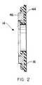
- target electrode 14 is shown therein in an enlarged sectional view.
- Target electrode 14 comprises a metal target base 44 covered over most of its surface by dielectric surface layer 16.
- Dielectric surface layer 16 extends over target base 44 at least over those regions that are directly exposed to corona discharge.
- Target electrode 14 has an approximate shape of an annular disc having a ring-like contact mount member 46 of target base 44 protruding from one face thereof. At least a portion of contact mount member 46 remains uncovered by dielectric surface layer 16 to facilitate electrical connection to ground, as hereinbefore indicated in conjunction with FIG.1.
- a portion of the flat face of target electrode 14 faces toward ion gun 12.
- the thickness of dielectric surface layer 16, at least where it is disposed over the region of the flat face of target electrode 14, is preferably about 1.5 mm thick, although other thicknesses can be used, particularly to accommodate various sizes of flash-spinning apparatus 10.
- Dielectric surface layer 16 is preferably compression molded over target base 44, although other molding methods can be applied satisfactorily.
- a preferred target electrode 14 (including its dielectric surface layer) has approximate dimensions of 19.05 centimeters for its outer diameter, 10.16 centimeters for its inside diameter, and approximately 79.4 millimeters for the thickness of its metal target base 44, while its dielectric surface layer is approximately 15.9 millimeters thick.
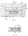
- a portion of a hot press molding apparatus is shown to include a mold base 50 and a mold compression member 52.
- a mold cavity 54 is removably disposed in mold base 50.
- Metal target base 44 is seated in a recess 58 within mold base 50.
- a closure plate 60 removably covers mold cavity 54, enclosing therein a cavity 62 that is disposed between outer surfaces of metal target base 44 and inside surfaces of mold cavity 54 and closure plate 60.
- the region of cavity 62 is shaped to correspond to the shape of dielectric surface layer 16 (that is to be molded), and is shown here to contain a dielectric surface layer as molded over metal target base 44.
- Mold compression member 52 fits slidably into the upper opening of mold base 50 to facilitate compression loading of the contents of cavity 62 within mold cavity 54 via closure plate 60.
- the applied compression loading force is schematically indicated here by a force arrow 64.
- Heat transfer by heating of mold base 50, including the components contained therein, is schematically indicated by heat transfer arrow 66.
- a cooling fixture arrangement comprises a top plate 68 and a bottom plate 70 in parallel relationship, having disposed therebetween the metal target base 44 with dielectric surface layer 16 molded thereover.
- This arrangement serves for post-treatment of the molded dielectric surface layer by cooling (from the molding temperature) whilst being subjected to compression loading in its flat facial region to enhance its surface properties and its intimate adhesion to metal target base 44.
- This post-treatment also promotes closure of any tiny voids in dielectric surface layer 16.
- Compression arrow 72 indicates schematically the compression loading force applied during the post-treatment.
- the dielectric surface layer material formulation is cured in the closed mold cavity 54 in the hot press apparatus under substantially constant compression loading and at a substantially constant curing temperature.
- the curing conditions preferably comprise a compression load of about 22.727 kgs. (for a target electrode in the preferred size hereinbefore indicated) and a temperature of about 150 to 155 degrees C for a curing time of about 20 to 25 minutes.
- the present invention provides a process for molding of dielectric surface layer 16 having intimate contact with the metal target base 44 of target electrode 14, the dielectric surface layer 16 extending at least over those regions upon target electrode 14 that are directly exposed to corona discharge.
- Dielectric surface layer 16 comprises a rubber copolymer formulation of acrylonitrile/butadiene and phenolic resin hardener, exhibiting a hardness in the range of 75 to 85 Shore A Durometer and a volume resistivity between 2x10⁹ and 2x10¹⁰ ohm-cm when measured at 60 degrees C and 1000 volts.
- the dielectric surface layer 16 of the present invention has exhibited a rate of increase in voltage thereacross of no more than 1 to 2 KV per 24 hours when tested at constant charging supply current. This represents a 3 to 8 fold improvement over the rate of voltage increase exhibited by good quality prior art target coatings which were tested under identical conditions.
- on-line tests under actual process conditions showed a lifetime of less than 100 hours for over 75 percent of the number of prior art target coatings tested, the lifetime being established by the time to process failure due to target coating failure.
- the remainder of less than 25 percent of the prior art target coatings exhibited an average rate of voltage increase of about 3.3 KV per 24 hours.
- targets coated with the dielectric surface layer 16 according to the present invention when on-line tested under indentical actual process conditions, showed a substantially lesser average voltage increase rate of about 1.2 KV per 24 hours. It will be appreciated that these results indicate a very significant increase in useful lifetimes for the dielectric surface layer 16 of the present invention, this lifetime increase being at least about three-fold and as much as about eight-fold or more in actual practice.
- the significance of the voltage (and therewith the resistance) across a dielectric surface layer of a target electrode is based in the hereinbefore described breakdown effect. As the voltage drop increases across the layer (due to resistivity increase under operating conditions), the material breakdown potential is approached and eventually reached. Thereafter, charging effectiveness is rapidly degraded and lost and the process fails. Therefore, the material properties of the dielectric surface layer are of critical importance to the process. Particularly, resistivity and voltage drop across the layer and the stability thereof in the operating environment are of crucial significance.
- the operating environment includes corona bombardment in a solvent vapor atmosphere at temperatures of 60 degrees C and higher. Similarly, the reproducibility of these properties, of the physical dimensions of the surface layer, and of its surface quality are key factors in the provision of a suitable material and in the molding thereof.
- the molded dielectric surface layer of the present invention has an increased hardness in the range of 75 to 85 and preferably at least 81 to 82 Shore A Durometer.
- the dielectric surface layer material of the present invention comprises rubber copolymer formulations of acrylonitrile/butadiene and phenolic resin that provide the described properties and characteristics.
- the rubber copolymer formulations comprise primarily acrylonitrile/butadiene and phenolic resin, and further include zinc oxide for vulcanization enhancement, carbon black for resistivity control, stearic acid to enhance crosslinking associated with vulcanization, and curing accelerators.
- preferred rubber copolymer formulations comprise 100 parts of acrylonitrile/butadiene (in a ratio of 35 to 65, respectively), 25 to 30 parts of phenolic resin, 5 to 5.5 parts of zinc oxide, 10 parts of carbon black, 1.5 parts of stearic acid, and 3 parts of curing accelerators.
- the phenolic resin component is reduced toward the lower end of the above given range, preferably to 25 parts, and the stearic acid component is increased to preferably 5.5 parts.
- the properties of the dielectric surface layer are of great importance to its satisfactory in-process performance in the application of electrostatic charge to flash-spun fibrous structures. Not only the particular material formulation of the dielectric surface layer, but equally so the applied molding process establish these properties. Proper molding process conditions are critical to the achievement of desirable properties, and significant changes in these conditions can easily result in a short life or unacceptable performance of the dielectric surface layer.
- the molding process per se, for instance, particularly also critically influences the achievability of homogeneity and hardness of the dielectric surface layer, of continuous and smooth surfaces substantially free of defects, such as scratches, nicks, and cracks, of substantial absence of voids and air or gas inclusions within the layer and at the interface thereof with the metal target base over which it is molded, and of intimate adhesion between the molded dielectric surface layer and the metal target base.
Landscapes
- Engineering & Computer Science (AREA)
- Mechanical Engineering (AREA)
- Textile Engineering (AREA)
- Physics & Mathematics (AREA)
- Health & Medical Sciences (AREA)
- Oral & Maxillofacial Surgery (AREA)
- Thermal Sciences (AREA)
- Casting Or Compression Moulding Of Plastics Or The Like (AREA)
- Spinning Methods And Devices For Manufacturing Artificial Fibers (AREA)
Claims (10)
- Verfahren zum Formen einer dielektrischen Oberflächenschicht einer Anodenelektrode (14), welche zum elektrostatischen Aufladen von Flash-gesponnenen Fasergebilden eingesetzt wird, welches folgende Schritte aufweist:a. Reinigen einer Metallanodenbasis (44);b. Vorwärmen und Einführen eines Formhohlraums (54) in eine Heißpreßvorrichtung, wobei der Formhohlraum derart ausgebildet ist, daß die Metallanodenbasis (44) aufgenommen wird, und wobei ein Trennmittel auf die Oberflächen in dem Formhohlraum aufgebracht wird;c. Einbauen der Metallanodenbasis in den Formhohlraum (54);d. Einbringen einer Materialformulierung für die dielektrische Oberflächenschicht in den Formhohlraum (54) und Schließen des Formhohlraums mittels einer Verschlußplatte (60), um einen geschlossenen Formhohlraum (62) zu bilden, wobei der geschlossene Formhohlraum darin einen Bereich bereitstellt, welcher im wesentlichen der dielektrischen Oberflächenschicht (16) der Anodenelektrode zugeordnet ist, wobei die Materialformulierung für die dielektrische Oberflächenschicht hauptsächlich eine Kautschukcopolymerformulierung aus Acrylonitril/Butadien und Phenolharzhärter aufweist;e. Aufbringen von einem oder mehreren Verdichtungszyklen auf den geschlossenen Formhohlraum in und mittels der Heißpreßvorrichtung, wobei dieser einen oder mehrere Verdichtungszyklen mit einer Verdichtungsbelastung auf den geschlossenen Formhohlraum auf etwa 4,545 Kilogramm und anschließendem Entlasten der Verdichtungsbelastung und anschließendem Aufbringen einer Verdichtungsbelastung auf den geschlossenen Formhohlraum (62) auf etwa 22.727 Kilogramm aufweist, wobei dieser eine oder mehrere Verdichtungszyklen ausgeführt wird oder werden, während dem die geschlossene Form (62) im wesentlichen auf einer Temperatur von etwa 160°C gehalten ist, und Härten der Materialformulierung für die dielektrische Oberflächenschicht in dem geschlossenen Formhohlraum unter einer Härtungstemperatur und Härtungsverdichtungs-Belastungsbedingungen, wobei die Materialformulierungfür die dielektrische Oberflächenschicht (16) geformt und in inniger haftender Verbindung hierdurch an den Oberflächen der Metallanodenbasis (44) gebracht wird; undf. Entfernen der Kombination aus Metallanodenbasis (44) mit der Materialformulierung für die dielektrische Oberflächenschicht (16) aus dem geschlossenen Formhohlraum (62) und Abkühlen der Kombination unter Verdichtungsbelastung.
- Verfahren nach Anspruch 1, bei dem das Vorerwärmen gemäß dem Schritt (b) bei einer Temperatur von etwa 160°C erfolgt.
- Verfahren nach Anspruch 1, bei dem die Materialformulierung für die dielektrische Oberflächenschicht (16) ferner Zinkoxid zur Vulkanisierungsunterstützung, Ruß für die Einstellung des spezifischen Widerstands, Stearinsäure zur Unterstützung der mit der Vulkanisierung einhergehenden Vernetzung und Härtungsbeschleuniger umfaßt.
- Verfahren nach Anspruch 1, bei dem die Materialformulierung für die dielektrische Oberflächenschicht (16) im wesentlichen 100 Teile Acrilonitril/Butadien in einem Verhältnis von 35 bis 65 jeweils, 25 bis 30 Teile Phenolharz, 5 bis 5,5 Teile Zinkoxid, 10 Teile Ruß, 1,5 Teile Stearinsäure und drei Teile Härtungsbeschleuniger aufweist.
- Verfahren nach Anspruch 1, bei dem die Härtungstemperatur und die Härtungsverdichtungs-Belastungsbedingungen im Schritt (e) 150 bis 155 °C und etwa 22,727 Kilogramm jeweils während einem Zeitraum von 20 bis 25 Minuten umfassen.
- Verfahren nach Anspruch 1, bei dem das Kühlen im Schritt (f) unter Verdichtungsbelastung von etwa 13,6 Kilogramm während einer so ausreichenden Zeit erfolgt, daß die Anodenelektrode (14) Raumtemperatur erreicht, wobei die Verdichtungsbelastung zwischen der ebenen Fläche der dielektrischen Oberflächenschicht (16) der Anodenelektrode und der Metallanodenbasis (44) aufgebracht wird.
- Verfahren nach Anspruch 1, bei dem wenigstens ein Teil der dielektrischen Oberflächenschicht (16) der Anodenelektrode eine Dicke von etwa 1,5 mm hat.
- Verfahren nach Anspruch 1, bei dem die dielektrische Oberflächenschicht (16) der Anodenelektrode eine Härte in einem Bereich von 75 bis 85 Shore A Durometer hat.
- Verfahren nach Anspruch 1, bei dem die dielektrische Oberflächenschicht (16) der Anodenelektrode einen spezifischen Durchgangswiderstand in einem Bereich von etwa 2x10⁹ bis 2x10¹⁰ Ohm-cm gemessen bei 60°C und 1000 Volt hat.
- Verfahren nach Anspruch 1, bei dem die dielektrische Oberfläche (16) der Anodenelektrode eine Spannungszunahmerate von nicht größer als 1 bis 2 KV pro 24 Stunden hat, wenn eine Test bei konstantem Ladestrom unter normalen Flashspinn-Betriebsbedingungen erfolgt.
Applications Claiming Priority (1)
| Application Number | Priority Date | Filing Date | Title |
|---|---|---|---|
| PCT/US1989/002002 WO1990014202A1 (en) | 1989-05-15 | 1989-05-15 | Process for molding target electrode used in the application of electrostatic charge to a fibrous structure |
Publications (3)
| Publication Number | Publication Date |
|---|---|
| EP0473574A1 EP0473574A1 (de) | 1992-03-11 |
| EP0473574A4 EP0473574A4 (en) | 1992-06-03 |
| EP0473574B1 true EP0473574B1 (de) | 1994-12-28 |
Family
ID=22215001
Family Applications (1)
| Application Number | Title | Priority Date | Filing Date |
|---|---|---|---|
| EP89906224A Expired - Lifetime EP0473574B1 (de) | 1989-05-15 | 1989-05-15 | Verfahren zum formen einer zielelektrode für das elektrostatische aufladen einer faserstruktur |
Country Status (5)
| Country | Link |
|---|---|
| EP (1) | EP0473574B1 (de) |
| JP (1) | JPH04505130A (de) |
| HK (1) | HK82395A (de) |
| SG (1) | SG30613G (de) |
| WO (1) | WO1990014202A1 (de) |
Families Citing this family (2)
| Publication number | Priority date | Publication date | Assignee | Title |
|---|---|---|---|---|
| DE4316154C1 (de) * | 1993-05-14 | 1994-04-21 | Daimler Benz Ag | Verfahren zur sichtseitigen Beschichtung eines Innenausbauteiles |
| KR102019456B1 (ko) * | 2012-01-23 | 2019-09-06 | 닛뽕 카바이도 고교 가부시키가이샤 | 금형 청소용 수지 조성물 |
Family Cites Families (14)
| Publication number | Priority date | Publication date | Assignee | Title |
|---|---|---|---|---|
| CA598235A (en) * | 1960-05-17 | J. B. Coulter David | Bonding process | |
| FR1205511A (fr) * | 1957-04-26 | 1960-02-03 | Ciba Geigy | Procédé pour réaliser des enveloppes constituées par des couches minces, exemptes de fissures, isolantes au point de vue électrique, autour de pièces métalliques,au moyen de masses de résines artificielles |
| US3387326A (en) * | 1964-06-04 | 1968-06-11 | Du Pont | Apparatus for charging and spreading a web |
| US4183841A (en) * | 1965-07-16 | 1980-01-15 | The United States Of America As Represented By The Secretary Of The Navy | Filled composition containing phenol-aldehyde resin and butadiene-acrylonitrile polymer |
| FR1482969A (fr) * | 1966-04-18 | 1967-06-02 | Dalle de revêtement de sol et procédé de fabrication de celle-ci | |
| US3578739A (en) * | 1969-05-13 | 1971-05-18 | Du Pont | Apparatus for applying electrostatic charge to fibrous structure |
| GB1283719A (en) * | 1969-10-14 | 1972-08-02 | Rolls Royce | Coating process |
| US3860369A (en) * | 1972-11-02 | 1975-01-14 | Du Pont | Apparatus for making non-woven fibrous sheet |
| US4036668A (en) * | 1972-11-17 | 1977-07-19 | Caterpillar Tractor Co. | Bonding fluoroelastomers to metal |
| JPS5327290A (en) * | 1976-08-27 | 1978-03-14 | Yamada Toshihito | Device for automatically picking and shaking blood |
| US4359438A (en) * | 1981-09-21 | 1982-11-16 | Ashland Oil, Inc. | Process for molding corrosion resistant fuel cell collecting plates |
| JPS58101037A (ja) * | 1981-11-24 | 1983-06-16 | Japan Synthetic Rubber Co Ltd | フツ素ゴムとブタジエン−アクリロニトリル共重合ゴムとの加硫接着方法 |
| US4704176A (en) * | 1984-12-19 | 1987-11-03 | The Goodyear Tire & Rubber Company | Method of bonding polyurethane to cured rubber |
| JPH0677932B2 (ja) * | 1986-12-09 | 1994-10-05 | 古河電気工業株式会社 | エポキシ樹脂注型品の製造方法 |
-
1989
- 1989-05-15 SG SG1995906087A patent/SG30613G/en unknown
- 1989-05-15 WO PCT/US1989/002002 patent/WO1990014202A1/en not_active Ceased
- 1989-05-15 EP EP89906224A patent/EP0473574B1/de not_active Expired - Lifetime
- 1989-05-15 JP JP1506012A patent/JPH04505130A/ja active Pending
-
1995
- 1995-05-25 HK HK82395A patent/HK82395A/en not_active IP Right Cessation
Also Published As
| Publication number | Publication date |
|---|---|
| WO1990014202A1 (en) | 1990-11-29 |
| EP0473574A1 (de) | 1992-03-11 |
| SG30613G (en) | 1995-09-01 |
| EP0473574A4 (en) | 1992-06-03 |
| JPH04505130A (ja) | 1992-09-10 |
| HK82395A (en) | 1995-06-01 |
Similar Documents
| Publication | Publication Date | Title |
|---|---|---|
| EP0008542B1 (de) | Verfahren zum Herstellung einer xerographischen Schmelzfixierwalze mit antiadhäsiver Oberfläche | |
| US5585426A (en) | Process for imparting an electrostatic charge to powders to render them useful for coating application | |
| AU707667B2 (en) | Apparatus for coating substrates with inductively charged resinous powder particles | |
| US4230068A (en) | Apparatus used in continuous process for electrostatic coating with pulverized material | |
| US2701765A (en) | Xerographic fusing apparatus | |
| JP2003518906A (ja) | 吹付焼結法を用いる回転電気機械の電気的導体又は導体束の高品質絶縁体の製造方法 | |
| EP0534671B1 (de) | Abgabewalze aus Phenolharz und Graphit | |
| US5494619A (en) | Improved electrostatic pinning method | |
| EP0473574B1 (de) | Verfahren zum formen einer zielelektrode für das elektrostatische aufladen einer faserstruktur | |
| US5756164A (en) | Triboelectric coating powder and process | |
| US5385761A (en) | Discharge element, method of producing the same and apparatus comprising the same | |
| WO1990014228A1 (en) | Improved dielectric surface for electrostatic charge target | |
| US4218493A (en) | Electrostatic repair coating | |
| US2555519A (en) | Method of painting electrostatically nonconducting articles | |
| US3940518A (en) | Bake technique for manufacturing tetrafluoroethylene coated rolls | |
| EP0938385B1 (de) | Verfahren und vorrichtung zum transferieren von zusätzlichem material auf die oberfläche eines beweglichen materialnetzes | |
| CN115106263A (zh) | 一种可以使涂层满足高压绝缘要求的喷涂方法 | |
| JPS562126A (en) | Method and apparatus for manufacturing polymer film | |
| CN113717584A (zh) | 一种新型稳定塑粉及其制备方法 | |
| CA1103102A (en) | Continuous process for electrostatic coating with pulverized material and apparatus used in said process | |
| SU1609713A1 (ru) | Способ получени листового армированного полимерного композита | |
| JP2009183810A (ja) | 静電作用を利用した塗装方法 | |
| CA2201878C (en) | Process for imparting an electrostatic charge to powders to render them useful for coating applications | |
| JPS642429B2 (de) | ||
| JPS6119415B2 (de) |
Legal Events
| Date | Code | Title | Description |
|---|---|---|---|
| PUAI | Public reference made under article 153(3) epc to a published international application that has entered the european phase |
Free format text: ORIGINAL CODE: 0009012 |
|
| 17P | Request for examination filed |
Effective date: 19911129 |
|
| AK | Designated contracting states |
Kind code of ref document: A1 Designated state(s): GB LU |
|
| A4 | Supplementary search report drawn up and despatched |
Effective date: 19920413 |
|
| AK | Designated contracting states |
Kind code of ref document: A4 Designated state(s): GB LU |
|
| 17Q | First examination report despatched |
Effective date: 19930820 |
|
| GRAA | (expected) grant |
Free format text: ORIGINAL CODE: 0009210 |
|
| AK | Designated contracting states |
Kind code of ref document: B1 Designated state(s): GB LU |
|
| PG25 | Lapsed in a contracting state [announced via postgrant information from national office to epo] |
Ref country code: LU Free format text: LAPSE BECAUSE OF NON-PAYMENT OF DUE FEES Effective date: 19950531 |
|
| PLBE | No opposition filed within time limit |
Free format text: ORIGINAL CODE: 0009261 |
|
| STAA | Information on the status of an ep patent application or granted ep patent |
Free format text: STATUS: NO OPPOSITION FILED WITHIN TIME LIMIT |
|
| 26N | No opposition filed | ||
| PGFP | Annual fee paid to national office [announced via postgrant information from national office to epo] |
Ref country code: GB Payment date: 19960404 Year of fee payment: 8 |
|
| PG25 | Lapsed in a contracting state [announced via postgrant information from national office to epo] |
Ref country code: GB Effective date: 19970515 |
|
| GBPC | Gb: european patent ceased through non-payment of renewal fee |
Effective date: 19970515 |
|
| ITF | It: translation for a ep patent filed |