EP0473440B1 - Filtre optique de longueur d'onde et son procédé de commande - Google Patents
Filtre optique de longueur d'onde et son procédé de commande Download PDFInfo
- Publication number
- EP0473440B1 EP0473440B1 EP91307934A EP91307934A EP0473440B1 EP 0473440 B1 EP0473440 B1 EP 0473440B1 EP 91307934 A EP91307934 A EP 91307934A EP 91307934 A EP91307934 A EP 91307934A EP 0473440 B1 EP0473440 B1 EP 0473440B1
- Authority
- EP
- European Patent Office
- Prior art keywords
- mode
- waveguide
- filter
- electrode means
- mode converter
- Prior art date
- Legal status (The legal status is an assumption and is not a legal conclusion. Google has not performed a legal analysis and makes no representation as to the accuracy of the status listed.)
- Expired - Lifetime
Links
Images


Classifications
-
- G—PHYSICS
- G02—OPTICS
- G02F—OPTICAL DEVICES OR ARRANGEMENTS FOR THE CONTROL OF LIGHT BY MODIFICATION OF THE OPTICAL PROPERTIES OF THE MEDIA OF THE ELEMENTS INVOLVED THEREIN; NON-LINEAR OPTICS; FREQUENCY-CHANGING OF LIGHT; OPTICAL LOGIC ELEMENTS; OPTICAL ANALOGUE/DIGITAL CONVERTERS
- G02F1/00—Devices or arrangements for the control of the intensity, colour, phase, polarisation or direction of light arriving from an independent light source, e.g. switching, gating or modulating; Non-linear optics
- G02F1/01—Devices or arrangements for the control of the intensity, colour, phase, polarisation or direction of light arriving from an independent light source, e.g. switching, gating or modulating; Non-linear optics for the control of the intensity, phase, polarisation or colour
- G02F1/03—Devices or arrangements for the control of the intensity, colour, phase, polarisation or direction of light arriving from an independent light source, e.g. switching, gating or modulating; Non-linear optics for the control of the intensity, phase, polarisation or colour based on ceramics or electro-optical crystals, e.g. exhibiting Pockels effect or Kerr effect
- G02F1/035—Devices or arrangements for the control of the intensity, colour, phase, polarisation or direction of light arriving from an independent light source, e.g. switching, gating or modulating; Non-linear optics for the control of the intensity, phase, polarisation or colour based on ceramics or electro-optical crystals, e.g. exhibiting Pockels effect or Kerr effect in an optical waveguide structure
- G02F1/0353—Devices or arrangements for the control of the intensity, colour, phase, polarisation or direction of light arriving from an independent light source, e.g. switching, gating or modulating; Non-linear optics for the control of the intensity, phase, polarisation or colour based on ceramics or electro-optical crystals, e.g. exhibiting Pockels effect or Kerr effect in an optical waveguide structure involving an electro-optic TE-TM mode conversion
-
- G—PHYSICS
- G02—OPTICS
- G02F—OPTICAL DEVICES OR ARRANGEMENTS FOR THE CONTROL OF LIGHT BY MODIFICATION OF THE OPTICAL PROPERTIES OF THE MEDIA OF THE ELEMENTS INVOLVED THEREIN; NON-LINEAR OPTICS; FREQUENCY-CHANGING OF LIGHT; OPTICAL LOGIC ELEMENTS; OPTICAL ANALOGUE/DIGITAL CONVERTERS
- G02F1/00—Devices or arrangements for the control of the intensity, colour, phase, polarisation or direction of light arriving from an independent light source, e.g. switching, gating or modulating; Non-linear optics
- G02F1/01—Devices or arrangements for the control of the intensity, colour, phase, polarisation or direction of light arriving from an independent light source, e.g. switching, gating or modulating; Non-linear optics for the control of the intensity, phase, polarisation or colour
- G02F1/0136—Devices or arrangements for the control of the intensity, colour, phase, polarisation or direction of light arriving from an independent light source, e.g. switching, gating or modulating; Non-linear optics for the control of the intensity, phase, polarisation or colour for the control of polarisation, e.g. state of polarisation [SOP] control, polarisation scrambling, TE-TM mode conversion or separation
- G02F1/0142—TE-TM mode conversion
-
- G—PHYSICS
- G02—OPTICS
- G02F—OPTICAL DEVICES OR ARRANGEMENTS FOR THE CONTROL OF LIGHT BY MODIFICATION OF THE OPTICAL PROPERTIES OF THE MEDIA OF THE ELEMENTS INVOLVED THEREIN; NON-LINEAR OPTICS; FREQUENCY-CHANGING OF LIGHT; OPTICAL LOGIC ELEMENTS; OPTICAL ANALOGUE/DIGITAL CONVERTERS
- G02F2201/00—Constructional arrangements not provided for in groups G02F1/00 - G02F7/00
- G02F2201/12—Constructional arrangements not provided for in groups G02F1/00 - G02F7/00 electrode
- G02F2201/124—Constructional arrangements not provided for in groups G02F1/00 - G02F7/00 electrode interdigital
-
- G—PHYSICS
- G02—OPTICS
- G02F—OPTICAL DEVICES OR ARRANGEMENTS FOR THE CONTROL OF LIGHT BY MODIFICATION OF THE OPTICAL PROPERTIES OF THE MEDIA OF THE ELEMENTS INVOLVED THEREIN; NON-LINEAR OPTICS; FREQUENCY-CHANGING OF LIGHT; OPTICAL LOGIC ELEMENTS; OPTICAL ANALOGUE/DIGITAL CONVERTERS
- G02F2203/00—Function characteristic
- G02F2203/05—Function characteristic wavelength dependent
- G02F2203/055—Function characteristic wavelength dependent wavelength filtering
Definitions
- the present invention relates to an optical wavelength selection filter which comprises a waveguide formed on a substrate; an input polarizer at an input to the waveguide, having a first polarization planer an output polarizer at an output of the waveguide, having a second different polarization plane; and a mode converter disposed along the waveguide between the polarizers for converting radiation from a first mode polarized in said first plane to a second mode polarized in said second plane, the mode converter comprising a multi-fingered reference electrode means interdigitated with a plurality of finger-like control electrode means.
- the present invention also relates to a method of tuning an optical wavelength selection filter.
- a known optical wavelength selection filter is disclosed in "Heisemann, F. et al., Electronics Letters, 23 (1987), 21st May, No. 11".
- the tuning range of the disclosed filter is only 8nm which is insufficient for practical application.
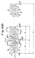
- FIG. 1 Another filter structure is illustrated in Fig. 1. This structure has been proposed in order to provide an improvement in tuning range for optical filters.
- the optical wavelength filter illustrated in the Fig. 1 comprises a waveguide path 12 formed in a substrate 10, polarizers 14 and 16 disposed respectively at an input port 12a and an output port 12b of the waveguide path 12, and three mode converters 18 disposed between the polarizers 14,16.
- a waveguide type polarizer 14 transmits TE mode light
- a waveguide type polarizer 16 transmits TM mode light
- the mode converters 18 convert TE mode light having a predetermined wavelength into TM mode light.
- light having a predetermined wavelength can be selected from polychromatic light.
- the mode converters 18 are configured such that the centre wavelengths ⁇ o of their bandwidths differ by ⁇ T (max) from that of the adjacent mode converter(s) 18, where ⁇ T (max) is the maximum tuning deviation of each mode converter 18.
- Each mode converter 18 is constituted by a pair of interdigitated multi-fingered electrodes.
- the multi-fingered electrodes 18a are located at predetermined locations along the waveguide path 12.
- the periods of the multi-finger electrodes 18a of each mode converter 18 differ from converter to converter. Consequently, the centre wavelengths ⁇ o of the mode converters differ from each other.
- optical mode conversion can be performed on a predetermined wavelength.
- the length L of the mode converter must be increased.
- the conventional filter necessitates a plurality of mode converters 18 being coupled in series to select light having a predetermined wavelength.
- the total length of the optical wavelength filter is required to be, at least, nL.
- an optical wavelength selection filter includes controllable voltage generator means for applying a voltage pattern to the control electrode means, wherein the voltage pattern is or approximates a spatial sine wave and the voltage generator means is controllable to vary the period of said sine wave.
- the present invention also provides a method of tuning an optical wavelength selection filter which comprises a waveguide formed on a substrate; an input polarizer at an input to the waveguide, having a first polarization plane; an output polarizer at an output of the waveguide, having a second different polarization plane; and a mode converter disposed along the waveguide between the polarizers for converting radiation from a first mode polarized in said first plane to a second mode polarized in said second plane, the converter comprising a multi-fingered reference electrode means interdigitated with a plurality of finger-type control electrode means.
- a method according to the present invention comprises the steps of:
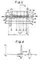
- an optical wavelength filter employs a front stage polarizer 20 for transmitting input TM light, a plurality of mode converter sections 22 for converting the input TM light, having a wavelength for which they are active, into TM light, and a rear stage polarizer 24 for transmitting the TE light from the mode converter sections 22 for output.
- the polarizers 20,24 and the mode converter sections 22 are formed along a waveguide path 26.
- the mode converter sections 22 each comprise finger-type control electrodes 28 and finger-type earthing electrodes 30.
- the control and earthing electrodes 28,30 are interdigitated with each other and extend transversely across the waveguide path 26.
- the waveguide path 26 is in the form of straight line and is formed by diffusing Ti in a X-cut LiNbO 3 substrate 32.
- the front stage polarizer 20 is disposed at the input port 26a of the waveguide path 26 and the rear stage polarizer 24 is disposed at the output port 26b.
- the polarizers 20,24 are waveguide types.
- the finger-type electrodes 28,30 within each mode converter section 22 are coupled by common conductors 34,38 to form comb-shaped control and earthing electrode structures.
- All of the electrodes 28 and 30 disposed between the front and the rear stage polarizers 20 and 24 are disposed with an equal interval G.
- the lengths 1 of the mode converter sections 22 are the same.
- the length 1 is defined as a distance between a position G/2 in the direction toward the front stage polarizer 20 from the first electrode of a mode converter section 22 and a position G/2 in the direction toward the rear stage polarizer 24 from the last electrode of the mode converter section 22.
- the letter L shown in Figs. 2 (A) and 2 (B), represents the overall length of the mode-conversion portion of an optical wavelength filter.
- the total length L corresponds to the length of a single mode converter 18 employed in the optical wavelength filter shown in Fig. 1.
- the "period" of the distribution of the mode converter sections 22 is ⁇ 1 which equals 2.l.
- the letter W represents the width of an electrode and in this embodiment all the finger-type electrodes 28,30 have the same width.
- T, t, G, l, L, ⁇ 1 and W is defined as a distance along the waveguide path 26.
- control voltages applied to the control electrodes 28 are such that the electric field distribution in the waveguide path 26 approximates the product of two sine waves.
- the same voltage Vm is applied to every electrode 28 belonging to the same mode converter section 22, where m is the mode converter index, the mode converter section nearest the input port having the index 1, the next the index 2 and so on.
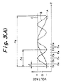
- Fig. 3 (A) shows a distribution of the voltage Vm in which the vertical axis represents voltage V and the horizontal axis represents a position z in a direction along the waveguide path 26.
- the letter Cm representing the position of the m-th mode converter section 22 along the waveguide path 26, can mean either the starting, the ending or the centre position.
- An appropriate position C1 is chosen on the z-axis and positions C2, C3, Vietnamese are sequentially set from the position C1 with an interval l.
- the voltage Vm applied to the control electrode 28 which belongs to the m-th mode converter section 22, located at the position Cm, is plotted as a black circle in the drawing.
- the voltage Vm is set for driving the optical wavelength filter such that the distribution of the voltage Vm approximates a sine wave form as illustrated as black circles on curves A or B in Figure 3 (A).
- control voltage distribution is an accurate sine wave.
- the curves A and B are, for example, represented as V - sin z and the period of the curves A and B equals a period ⁇ 2 described later (refer to Fig. 3 (B)).
- the vertical axis represents strength of electric field generated in the waveguide path 26 in the direction of the thickness of a substrate and the horizontal axis represents the distance z along the waveguide path 26.
- the distribution of electric field e(z) is a step-wise approximation to the product of two sine waves.
- the distribution of electric field e(z) varies step-wise as described above, the distribution of electric field e(z) can be analogously considered to be a smoothly varying distribution of electric field E(z) when the length 1 of the mode converter section 22 is extremely small.
- Fig. 4 shows the smoothly varying distribution of electric field E(z) and envelopes I and II thereof, in which the vertical axis represents strength of electric field in the waveguide path 26 in the direction of the thickness of the substrate and the horizontal axis represents the distance z along the waveguide path 26.
- the second term (e i. ⁇ .z ⁇ e -i. ⁇ .z ) of the equation A represents the "modulation" of the distribution E(z); the "carrier” wave form of which approximates a sine-wave.
- ⁇ n and ⁇ 0 are predetermined structural design parameters and the optical wavelength ⁇ transmitting through the optical wavelength filter can be varied by varying the period ⁇ 2 of the voltage Vm.
- the equation (G) clearly teaches that the optical wavelength filter can transmit light having the two wavelengths ⁇ 0 + ⁇ T and ⁇ 0 - ⁇ T .
- an optical wavelength filter can be achieved which is transmit light having two wavelengths ⁇ 0 + ⁇ T and ⁇ 0 - ⁇ T .
- K(z) is approximately described as follows:
- the term f 0 (z) corresponds to the main peak of the light with a converted wavelength and equals the equation (D).
- f j (z) in case of j ⁇ 0 corresponds to the peak of the noise light.
- the band width ⁇ W of the embodiment equals that shown in Fig. 1, assuming the lengths L of both elements are equal.
- the operational voltage of the optical wavelength filter according to the embodiment is approximately 1.5 times larger than that of the optical wavelength filter shown in Fig. 1.
- N Nmax / 2.
- the total length of the optical wavelength filter shown in Fig. 1 needs to be n-times larger than that of the embodiment.
- a computer may be employed to control the voltages Vm applied to the mode converter sections 22.
- a second embodiment of the invention is constituted such that the length 1 of the mode converter sections 22 becomes shorter (or longer) sequentially along a direction of arrangement.
- the total numbers of the finger-type electrodes 28,30 employed in the mode converter sections 22 increase or decrease depending on the increase or decrease of the length L.
- a mode converter section 22 may contain one or more control and earthing electrodes 28,30.
- One mode converter section 22 constituted by a single finger-type electrode 28 for control and a single finger-type electrode 30 for earthing is shown in the drawing enclosed by the one-doted line indicated by the letter S.
- Fig. 6 is an explanatory view of noise light, wherein the vertical axis represents conversion efficiency ⁇ of TM/TE mode conversion and the horizontal axis represents an optical wavelength ⁇ .
- Fig. 6 shows the conversion efficiency ⁇ between the TM and TE modes wavelength ⁇ for a filter according to the first embodiment of the present invention.
- the mode-conversion of the light having a conversion wavelength (or an approximate conversion wavelength failing into the band width M having the band width ⁇ w from the central conversion wavelength) occurs and, in addition to that, the conversion efficiency ⁇ of the noise light (the light failing into the image wavelength band width N) is elevated to exceed -10dB at the peak value when the period ⁇ 2 approaches to the period ⁇ 1 .
- the length l of the mode converter 22 of the second embodiment is set to be gradually shorter or longer sequentially, the conversion efficiency of the noise light can be reduced, whereby the peak value of the conversion efficiency of the noise light can be reduced to below -10dB even though the period ⁇ 2 approaches to the period ⁇ 1 .
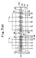
- Figs. 7 (A) ⁇ (C) are explanatory views of the embodiment according to the invention, wherein Fig. 7 (A) is a perspective view schematically illustrating the total construction of the third embodiment and Fig. 7 (B) is an enlarged plan view mainly illustrating the arrangement of the first mode converter, and Fig. 7 (C) is an enlarged plan view mainly illustrating the arrangement of a second mode converter.
- An optical wavelength filter employs, as shown in Fig. 7 (A), a front stage polarizer 54 for transmitting input TM mode light, a plurality of the first mode converter sections 56 for mode-converting input TM mode light, a middle stage polarizer 58 for transmitting the TE mode light from the first mode converter 56, a plurality of the second mode converter sections 60 for mode converting the TE mode light into TM mode light, and a rear stage polarizer 62 for transmitting the TM mode light from the second mode converter 60 as output light, all of which are disposed along the wave guide path 26.
- the first and the second mode converter sections 56,60 are respectively constituted by a combination of interdigitally disposed finger-type electrodes 28 for control and finger-type electrodes 30 for earthing.
- a front stage polarizer 54 located adjacent the input port 26a of the wave guide path 26, a rear stage polarizer 62 located adjacent the output port 26b, and a middle stage polarizer 58 between these polarizers 54 and 62.
- the polarizers 54, 58 and 62 are wave guide-type polarizers.
- the first element group I is formed such that a plurality of the first mode converter sections 56 are disposed between the front stage polarizer 54 and the middle stage polarizer 58.
- the second group II is formed such that a plurality of the second mode converter sections 60 are disposed between the middle stage polarizer 58 and the rear stage polarizer 62.
- the filter portion I which has a similar construction to the first embodiment, is constituted by the front stage polarizer 54, the middle stage polarizer 58 and a plurality of the first mode converter sections 56 between both these polarizers.
- the filter portion II which has a similar construction to the first embodiment, is constituted by the middle stage polarizer 58, the rear stage polarizer 62 and a plurality of the second-mode converter sections 60 between these polarizers.
- the filter portion I inputs the TM mode light from the input port 26a and converts the TM light having the conversion wavelength into TE mode light to be output.
- the filter portion II converts the TE mode light having the conversion wavelength selectively among the input TE mode light from the filter portion I into TM mode light to be output from the output port 26b.
- all the finger-type electrodes 28,30 disposed between the front and the middle stage polarizers 54 and 58 are disposed with the first interval (the disposed interval (electrode gap) is shown in Fig. 7 (B) at G1.) and all the finger-type electrodes 28,30 disposed between the middle and the rear stage polarizers 58,62 are disposed with the second interval (the disposed interval (electrode gap) is shown in Fig. 7 (C) at G2.).
- Figs. 7 (B) and 7 (C) represent the total lengths of the filter portions I and II
- Wl and W2 represent the electrode widths.
- This embodiment is constituted such that the electrode widths of the finger-type electrodes 28,30 in all the first mode converters 56 are commonly set to the electrode width W1 and the electrode width of the finger-type electrodes 28,30 in all the second mode converters 60 are commonly set to the electrode width W2.
- the electrode gap G1 is preferably set to be equal to the electrode width W1 and the electrode gap G2 equal to the electrode width W2 in the same way.
- each control electrode 28 is controlled such that the distribution of electric field e1(z) along the waveguide path 26 of the first mode converter sections 56 and the distribution of electric field e2(z) along the waveguide path 26 of the second mode converter sections 60 are both approximations of the product of two sine waves.
- the distributions of electric fields e1(z) and e2(z) are arranged such that mode conversion takes place in both filter portions I, II for light having the same free space wavelength.
- the distribution of electric field e1(z) is utilized for converting the TM mode light into the TE mode light in the filter portion I and the distribution of electric field e2(z) is utilized for converting the TE mode light into the TM mode light in the filter portion II.
- the first voltage Vn applied to the control electrodes 28 of the first mode converter sections 56 is controlled in order to mode-convert the TM mode light into TE mode light.
- the second voltage Un applied to the finger-type electrodes 28 of each second mode converter sections 60 is controlled in order to mode-convert the TE mode light into TM mode light.
- the distribution of electric field e1(z) and the first voltage Vn in the filter portion I and the distribution of electric field e2(z) and the second voltage Un in the filter portion II are controlled in the manner described with reference to the first embodiment.
- the conversion wavelength of the first mode converter sections 56 in the filter portion I is given as ⁇ 01 ⁇ ⁇ T1 , wherein ⁇ T1 varies in response to the variation of the period ⁇ 22 of the second voltage Un.
- Fig. 8 (A) the horizontal axis represents the optical wavelength ⁇ mode-converted in the filter portion I and the vertical axis represents the conversion efficiency ⁇
- Fig. 8 (B) the horizontal axis represents the optical wavelength ⁇ mode-converted in the filter portion II and the vertical axis represents the conversion efficiency ⁇ .
- the optical wavelength can be varied by controlling ⁇ T1 and ⁇ T2 , as is clear from Fig. 8.
- the channel number of the optical wavelength filter of the third embodiment is twice that of the first embodiment.
- This embodiment generates the first and the second distributions of electric field e1(z) and e2(z) concurrently and adjusts periods of both the first and the second voltages Vn and Un in such a manner that either of the two conversion wavelengths of filter portion I coincides with either of the two conversion wavelengths of the second mode converter 60 in the filter portion II, whereby a light with a desired wavelength can be selected from polychromatic light.
- the shape of the pass-band of a filter according to the present invention can be improved by setting the voltages, applied to the control electrodes 28, such that the mode conversion efficiency at the ends of the filter is less than that at the centre of the filter. This will be now be explained with reference to Figs. 8 and 10.
- Fig. 9 (A) illustrates a voltage Vm distribution applied to a filter according to the first embodiment of the present invention.
- the vertical axis is applied voltage (Vm) and the horizontal axis is displacement along the waveguide path (z).
- Fig. 9 (B) is a plot of conversion efficiency ( ⁇ ) against wavelength ( ⁇ ) where Vm is as shown in Fig. 9 (A). M indicates the filters pass-band.
- Figs. 10 (A) and (B) are respectively plots of applied control voltage against displacement along the waveguide path and efficiency against wavelength in the case where the applied voltage Vm is arranged such that the mode conversion efficiency at the ends of the filter is less than that at the centre of the filter.
- the embodiments according to the present invention enable filters to be constructed with bandwidths of approximately 1 nm and which are tunable over a range greater than 100 nm.
- the spacing between adjacent electrode pairs R is equal to G.
- R could be set to an integer multiple of G.
Landscapes
- Physics & Mathematics (AREA)
- Nonlinear Science (AREA)
- Chemical & Material Sciences (AREA)
- Engineering & Computer Science (AREA)
- Ceramic Engineering (AREA)
- Crystallography & Structural Chemistry (AREA)
- General Physics & Mathematics (AREA)
- Optics & Photonics (AREA)
- Optical Modulation, Optical Deflection, Nonlinear Optics, Optical Demodulation, Optical Logic Elements (AREA)
- Optical Integrated Circuits (AREA)
Claims (7)
- Filtre de sélection de longueurs d'onde optiques, comprenant un guide d'ondes (26) formé sur un substrat (32); un polariseur d'entrée (20) disposé à une entrée du guide d'ondes (26) et possédant un premier plan de polarisation; un polariseur de sortie (24) situé à une sortie du guide d'ondes (26) et possédant un second plan de polarisation différent; et un convertisseur de mode (22) disposé le long du guide d'ondes (26) entre les polariseurs (20,24) pour convertir le rayonnement depuis un premier mode polarisé dans ledit premier plan en un second mode polarisé dans ledit second plan, le convertisseur (22) comprenant des moyens formant électrodes de référence (36) à doigts multiples, interdigités avec une pluralité de moyens formant électrodes de commande (28) du type formés de doigts, caractérisé par des moyens formant générateur de tension commandable pour appliquer une forme de tension (A,B) aux moyens formant électrodes de commande (28), la forme de tension (A,B) étant ou se rapprochant d'une onde sinusoïdale spatiale et les moyens formant générateur de tension pouvant être commandés de manière à modifier la période de ladite onde sinusoïdale.
- Filtre selon la revendication 1, dans lequel l'espacement entre les éléments en forme de doigts (28,30) desdits moyens formant électrodes est constant le long du guide d'ondes (26) entre les polariseurs (20,24).
- Filtre selon la revendication 1 ou 2, dans lequel des groupes de moyens formant électrodes de commande voisins (28) sont couplés électriquement entre eux de manière à définir une pluralité de sections (22) de convertisseur de mode réparties le long du guide d'ondes (26).
- Filtre selon la revendication 3, dans lequel la périodicité des éléments en forme de doigts (28,30) des moyens formant électrodes de référence et de commande (36,34) est constante dans chaque section (22) du convertisseur de mode.
- Filtre selon la revendication 4, dnas lequel les longueurs des sections (22) du convertisseur de mode augmentent ou diminuent en direction du polariseur de sortie (24).
- Filtre de sélection de longueurs d'onde optiques comprenant deux filtres branchés en cascade selon l'une quelconque des revendications précédentes, le polariseur de sortie (58) d'un filtre agissant en tant que polariseur d'entrée pour le filtre suivant.
- Procédé pour accorder un filtre de sélection de longueurs d'onde optiques, qui comprend un guide d'ondes (26) formé sur un substrat (32); un polariseur d'entrée (20) disposé à une entrée du guide d'ondes (26) et possédant un premier plan de polarisation; un polariseur de sortie (24) situé à une sortie du guide d'ondes (26) et possédant un second plan de polarisation différent; et un convertisseur de mode (22) disposé le long du guide d'ondes (26) entre les polariseurs (20,24) pour convertir le rayonnement depuis un premier mode polarisé dans ledit premier plan en un second mode polarisé dans ledit second plan, le convertisseur (22) comprenant des moyens formant électrodes de référence (36) à doigts multiples, interdigités avec une pluralité de moyens formant électrodes de commande (34) du type formé de doigts, le procédé comprenant les étapes consistant à :(a) appliquer une première forme de tension (A,B) qui est ou se rapproche d'une onde sinusoïdale spatiale possédant une première période, aux moyens formant électrodes de commande (34), et(b) remplacer la première forme de tension (A,B) par une seconde forme de tension (A,B), qui est ou se rapproche d'une onde sinusoïdale spatiale possédant une seconde période, aux moyens formant électrodes de commande (34), pour accorder ainsi le filtre.
Applications Claiming Priority (2)
| Application Number | Priority Date | Filing Date | Title |
|---|---|---|---|
| JP228858/90 | 1990-08-30 | ||
| JP2228858A JP2902082B2 (ja) | 1990-08-30 | 1990-08-30 | 光波長フィルタ及びその駆動方法 |
Publications (3)
| Publication Number | Publication Date |
|---|---|
| EP0473440A2 EP0473440A2 (fr) | 1992-03-04 |
| EP0473440A3 EP0473440A3 (en) | 1992-09-23 |
| EP0473440B1 true EP0473440B1 (fr) | 1997-02-12 |
Family
ID=16882989
Family Applications (1)
| Application Number | Title | Priority Date | Filing Date |
|---|---|---|---|
| EP91307934A Expired - Lifetime EP0473440B1 (fr) | 1990-08-30 | 1991-08-29 | Filtre optique de longueur d'onde et son procédé de commande |
Country Status (4)
| Country | Link |
|---|---|
| US (1) | US5133028A (fr) |
| EP (1) | EP0473440B1 (fr) |
| JP (1) | JP2902082B2 (fr) |
| DE (1) | DE69124649T2 (fr) |
Families Citing this family (13)
| Publication number | Priority date | Publication date | Assignee | Title |
|---|---|---|---|---|
| GB9220430D0 (en) * | 1992-09-28 | 1992-11-11 | Marconi Gec Ltd | Optical filter |
| SE502139C2 (sv) * | 1992-12-09 | 1995-08-28 | Ellemtel Utvecklings Ab | Elektriskt styrbar filteranordning |
| US5446807A (en) * | 1994-06-23 | 1995-08-29 | Bell Communications Research, Inc. | Passband-flattened acousto-optic polarization converter |
| FR2752950B1 (fr) * | 1996-09-02 | 1998-10-09 | Alsthom Cge Alcatel | Filtre passe-bande inscrit dans un guide d'onde optique |
| US5808528A (en) * | 1996-09-05 | 1998-09-15 | Digital Microwave Corporation | Broad-band tunable waveguide filter using etched septum discontinuities |
| US5889900A (en) * | 1997-05-16 | 1999-03-30 | Ramar Corporation | Integrated optic tunable filters and their methods of fabrication and use |
| CA2261197A1 (fr) | 1999-02-16 | 2000-08-16 | Ppm Photomask Inc. | Reseau de diffraction electro-optique accordable permettant la commutation electrique de periode |
| US7092419B2 (en) * | 2001-09-10 | 2006-08-15 | San Jose Systems, Inc. | Wavelength agile laser |
| AU2003233163A1 (en) * | 2002-05-28 | 2003-12-12 | Optun (Bvi) Ltd. | Method and device for optical switching and variable optical attenuation |
| US7218814B2 (en) | 2002-05-28 | 2007-05-15 | Optun (Bvi) Ltd. | Method and apparatus for optical mode conversion |
| CN100505593C (zh) * | 2004-07-21 | 2009-06-24 | 北京大学 | 偏振模色散补偿器 |
| JP4542422B2 (ja) | 2004-12-10 | 2010-09-15 | 富士通株式会社 | 光デバイス及び駆動電圧供給装置 |
| JP2012163614A (ja) * | 2011-02-03 | 2012-08-30 | Furukawa Electric Co Ltd:The | Soa−plcハイブリッド集積偏波ダイバーシティ回路およびその製造方法 |
Family Cites Families (7)
| Publication number | Priority date | Publication date | Assignee | Title |
|---|---|---|---|---|
| US4327971A (en) * | 1978-06-05 | 1982-05-04 | Nippon Electric Co., Ltd. | Electro-optical light modulators, light wavelength multiplex signal transmitting apparatus and light wavelength separating switches utilizing the same |
| US4359260A (en) * | 1980-06-25 | 1982-11-16 | Bell Telephone Laboratories, Incorporated | Optical polarizer |
| US4533207A (en) * | 1983-06-21 | 1985-08-06 | At&T Bell Laboratories | Wavelength tunable TE to TM mode converter |
| DE3784603D1 (de) * | 1986-09-18 | 1993-04-15 | Siemens Ag | Anordnung zur kontinierlichen, ruecksetzfreien polarisations- und phasenkontrolle. |
| EP0289948B1 (fr) * | 1987-05-01 | 1992-09-02 | Nec Corporation | Dispositif de commande de polarisation |
| US4966431A (en) * | 1989-08-10 | 1990-10-30 | At&T Bell Laboratories | Integrated-optic endless polarization transformer |
| US5002349A (en) * | 1989-11-29 | 1991-03-26 | Bell Communications Research, Inc. | Integrated acousto-optic filters and switches |
-
1990
- 1990-08-30 JP JP2228858A patent/JP2902082B2/ja not_active Expired - Lifetime
-
1991
- 1991-08-29 EP EP91307934A patent/EP0473440B1/fr not_active Expired - Lifetime
- 1991-08-29 DE DE69124649T patent/DE69124649T2/de not_active Expired - Fee Related
- 1991-08-29 US US07/752,080 patent/US5133028A/en not_active Expired - Lifetime
Also Published As
| Publication number | Publication date |
|---|---|
| JP2902082B2 (ja) | 1999-06-07 |
| EP0473440A2 (fr) | 1992-03-04 |
| US5133028A (en) | 1992-07-21 |
| EP0473440A3 (en) | 1992-09-23 |
| DE69124649T2 (de) | 1997-09-04 |
| DE69124649D1 (de) | 1997-03-27 |
| JPH04109216A (ja) | 1992-04-10 |
Similar Documents
| Publication | Publication Date | Title |
|---|---|---|
| EP0473440B1 (fr) | Filtre optique de longueur d'onde et son procédé de commande | |
| US4146297A (en) | Tunable optical waveguide directional coupler filter | |
| US4448479A (en) | Traveling wave, electrooptic devices with effective velocity matching | |
| US4866406A (en) | Wide-band optical modulator | |
| Alferness | Guided-wave devices for optical communication | |
| EP0547779B1 (fr) | Générateur de solitons | |
| US4127320A (en) | Multimode optical modulator/switch | |
| US4679893A (en) | High switching frequency optical waveguide switch, modulator, and filter devices | |
| US4533207A (en) | Wavelength tunable TE to TM mode converter | |
| US4288785A (en) | Light intensity modulator with digital control and a digital-analog converter comprising such a modulator | |
| US5592314A (en) | Tunable wavelength filter formed by 2 lcds in series having opposite twist angles of n*π/2 and a dielectric mirror layer on each substrate | |
| EP1155355B1 (fr) | Reseau de diffraction a reglage electrique | |
| US20050175271A1 (en) | Optical modulator | |
| US11733586B2 (en) | Integrated electro-optic frequency comb generator | |
| US4273411A (en) | Optical wavelength filter | |
| EP0239220A1 (fr) | Déphaseur électro-optique avec capacité d'entrée réduite | |
| US5513283A (en) | Te-Me mode converter on polymer waveguide | |
| US4832431A (en) | Apparatus for continuous polarization and phase control | |
| US4843350A (en) | Coded sequence travelling-wave optical modulator | |
| EP0425991B1 (fr) | Commutateur à guide d'ondes optiques | |
| US4381139A (en) | Velocity mismatched modulator | |
| EP0153312B1 (fr) | Dispositif de filtre électro-optique | |
| Bulmer et al. | Performance criteria and limitations of electrooptic waveguide array deflectors | |
| Jackel et al. | A passband-flattened acousto-optic filter | |
| EP0417295B1 (fr) | Element de circuit optique du type guide d'ondes |
Legal Events
| Date | Code | Title | Description |
|---|---|---|---|
| PUAI | Public reference made under article 153(3) epc to a published international application that has entered the european phase |
Free format text: ORIGINAL CODE: 0009012 |
|
| AK | Designated contracting states |
Kind code of ref document: A2 Designated state(s): DE FR GB |
|
| PUAL | Search report despatched |
Free format text: ORIGINAL CODE: 0009013 |
|
| AK | Designated contracting states |
Kind code of ref document: A3 Designated state(s): DE FR GB |
|
| 17P | Request for examination filed |
Effective date: 19930106 |
|
| 17Q | First examination report despatched |
Effective date: 19941216 |
|
| GRAG | Despatch of communication of intention to grant |
Free format text: ORIGINAL CODE: EPIDOS AGRA |
|
| GRAH | Despatch of communication of intention to grant a patent |
Free format text: ORIGINAL CODE: EPIDOS IGRA |
|
| GRAH | Despatch of communication of intention to grant a patent |
Free format text: ORIGINAL CODE: EPIDOS IGRA |
|
| GRAA | (expected) grant |
Free format text: ORIGINAL CODE: 0009210 |
|
| AK | Designated contracting states |
Kind code of ref document: B1 Designated state(s): DE FR GB |
|
| REF | Corresponds to: |
Ref document number: 69124649 Country of ref document: DE Date of ref document: 19970327 |
|
| ET | Fr: translation filed | ||
| PLBE | No opposition filed within time limit |
Free format text: ORIGINAL CODE: 0009261 |
|
| STAA | Information on the status of an ep patent application or granted ep patent |
Free format text: STATUS: NO OPPOSITION FILED WITHIN TIME LIMIT |
|
| 26N | No opposition filed | ||
| PGFP | Annual fee paid to national office [announced via postgrant information from national office to epo] |
Ref country code: FR Payment date: 20010810 Year of fee payment: 11 |
|
| PGFP | Annual fee paid to national office [announced via postgrant information from national office to epo] |
Ref country code: DE Payment date: 20010820 Year of fee payment: 11 |
|
| REG | Reference to a national code |
Ref country code: GB Ref legal event code: IF02 |
|
| PGFP | Annual fee paid to national office [announced via postgrant information from national office to epo] |
Ref country code: GB Payment date: 20020828 Year of fee payment: 12 |
|
| PG25 | Lapsed in a contracting state [announced via postgrant information from national office to epo] |
Ref country code: DE Free format text: LAPSE BECAUSE OF NON-PAYMENT OF DUE FEES Effective date: 20030301 |
|
| PG25 | Lapsed in a contracting state [announced via postgrant information from national office to epo] |
Ref country code: FR Free format text: LAPSE BECAUSE OF NON-PAYMENT OF DUE FEES Effective date: 20030430 |
|
| REG | Reference to a national code |
Ref country code: FR Ref legal event code: ST |
|
| PG25 | Lapsed in a contracting state [announced via postgrant information from national office to epo] |
Ref country code: GB Free format text: LAPSE BECAUSE OF NON-PAYMENT OF DUE FEES Effective date: 20030829 |
|
| GBPC | Gb: european patent ceased through non-payment of renewal fee |